EP1550540A2 - Microstructure mold and method for coating the same - Google Patents
Microstructure mold and method for coating the same Download PDFInfo
- Publication number
- EP1550540A2 EP1550540A2 EP04293149A EP04293149A EP1550540A2 EP 1550540 A2 EP1550540 A2 EP 1550540A2 EP 04293149 A EP04293149 A EP 04293149A EP 04293149 A EP04293149 A EP 04293149A EP 1550540 A2 EP1550540 A2 EP 1550540A2
- Authority
- EP
- European Patent Office
- Prior art keywords
- mold
- microstructure
- surfactant
- monolayer
- coating
- Prior art date
- Legal status (The legal status is an assumption and is not a legal conclusion. Google has not performed a legal analysis and makes no representation as to the accuracy of the status listed.)
- Withdrawn
Links
Images


Classifications
-
- B—PERFORMING OPERATIONS; TRANSPORTING
- B29—WORKING OF PLASTICS; WORKING OF SUBSTANCES IN A PLASTIC STATE IN GENERAL
- B29C—SHAPING OR JOINING OF PLASTICS; SHAPING OF MATERIAL IN A PLASTIC STATE, NOT OTHERWISE PROVIDED FOR; AFTER-TREATMENT OF THE SHAPED PRODUCTS, e.g. REPAIRING
- B29C33/00—Moulds or cores; Details thereof or accessories therefor
- B29C33/56—Coatings, e.g. enameled or galvanised; Releasing, lubricating or separating agents
- B29C33/58—Applying the releasing agents
-
- B—PERFORMING OPERATIONS; TRANSPORTING
- B29—WORKING OF PLASTICS; WORKING OF SUBSTANCES IN A PLASTIC STATE IN GENERAL
- B29C—SHAPING OR JOINING OF PLASTICS; SHAPING OF MATERIAL IN A PLASTIC STATE, NOT OTHERWISE PROVIDED FOR; AFTER-TREATMENT OF THE SHAPED PRODUCTS, e.g. REPAIRING
- B29C33/00—Moulds or cores; Details thereof or accessories therefor
- B29C33/56—Coatings, e.g. enameled or galvanised; Releasing, lubricating or separating agents
- B29C33/60—Releasing, lubricating or separating agents
-
- B—PERFORMING OPERATIONS; TRANSPORTING
- B29—WORKING OF PLASTICS; WORKING OF SUBSTANCES IN A PLASTIC STATE IN GENERAL
- B29C—SHAPING OR JOINING OF PLASTICS; SHAPING OF MATERIAL IN A PLASTIC STATE, NOT OTHERWISE PROVIDED FOR; AFTER-TREATMENT OF THE SHAPED PRODUCTS, e.g. REPAIRING
- B29C45/00—Injection moulding, i.e. forcing the required volume of moulding material through a nozzle into a closed mould; Apparatus therefor
- B29C45/17—Component parts, details or accessories; Auxiliary operations
- B29C45/26—Moulds
- B29C45/37—Mould cavity walls, i.e. the inner surface forming the mould cavity, e.g. linings
-
- B—PERFORMING OPERATIONS; TRANSPORTING
- B81—MICROSTRUCTURAL TECHNOLOGY
- B81C—PROCESSES OR APPARATUS SPECIALLY ADAPTED FOR THE MANUFACTURE OR TREATMENT OF MICROSTRUCTURAL DEVICES OR SYSTEMS
- B81C99/00—Subject matter not provided for in other groups of this subclass
- B81C99/0075—Manufacture of substrate-free structures
- B81C99/009—Manufacturing the stamps or the moulds
-
- B—PERFORMING OPERATIONS; TRANSPORTING
- B82—NANOTECHNOLOGY
- B82Y—SPECIFIC USES OR APPLICATIONS OF NANOSTRUCTURES; MEASUREMENT OR ANALYSIS OF NANOSTRUCTURES; MANUFACTURE OR TREATMENT OF NANOSTRUCTURES
- B82Y30/00—Nanotechnology for materials or surface science, e.g. nanocomposites
-
- C—CHEMISTRY; METALLURGY
- C23—COATING METALLIC MATERIAL; COATING MATERIAL WITH METALLIC MATERIAL; CHEMICAL SURFACE TREATMENT; DIFFUSION TREATMENT OF METALLIC MATERIAL; COATING BY VACUUM EVAPORATION, BY SPUTTERING, BY ION IMPLANTATION OR BY CHEMICAL VAPOUR DEPOSITION, IN GENERAL; INHIBITING CORROSION OF METALLIC MATERIAL OR INCRUSTATION IN GENERAL
- C23C—COATING METALLIC MATERIAL; COATING MATERIAL WITH METALLIC MATERIAL; SURFACE TREATMENT OF METALLIC MATERIAL BY DIFFUSION INTO THE SURFACE, BY CHEMICAL CONVERSION OR SUBSTITUTION; COATING BY VACUUM EVAPORATION, BY SPUTTERING, BY ION IMPLANTATION OR BY CHEMICAL VAPOUR DEPOSITION, IN GENERAL
- C23C22/00—Chemical surface treatment of metallic material by reaction of the surface with a reactive liquid, leaving reaction products of surface material in the coating, e.g. conversion coatings, passivation of metals
- C23C22/02—Chemical surface treatment of metallic material by reaction of the surface with a reactive liquid, leaving reaction products of surface material in the coating, e.g. conversion coatings, passivation of metals using non-aqueous solutions
-
- G—PHYSICS
- G02—OPTICS
- G02B—OPTICAL ELEMENTS, SYSTEMS OR APPARATUS
- G02B3/00—Simple or compound lenses
- G02B3/0006—Arrays
- G02B3/0012—Arrays characterised by the manufacturing method
- G02B3/0031—Replication or moulding, e.g. hot embossing, UV-casting, injection moulding
-
- B—PERFORMING OPERATIONS; TRANSPORTING
- B29—WORKING OF PLASTICS; WORKING OF SUBSTANCES IN A PLASTIC STATE IN GENERAL
- B29C—SHAPING OR JOINING OF PLASTICS; SHAPING OF MATERIAL IN A PLASTIC STATE, NOT OTHERWISE PROVIDED FOR; AFTER-TREATMENT OF THE SHAPED PRODUCTS, e.g. REPAIRING
- B29C45/00—Injection moulding, i.e. forcing the required volume of moulding material through a nozzle into a closed mould; Apparatus therefor
- B29C2045/0094—Injection moulding, i.e. forcing the required volume of moulding material through a nozzle into a closed mould; Apparatus therefor injection moulding of small-sized articles, e.g. microarticles, ultra thin articles
-
- B—PERFORMING OPERATIONS; TRANSPORTING
- B29—WORKING OF PLASTICS; WORKING OF SUBSTANCES IN A PLASTIC STATE IN GENERAL
- B29L—INDEXING SCHEME ASSOCIATED WITH SUBCLASS B29C, RELATING TO PARTICULAR ARTICLES
- B29L2011/00—Optical elements, e.g. lenses, prisms
- B29L2011/0016—Lenses
-
- G—PHYSICS
- G02—OPTICS
- G02B—OPTICAL ELEMENTS, SYSTEMS OR APPARATUS
- G02B3/00—Simple or compound lenses
- G02B3/0006—Arrays
- G02B3/0037—Arrays characterized by the distribution or form of lenses
- G02B3/0056—Arrays characterized by the distribution or form of lenses arranged along two different directions in a plane, e.g. honeycomb arrangement of lenses
Definitions
- the present invention relates to a microstructure mold and a method for coating the same, and particularly, to a microstructure mold and a method for coating the same capable of easily releasing moldings from a mold in order to minimize damage such as abrasion, contamination, or the like occurred on a mold surface during molding a microstructure using a mold.
- molding techniques such as an injection molding, a press molding, an extrusion molding or the like for reproducing or molding a high polymer like a plastic by using a mold.
- the molding method using the mold is advantageous to mold the same molding rapidly and repeatedly.
- the molding method using the mold when a molding material is poured into the mold and hardened therein, thereafter separating a molding from the mold, the molding may partially remain in the mold. During this, if the molding is re-produced without performing a washing process, the molding is not properly molded and its life may be shortened. In particular, those problems may be worse when manufacturing moldings having a microstructure by using a microstructure mold.
- a method for coating a release agent to allow moldings to be easily released from the mold surface manufacturing moldings having a microstructure.
- a method for coating the release agent in detail, there have used the following methods, namely, a spray coating method for spraying the release agent diluted at a certain concentration on a contact surface between the mold and the molding or a plasma coating method for coating a plasma thin film on a contact surface between the mold and the molding through a process using the plasma.
- a thickness of the release agent is differently coated according to a shape of a mold surface in case of using the spray coating method so that the method may be difficult to apply in case of the mold surface having a complicated shape. It also causes a precision of the mold surface to be impeded.
- an object of the present invention is to provide a microstructure mold and a method for coating the same capable of improving durability and corrosion resistance of a mold by minimizing damage such as abrasion, contamination or the like occurred on a mold surface during molding a microstructure using the mold and capable of easily releasing moldings from a mold.
- a microstructure mold characterized by coating a monolayer on a surface thereof for release from moldings.
- a method for coating a microstructure mold including: a first step of wetting a microstructure mold surface with a solution obtained by mixing a surfactant and an organic solvent; a second step of the surfactant's reacting upon the mold surface thereby coating the monolayer formed of the surfactant on the mold surface; a third step of removing the surfactant, which has not reacted upon the mold surface, from the mold surface; and a fourth step of drying a microstructure mold on which the monolayer is formed.
- microstructure mold and the method for coating the same in accordance with the present invention, but it will be explained of the most preferred embodiment therefor hereinafter.
- Figure 1 is a perspective view showing a microstructure mold and moldings formed thereby according to an embodiment of the present invention
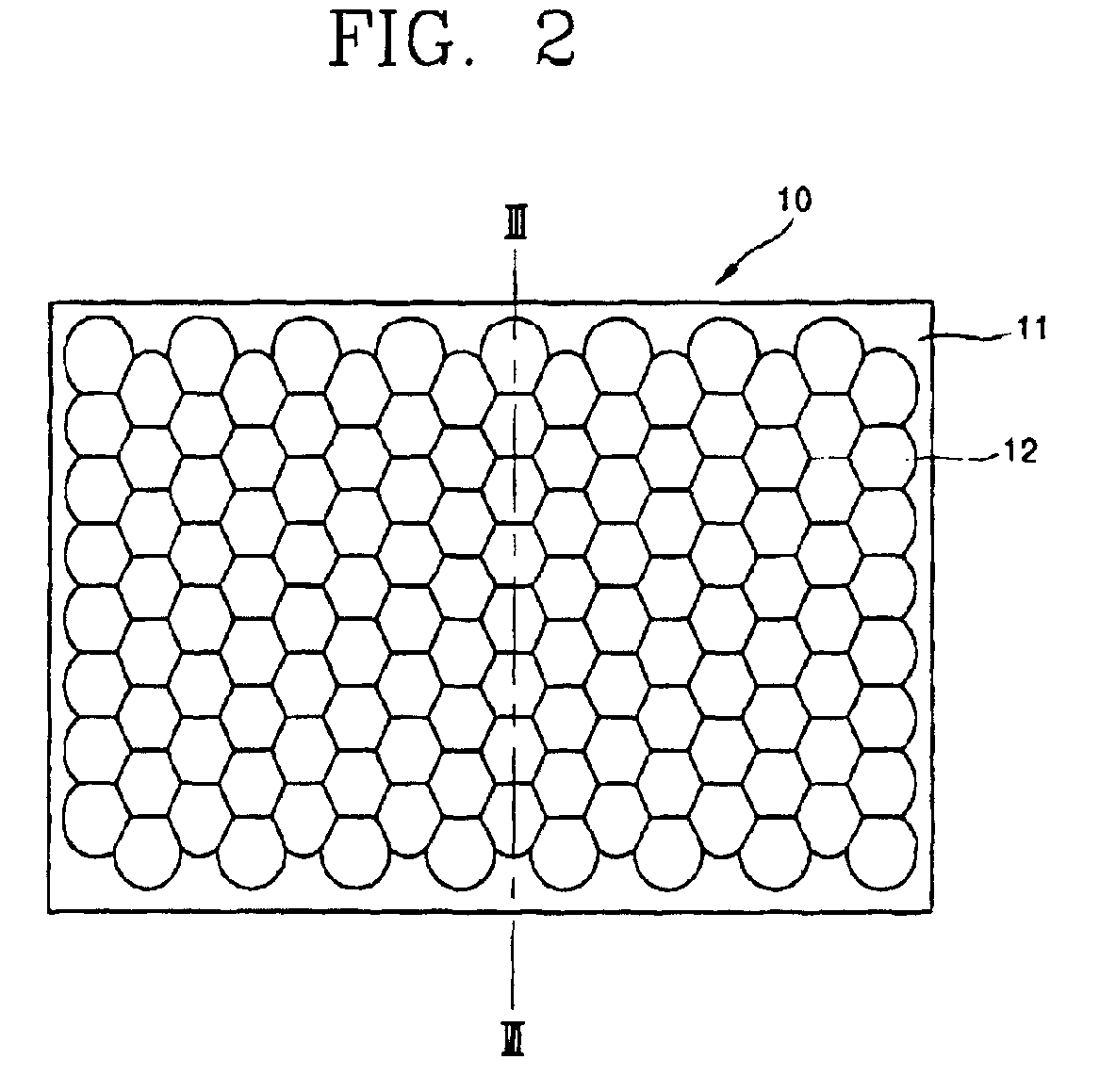
- Figure 2 is a plane view of the microstructure mold shown in Figure 1
- Figure 3 is a cross-sectional view according to a cut-line III-III shown in Figure 2
- Figure 4 is an enlarged view showing a main part A shown in Figure 3
- Figure 5 is an enlarged view showing a main part B shown in Figure 4.
- the microstructure mold 10 in accordance with an embodiment of the present invention includes: a mold substrate 11 having a microstructure pattern 12 to be transferred to a molding 20 on one surface thereof; and a monolayer coated on the mold substrate 11 in order to facilitate the mold to be released from the molding 20.
- the mold 10 is generally manufactured by using an MEMS (Micro Electro Mechanical System) technique which includes electroplating or electroless plating on a master in which a certain microstructure pattern is defined.
- MEMS Micro Electro Mechanical System
- the microstructure pattern 12 formed at the mold 10 may be manufactured by a mechanical working.
- the embodiment shows the microstructure mold for manufacturing a micro-lens array having an outer diameter at a range of a micron to one millimeter.
- a surfactant bonding to the surface of the mold 10 is used as a release agent forming the monolayer 13. That is, the surfactant containing a precursor having a particular functional group and a hydrophobic chain structure forms the monolayer 13.
- the surfactant is bonded well to the mold 10 surface by a chemical adsorption and well aligned by itself. That is, the surfactant forms a monolayer called Self Assembled Monolayer (SAM) by a self assembly method on the surface of the mold 10.
- SAM Self Assembled Monolayer
- the surfactant is bonded to the mold surface by a van der Waals' force and a covalent bonding so that it can be strongly bonded to the surface of the mold 10.
- the surfactant forming the monolayer 13 is appropriately selected according to a material of the mold 10.
- a thiol-based precursor is preferably used as the surfactant.
- one of precursors namely, a sulfides, disulfides, RSO 2 H and R 3 P is preferably selected and used as the surfactant.
- a method for coating a microstructure mold in accordance with an embodiment of the present invention includes: a first step of wetting a surface of the microstructure mold 10 with a mixed solution of a surfactant and an organic solvent; a second step of the surfactant's reacting upon the surface of the mold 10 and then coating a monolayer 13 formed of the surfactant on the surface of the mold 10; a third step of removing the surfactant without having reacted upon the surface of the mold 10 therefrom; and a fourth step of drying the microstructure mold 10 on which the monolayer 13 has been formed.
- a molar concentration of the mixed solution should be decided within a proper range in order to obtain a superior coating monolayer 13, namely, preferably within the range of 1 mM to 10mM.
- N and N-dimethylformamide (DMF) are usually used as the organic solvent mixed with the surfactant.
- a dipping method can be explained therefor. That is, by dipping the mold in the mixed solution for a certain time, the surfactants in the mixed solution are bonded to the surface of the mold 10 by a van der Waals' force and a covalent bonding thereby to form the monolayer 13.
- the surface of the mold 10 is reacted upon the surfactant in the mixed solution flowing in the passage thereby to form the monolayer 13. According to this, a characteristic of thin film of the monolayer 13 can be improved and a processing time can be shortened.
- the mold 10 can be surely reacted upon the surfactant by using other methods.
- Such formed monolayer 13 is the SAM formed by the self assembly method as stated above.
- the surfactant can be bonded to the surface of the mold 10 better.
- the monolayer 13 is formed on the surface of the mold 10 but the mixed solution containing a surfactant which hasn't been bonded to the surface of the mold 10 still remains on the surface of the mold 10. Therefore, it is necessary to remove the residual mixed solution from the surface of the mold 13.
- the surface of the mold having the monolayer 13 thereon is washed with the organic solvent such as acetone, isoprophyl alcohol or the like and thus the mixed solution containing the surfactant remaining on the mold surface is removed.
- the mold 10 is dried under 100°C for a certain time through a thermal stabilization process and the residual organic solvent on the surface of the mold 13 is completely evaporated and also the monolayer 13 is coated on the surface of the mold 10 more strongly.
- the self assembled monolayer 13 is about several nanometers (nm) thick. Accordingly, the monolayer 13 has a proper releasing performance without impeding a precision of the microstructure pattern 12 formed on the mold 10, thereby easily releasing the molding 20 from the mold 10.
- a thiol-based precursor is preferably selected as the surfactant.
- one of precursors namely, a sulfides, disulfides, RSO 2 H and R 3 P is preferably selected and used as the surfactant.
- the microstructure mold and the method for coating the same are provided, by which the microstructure mold can have a proper releasing performance without impeding precision of the mold by coating a coating material formed of the surfactant on the mold surface with a monolayer which is several namometers (nm) thick
- the coating layer formed on the microstructure mold of the present invention is obtained by a wetting method such as dipping it in the mixed solution containing the surfactant using a principle for forming the self assembled monolayer (SAM).
- SAM self assembled monolayer
- the coating layer can maintain its uniform thickness without using a complex equipment like a plasma evaporation. According to this, processing costs can be remarkably reduced such by minimizing capital investment costs required for coating and a mass production using semiconductor integrated process is possible.
- the coating layer of the microstructure mold of the present invention is formed on the mold surface by a covalent bonding and a van der Waals' force so that it is bonded to the mold surface with relatively high bond energy in comparison to the existing coating method. Therefore, reliability of the mold and the molding formed thereby can be improved and corrosion resistance of the mold surface can be improved as well.
- microstructure mold and the method for coating the same in accordance with the present invention can be utilized for a microstructure mold including such a micro-lens array seat manufactured by a micromachining and an MEMS (Micro Electromechanical System) technique.
- MEMS Micro Electromechanical System
Landscapes
- Engineering & Computer Science (AREA)
- Chemical & Material Sciences (AREA)
- Mechanical Engineering (AREA)
- Physics & Mathematics (AREA)
- Manufacturing & Machinery (AREA)
- Nanotechnology (AREA)
- General Physics & Mathematics (AREA)
- Materials Engineering (AREA)
- Crystallography & Structural Chemistry (AREA)
- Condensed Matter Physics & Semiconductors (AREA)
- Composite Materials (AREA)
- Optics & Photonics (AREA)
- General Chemical & Material Sciences (AREA)
- Chemical Kinetics & Catalysis (AREA)
- Metallurgy (AREA)
- Organic Chemistry (AREA)
- Microelectronics & Electronic Packaging (AREA)
- Moulds For Moulding Plastics Or The Like (AREA)
- Application Of Or Painting With Fluid Materials (AREA)
Abstract
Description
Claims (23)
- A microstructure mold having a monolayer coated on a surface thereof for release from a molding.
- The microstructure mold of claim 1, wherein the monolayer is formed by bonding a surfactant on the mold surface
- The microstructure mold of claim 2, wherein the monolayer is formed by a self assembly method.
- The microstructure mold of claim 2, wherein a material of the mold is one of cuprum (Cu), nickel (Ni), palladium (Pd), aurum (Au) and argentum (Ag).
- The microstructure mold of claim 4, wherein the surfactant is a thiol-based precursor.
- The microstructure mold of claim 2, wherein the material of the mold is aurum (Au).
- The microstructure mold of claim 6, wherein the surfactant is one of precursors, namely, sulfides, disulfides, RSO2H and R3P.
- The microstructure mold of claim 2, wherein the surfactant is bonded on the mold surface according to a van der Waals' force and a covalent bonding.
- The microstructure mold of claim 1, wherein the microstructure mold is a mold for molding a micro-lens array seat.
- A method for coating a microstructure mold comprising:a first step of wetting a microstructure mold surface with a solution obtained by mixing a surfactant and an organic solvent;a second step of the surfactant's reacting upon the mold surface thereby coating the monolayer formed of the surfactant on the mold surface;a third step of removing the surfactant, which has not reacted upon the mold surface, from the mold surface; anda fourth step of drying the microstructure mold on which the monolayer is formed.
- The method of claim 10, wherein a molar concentration of the mixed solution is 1 mM to 10mM.
- The method of claim 10, wherein the first step is achieved by dipping the mold in the mixed solution for a certain time.
- The method of claim 10, wherein the first step is achieved by flowing the mixed solution into a passage formed in the mold.
- The method of claim 10, wherein further comprising a step of washing the mold with an organic solvent prior to the first step.
- The method of claim 10, wherein the organic solvent is N and N-dimethylformamide (DMF).
- The method of claim 10, wherein the monolayer is formed by a self assembly method.
- The method of claim 10, wherein in the third step, the mold surface where the monolayer is formed is washed with the organic solvent thereby to remove a mixed solution containing the surfactant remaining on the mold surface.
- The method of claim 10, wherein in the fourth step, the mold is dried through a thermal stabilization process under 100°C for a certain time.
- The method of claim 10, wherein the material of the mold is one of cuprum (Cu), nickel (Ni), palladium (Pd), aurum (Au), and argentum (Ag).
- The microstructure mold of claim 19, wherein the surfactant is a thiol-based precursor.
- The microstructure mold of claim 10, wherein the material of the mold is aurum (Au).
- The microstructure mold of claim 21, wherein the surfactant is one of precursors, namely, sulfides, disulfides, RSO2H and R3P.
- The method of claim 10, wherein the monolayer is formed by bonding the surfactant on the mold surface depending on a van der Waals' force and a covalent bonding.
Applications Claiming Priority (2)
| Application Number | Priority Date | Filing Date | Title |
|---|---|---|---|
| KR1020030102239A KR100595515B1 (en) | 2003-12-31 | 2003-12-31 | Single layer film release agent coating method of mold for forming microstructure and mold for forming microstructure |
| KR2003102239 | 2003-12-31 |
Publications (2)
| Publication Number | Publication Date |
|---|---|
| EP1550540A2 true EP1550540A2 (en) | 2005-07-06 |
| EP1550540A3 EP1550540A3 (en) | 2005-11-09 |
Family
ID=34567874
Family Applications (1)
| Application Number | Title | Priority Date | Filing Date |
|---|---|---|---|
| EP04293149A Withdrawn EP1550540A3 (en) | 2003-12-31 | 2004-12-28 | Microstructure mold and method for coating the same |
Country Status (5)
| Country | Link |
|---|---|
| US (1) | US20050142286A1 (en) |
| EP (1) | EP1550540A3 (en) |
| JP (1) | JP2005193668A (en) |
| KR (1) | KR100595515B1 (en) |
| CN (1) | CN1636694A (en) |
Families Citing this family (6)
| Publication number | Priority date | Publication date | Assignee | Title |
|---|---|---|---|---|
| US8142703B2 (en) * | 2005-10-05 | 2012-03-27 | Molecular Imprints, Inc. | Imprint lithography method |
| US20090041986A1 (en) * | 2007-06-21 | 2009-02-12 | 3M Innovative Properties Company | Method of making hierarchical articles |
| US20090114618A1 (en) * | 2007-06-21 | 2009-05-07 | 3M Innovative Properties Company | Method of making hierarchical articles |
| US20080315459A1 (en) * | 2007-06-21 | 2008-12-25 | 3M Innovative Properties Company | Articles and methods for replication of microstructures and nanofeatures |
| CN102791453B (en) * | 2010-03-08 | 2014-08-06 | 夏普株式会社 | Mold release treatment method, mold, method for producing anti-reflective film, mold release treatment device, and washing/drying device for mold |
| KR101237336B1 (en) | 2011-05-20 | 2013-02-28 | 남구현 | Mold for making resin palte having surface effect of unglazed pottery appearance, methods of manufacturing of plate for use in such mold and resin plate produced thereby |
Family Cites Families (10)
| Publication number | Priority date | Publication date | Assignee | Title |
|---|---|---|---|---|
| NL8301482A (en) * | 1983-04-27 | 1984-11-16 | Philips Nv | DIE AND METHOD FOR THE MANUFACTURE OF PLASTIC ARTICLES USING THE DIE. |
| NL8401922A (en) * | 1984-06-18 | 1986-01-16 | Philips Nv | DIE AND METHOD FOR MANUFACTURING POLYURETHANE PRODUCTS AND LIGHTING LUMINAIRE MANUFACTURED BY THE METHOD. |
| JPH0818336B2 (en) * | 1991-02-06 | 1996-02-28 | 松下電器産業株式会社 | Molding member and manufacturing method thereof |
| JP2001030306A (en) * | 1999-07-27 | 2001-02-06 | Nippon Sheet Glass Co Ltd | Resin erect lens array and its manufacture |
| ATE332517T1 (en) * | 2000-01-21 | 2006-07-15 | Obducat Ab | MOLD FOR NANOPRINTING |
| JP2002026921A (en) * | 2000-07-05 | 2002-01-25 | Ricoh Co Ltd | Remote management system |
| CN100365507C (en) * | 2000-10-12 | 2008-01-30 | 德克萨斯州大学系统董事会 | Templates for low-pressure micro- and nano-scoring lithography at room temperature |
| GB2371248A (en) * | 2000-12-04 | 2002-07-24 | Seiko Epson Corp | Fabrication of self-assembled monolayers |
| JP2002196106A (en) * | 2000-12-27 | 2002-07-10 | Seiko Epson Corp | Microlens array, method of manufacturing the same, and optical device |
| US6656398B2 (en) * | 2001-06-19 | 2003-12-02 | Corning Incorporated | Process of making a pattern in a film |
-
2003
- 2003-12-31 KR KR1020030102239A patent/KR100595515B1/en not_active Expired - Fee Related
-
2004
- 2004-12-27 JP JP2004377583A patent/JP2005193668A/en active Pending
- 2004-12-28 EP EP04293149A patent/EP1550540A3/en not_active Withdrawn
- 2004-12-29 US US11/023,552 patent/US20050142286A1/en not_active Abandoned
- 2004-12-31 CN CNA2004101031535A patent/CN1636694A/en active Pending
Also Published As
| Publication number | Publication date |
|---|---|
| KR20050071230A (en) | 2005-07-07 |
| CN1636694A (en) | 2005-07-13 |
| KR100595515B1 (en) | 2006-07-03 |
| JP2005193668A (en) | 2005-07-21 |
| EP1550540A3 (en) | 2005-11-09 |
| US20050142286A1 (en) | 2005-06-30 |
Similar Documents
| Publication | Publication Date | Title |
|---|---|---|
| KR20090117699A (en) | Imprint mold and its manufacturing method | |
| JP4466074B2 (en) | Fine metal structure and manufacturing method thereof, and fine mold and device | |
| US20090074955A1 (en) | Methods for patterning electronic elements and fabricating molds | |
| JP2001284798A5 (en) | ||
| EP1550540A2 (en) | Microstructure mold and method for coating the same | |
| EP2263972A1 (en) | Method for manufacturing a metal microstructure and microstructure obtained according to this method | |
| KR20080102989A (en) | Cleaning method of metal mask | |
| US20120282442A1 (en) | Mold Manufacture Method and Mold Formed by Said Method | |
| CN101995766A (en) | Metal microstructure forming method | |
| US7288327B2 (en) | Plated structures or components | |
| JP4550569B2 (en) | Electroforming mold and manufacturing method thereof | |
| JP2007022064A (en) | Method for producing mold for producing polymer base material having hydrophobic surface | |
| KR20150126705A (en) | Manufacturing method for metal component, and casting mold and mold release film used for same | |
| JP2006168297A (en) | Printing plate and printing plate manufacturing method | |
| KR101715177B1 (en) | Method for Fabricating Nickel Stamps with Micropattern | |
| JP4872052B2 (en) | Fine mold core material | |
| US7858003B2 (en) | Soft mold having back-plane attached thereto and method for fabricating the soft mold | |
| US20120107195A1 (en) | Method of producing microfluidic devices based on a polymer | |
| KR20210079212A (en) | Method for manufacturing a horological component and component produced according to said method | |
| CN119898728A (en) | A method for preparing a high-precision large-area ultra-thin hollow hard mask | |
| KR101937370B1 (en) | Transparent Conducting Dry Adhesive Film and method for manufacturing the same | |
| KR100926977B1 (en) | Imprint mold with release film and release film formation method of imprint mold | |
| CN112198759B (en) | Imprint mold, method for producing imprint mold, and nanoimprint method | |
| KR100991693B1 (en) | Mother mold for duplication of mold by electroplating and manufacturing method thereof | |
| JP2003127144A (en) | Aluminum mold for molding urethane resin and method for producing urethane resin |
Legal Events
| Date | Code | Title | Description |
|---|---|---|---|
| PUAI | Public reference made under article 153(3) epc to a published international application that has entered the european phase |
Free format text: ORIGINAL CODE: 0009012 |
|
| 17P | Request for examination filed |
Effective date: 20050103 |
|
| AK | Designated contracting states |
Kind code of ref document: A2 Designated state(s): AT BE BG CH CY CZ DE DK EE ES FI FR GB GR HU IE IS IT LI LT LU MC NL PL PT RO SE SI SK TR |
|
| AX | Request for extension of the european patent |
Extension state: AL BA HR LV MK YU |
|
| RIN1 | Information on inventor provided before grant (corrected) |
Inventor name: SEONG, DONG-MUG Inventor name: PARK, KI-WON Inventor name: LEE, GUN-WOO Inventor name: KWON, HYOUK Inventor name: OH, CHANG-HOON Inventor name: YEE, YOUNG-JOOTAPMAEUL GYEONGNAM APT. 707-304 |
|
| RAP1 | Party data changed (applicant data changed or rights of an application transferred) |
Owner name: LG MICRON LTD. Owner name: LG ELECTRONICS INC. |
|
| PUAL | Search report despatched |
Free format text: ORIGINAL CODE: 0009013 |
|
| AK | Designated contracting states |
Kind code of ref document: A3 Designated state(s): AT BE BG CH CY CZ DE DK EE ES FI FR GB GR HU IE IS IT LI LT LU MC NL PL PT RO SE SI SK TR |
|
| AX | Request for extension of the european patent |
Extension state: AL BA HR LV MK YU |
|
| AKX | Designation fees paid |
Designated state(s): DE FR GB NL |
|
| 17Q | First examination report despatched |
Effective date: 20060213 |
|
| STAA | Information on the status of an ep patent application or granted ep patent |
Free format text: STATUS: THE APPLICATION IS DEEMED TO BE WITHDRAWN |
|
| 18D | Application deemed to be withdrawn |
Effective date: 20080722 |