EP1548887A1 - Connector with integrated board - Google Patents
Connector with integrated board Download PDFInfo
- Publication number
- EP1548887A1 EP1548887A1 EP04106063A EP04106063A EP1548887A1 EP 1548887 A1 EP1548887 A1 EP 1548887A1 EP 04106063 A EP04106063 A EP 04106063A EP 04106063 A EP04106063 A EP 04106063A EP 1548887 A1 EP1548887 A1 EP 1548887A1
- Authority
- EP
- European Patent Office
- Prior art keywords
- board
- connection terminals
- connector
- connector housing
- joint connector
- Prior art date
- Legal status (The legal status is an assumption and is not a legal conclusion. Google has not performed a legal analysis and makes no representation as to the accuracy of the status listed.)
- Withdrawn
Links
- 239000010410 layer Substances 0.000 claims description 26
- 239000002356 single layer Substances 0.000 claims description 12
- 230000013011 mating Effects 0.000 claims description 9
- 238000010276 construction Methods 0.000 description 6
- 238000000034 method Methods 0.000 description 3
- 238000003780 insertion Methods 0.000 description 2
- 230000037431 insertion Effects 0.000 description 2
- 238000010030 laminating Methods 0.000 description 2
- 230000002265 prevention Effects 0.000 description 2
- 230000000717 retained effect Effects 0.000 description 2
- 239000000853 adhesive Substances 0.000 description 1
- 230000001070 adhesive effect Effects 0.000 description 1
- 239000007769 metal material Substances 0.000 description 1
- 238000000465 moulding Methods 0.000 description 1
- 229920003002 synthetic resin Polymers 0.000 description 1
- 239000000057 synthetic resin Substances 0.000 description 1
Images




Classifications
-
- H—ELECTRICITY
- H01—ELECTRIC ELEMENTS
- H01R—ELECTRICALLY-CONDUCTIVE CONNECTIONS; STRUCTURAL ASSOCIATIONS OF A PLURALITY OF MUTUALLY-INSULATED ELECTRICAL CONNECTING ELEMENTS; COUPLING DEVICES; CURRENT COLLECTORS
- H01R12/00—Structural associations of a plurality of mutually-insulated electrical connecting elements, specially adapted for printed circuits, e.g. printed circuit boards [PCB], flat or ribbon cables, or like generally planar structures, e.g. terminal strips, terminal blocks; Coupling devices specially adapted for printed circuits, flat or ribbon cables, or like generally planar structures; Terminals specially adapted for contact with, or insertion into, printed circuits, flat or ribbon cables, or like generally planar structures
- H01R12/50—Fixed connections
- H01R12/51—Fixed connections for rigid printed circuits or like structures
- H01R12/52—Fixed connections for rigid printed circuits or like structures connecting to other rigid printed circuits or like structures
- H01R12/523—Fixed connections for rigid printed circuits or like structures connecting to other rigid printed circuits or like structures by an interconnection through aligned holes in the boards or multilayer board
-
- H—ELECTRICITY
- H01—ELECTRIC ELEMENTS
- H01R—ELECTRICALLY-CONDUCTIVE CONNECTIONS; STRUCTURAL ASSOCIATIONS OF A PLURALITY OF MUTUALLY-INSULATED ELECTRICAL CONNECTING ELEMENTS; COUPLING DEVICES; CURRENT COLLECTORS
- H01R13/00—Details of coupling devices of the kinds covered by groups H01R12/70 or H01R24/00 - H01R33/00
- H01R13/66—Structural association with built-in electrical component
- H01R13/665—Structural association with built-in electrical component with built-in electronic circuit
- H01R13/6658—Structural association with built-in electrical component with built-in electronic circuit on printed circuit board
-
- H—ELECTRICITY
- H01—ELECTRIC ELEMENTS
- H01R—ELECTRICALLY-CONDUCTIVE CONNECTIONS; STRUCTURAL ASSOCIATIONS OF A PLURALITY OF MUTUALLY-INSULATED ELECTRICAL CONNECTING ELEMENTS; COUPLING DEVICES; CURRENT COLLECTORS
- H01R31/00—Coupling parts supported only by co-operation with counterpart
- H01R31/08—Short-circuiting members for bridging contacts in a counterpart
-
- H—ELECTRICITY
- H01—ELECTRIC ELEMENTS
- H01R—ELECTRICALLY-CONDUCTIVE CONNECTIONS; STRUCTURAL ASSOCIATIONS OF A PLURALITY OF MUTUALLY-INSULATED ELECTRICAL CONNECTING ELEMENTS; COUPLING DEVICES; CURRENT COLLECTORS
- H01R9/00—Structural associations of a plurality of mutually-insulated electrical connecting elements, e.g. terminal strips or terminal blocks; Terminals or binding posts mounted upon a base or in a case; Bases therefor
- H01R9/22—Bases, e.g. strip, block, panel
- H01R9/24—Terminal blocks
- H01R9/2458—Electrical interconnections between terminal blocks
- H01R9/2466—Electrical interconnections between terminal blocks using a planar conductive structure, e.g. printed circuit board
Definitions
- This invention relates to a joint connector for connecting a plurality of connection terminals together which are provided, for example, within a mating connector housing.
- a joint connector of this kind is used for obtaining a plurality of branch wire portions from a trunk wire portion of a wire harness employed, for example, in an electric system of an automobile or the like, and generally, a technique as disclosed for example in JP-A-8-17531 is known.
- a joint connector 1 of JP-A-8-17531 includes a connector housing 2, a pair of connection terminals 3 for being fixed to the connector housing 2, and an inter-terminal connecting portion 4 electrically connecting the connection terminals 3 together.
- the inter-terminal connecting portion 4 is formed by a bus bar, and is adapted to be inserted in a rear side of the connector housing 2.
- This invention has been made in view of the above circumstances, and an object of the invention is to provide a joint connector which can be formed into a compact, lightweight and low-cost design, and can be enhanced in the degree of freedom of a circuitry design, and can be easily assembled.
- a joint connector comprising:
- the board is a multi-layer board having a plurality of board portions which are laminated to each other.
- a plurality of the conductive wires are respectively formed on the board portions.
- the connection terminals contact to the conductive wire formed on a predetermined board portion of the board portions.
- the board is a single-layer board having a front face and rear face.
- a plurality of the conductive wires are respectively formed on the front and rear faces of the single-layer board.
- the connection terminals contact to the conductive wire formed on at least one of the front and rear faces of the single-layer board.
- a circuit which is connected to the conductive wire, is formed on the board.
- the connector housing has a mating terminal portion for mating with another terminal to be electrically connected to the connection terminals.
- the plurality of connection terminals are fixed to the connector housing, and press-fit portions of the plurality of connection terminals are inserted in the multi-layer board or the single-layer board.
- the joint connector of the invention is formed.
- either the multi-layer board or the single-layer board is used, and the multi-layer board is formed by laminating the board portions (each having the circuit formed thereon by printing), that is, the printed circuit boards, together.
- the single-layer board includes a single double-sided printed circuit board having the circuits formed on the front and rear sides thereof by printing.
- connection terminal when inserted into the multi-layer board or the single-layer board, is resiliently deformed to be kept in a press-fitted condition.
- press-fit portions contact the board, and are electrically connected to the corresponding circuits, the desired connection terminals are electrically connected together. This connection is effected collectively.
- the joint connector further comprises a cover, fitted to the connector housing to cover the board.
- the cover when the cover is fitted to the connector housing, the multi-layer board or the single-layer board in which the plurality of connection terminals are inserted is protected by the cover. And besides, the multi-layer board or the single-layer board is held by the cover, and is prevented from dropping.
- the joint connector employs the connection terminals each having the press-fit portion, the board (i.e., the printed circuit board) having the circuits formed thereon by printing, and the plurality of connection terminals, fixed to the connector housing, are electrically connected to the corresponding circuits of the printed circuit board, so that the desired connection terminals are collectively electrically connected together. Therefore, there are achieved advantages that this joint connector can be formed into a more compact, lightweight and lower-cost design as compared with the related structure employing bus bars, and that the degree of freedom of the circuitry design can be enhanced, and the assembling operation can be effected easily.
- the cover is fitted to the connector housing, and therefore there are achieved advantages that the multi-layer board or the single board is protected by the cover, and also is held by the cover against dropping and that the assembling operation can be effected easily.
- Fig. 1 is an exploded, perspective view of one preferred embodiment of a joint connector of the present invention.
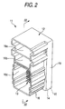
- Fig. 2 is a perspective view of the joint connector
- Fig. 3 is a cross-sectional view taken along the line III-III of Fig. 2
- Fig. 4 is an enlarged cross-sectional view of an important portion of Fig. 3
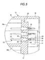
- Fig. 5 is an enlarged cross-sectional view of an important portion, showing a condition in which connection terminals are fixed to a connector housing.
- connection terminal 11 denotes the joint connector of the invention.
- This joint connector 11 includes the connector housing 12, a plurality of connection terminals 13 for being fixed to the connector housing 12, a multi-layer board 14 in which the connection terminals 13 can be inserted, and a cover 15 for fitting to a rear side of the connector housing 12. The constructions of these parts will be described below in detail
- the connector housing 12 is molded of an insulative synthetic resin, and a fitting portion 16 into which connector housings of a plurality of mating connectors (not shown) can be fitted is formed in a front side of the connector housing 12.
- a terminal fixing portion 17 for the plurality of connection terminals 13 is formed within the connector housing 12, and is disposed intermediate the front and rear sides thereof.
- a board receiving portion 18 is formed at the rear side of the connector housing 12, and the multi-layer board 14 is received in the board receiving portion 18, and the cover 15 is fitted in this board receiving portion 18.
- the fitting portion 16 is so shaped as to guide the connector housings of the mating connectors during the insertion of these connector housings and also to retain the inserted connector housings.
- the fitting portion 16 though not limited to such a construction, has three fitting portions (first to third fitting portions 16a to 16c).
- the terminal fixing portion 17 is defined by an inner end wall disposed at the inner end of the fitting portion 16, and a plurality of through holes 19 for terminal press-fitting purposes are formed through the terminal fixing portion 17.
- the through holes 19 are formed through the terminal fixing portion 17, and extend perpendicularly to the front and rear sides of this terminal fixing portion 17.
- Each through hole 19 is formed into such a stepped shape that the connection terminal 13, when inserted into the through hole 19 from that side (i.e., the front side) of the terminal fixing portion 17 facing the terminal fixing portion 16, can be stopped at a predetermined position.
- the number of the through holes 19 is as follows (This number is given merely as one example).
- 3 x 9 through holes 19 are formed through each of those portions of the terminal fixing portion 17 corresponding respectively to the first and second fixing portions 16a and 16b, while 11 ⁇ 9 through holes 19 are formed through that portion of the terminal fixing portion 17 corresponding to the third fitting portion 16c.
- connection terminals 13 are adapted to be press-fitted in the respective through holes 19 in the terminal fixing portion 17, and are fixed thereto, this embodiment is not limited to this construction, and the connection terminals can be fixed to the terminal fixing portion by insert molding.
- the board receiving portion 18 is formed to be open to the rear side of the connector housing 12.
- the depth and size of the board receiving portion 18 are determined in view of the thicknesses of the multi-layer board 14 and cover 15.
- a recess 20 for the insertion of a front end portion of the cover 15 thereinto is formed in the board receiving portion 18, and also retaining portions 21 with which retaining projections 35 (described later) of the cover 15 can be retainingly engaged, respectively, are formed at the board receiving portion 18.
- connection terminals 13 are formed of an electrically-conductive metallic material.
- the connection terminal 13 includes a connector-contacting portion 22, a fixing portion 23, and a press-fit portion 24.
- the connection terminal 13 is formed, for example, into a generally pin-like shape.
- the connection terminal 13 may be called a press-fit terminal since it has the press-fit portion 24.
- the connector-contacting portion 22 projects into the fitting portion 16, and contacts a connection terminal of the mating connector.
- the connector-contacting portion 22 is formed into a pin-like shape, it is not limited to this shape, but can be formed into a tab-like shape.
- the fixing portion 23 is formed at a middle portion of the connection terminal 13. When the connection terminal 13 is fixed to the connector housing 12, the fixing portion 23 is press-fitted in the through hole 19 in the terminal fixing portion 17.
- the fixing portion 23 includes an abutment portion 25 for abutting against the stepped portion of the through hole 19, and a withdrawal prevention portion 26 for biting into the inner surface of the through hole 19.
- the abutment portion 25 is disposed close to the connector-contacting portion 22, while the withdrawal prevention portion 26 is disposed close to the press-fit portion 24.
- the press-fit portion 24 projects into the board receiving portion 18 to be inserted into the multi-layer board 14.
- the press-fit portion 24 includes a resiliently-deformable body portion 27 (having, for example, a generally oval shape) disposed close to the fixing portion 23, and a pin-like guide portion 28 which extends continuously from the body portion 27, and is disposed at the distal end portion.
- the multi-layer board 14 is a member comprising a plurality of boards 29 laminated together, and this multi-layer board is formed, for example, by four boards 29a to 29d although the number of the boards is not particularly limited to four.
- the boards 29 are fixed to one another by suitable fixing portion such as an adhesive or a fixing member.
- a plurality of circuits 30, having respective predetermined path patterns, are formed by printing on each board 29.
- the circuits 30 correspond to inter-terminal connecting portions, and in this embodiment the plurality of circuits 30 are formed by printing on that surface (front surface) of the board from which the connection terminals 13 are inserted into the board.
- Each board 29 is similar in construction to a known printed circuit board.
- a plurality of through holes 31 are formed through each board 29 of the multi-layer board 14.
- the press-fit portions 24 of the connection terminals 13 are inserted into the through holes 31, and the number and arrangement of the through holes 31, formed in each board, correspond to the number and arrangement of the connection terminals 31, respectively.
- Each through hole 31 is formed into such a size that the body portion 27 of the press-fit portion 24, inserted into the through hole 31, can be resiliently deformed.
- the through holes 31 are classified into through holes 31 a, each having a circuit conducting portion (not shown) for electrically connecting the body portion 27 and the circuit 30 together, and through holes 31 b each in the form of a mere through hole not provided with the circuit conducting portion (not shown). By suitably using these through holes, desired connection terminals 13 can be electrically connected together.
- Each of the through holes 31 a has the circuit conducting portion (not shown), and therefore is formed through that portion of the board 29 at which the corresponding circuit 30 is formed.
- the through holes 31 b do not have the circuit conducting portion (not shown), and therefore are formed through those portions of the board 29 at which any circuit 30 is not formed.
- the single board is one printed circuit board, and is larger in thickness than the board 29, and circuits, having respective predetermined path patterns, are formed by printing on front and rear surfaces thereof.
- the single board is effectively used when it is smaller in the number of circuits than the multi-layer board 14.
- the cover 15 is a member which is inserted into the board receiving portion 18 of the connector housing 12, and is retained there.
- This cover 15 includes a bottom portion 32, and a side portion 33, and is formed into a box-like shape with a shallow bottom.
- the bottom portion 32 of the cover 15 is in the form of a flat plate, and a plurality of recesses 34 are formed in that side (or surface) of the bottom portion 32 facing the multi-layer board 14, and the press-fit portions 24 of the connection terminals 13, projecting through the multi-layer board 14, are inserted into the recesses 34, respectively.
- the recesses 34, formed in the bottom portion correspond in the number and arrangement to the connection terminals 13.
- the plurality of retaining projections 35 for retaining engagement respectively with the retaining portions 21 on the connector housing 12 are formed at the side portion 33 of the cover 15.
- the retaining projection 35 is formed into a claw-like shape. Further, a tapering surface is formed on the retaining projection 35 so as to achieve the smooth engagement.
- the provision of the cover 15 is arbitrary. When the cover is provided as in this embodiment, the cover effectively protects and retains the multi-layer board 14.
- connection terminals 13 are inserted or press-fitted respectively into the through holes 19 in the terminal fixing portion 17 of the connector housing 12, and are fixed thereto, and the press-fit portions 24 of the connection terminals 13 are projected into the board receiving portion 18 of the connector housing 12, and the multi-layer board 14 is attached to the connector housing 12 in such a manner that the press-fit portions 24 are inserted respectively into the corresponding through holes 31.
- the cover 15 is fitted in the connector housing 12, and is retained thereto in such a manner that this cover 15 covers the multi-layer board 14 received in the board receiving portion 18, thereby forming the joint connector 11 of the invention.
- a plurality of branch wire portions are obtained, for example, from one trunk wire portion of a wire harness.
- the joint connector 11 of the invention employs the multi-layer board 14 (or the above single board) formed by laminating the plurality of boards (printed circuit boards) 29 together, and therefore this joint connector can be formed into a more compact design than the related joint connector, and also the degree of freedom of the circuitry design can be enhanced (that is, is higher as compared with the structure in which joint connections are made by installing bus bars or wires).
- this joint connector can be formed into a more lightweight and lower-cost design than the related joint connector, and also the management of the parts as a whole can be simplified.
- the joint connector 11 of the invention is of such a structure that desired connection terminals 13 can be collectively joint-connected simultaneously when the multi-layer board 14 (or the above single board) is attached to the connector housing, and therefore the assembling operation can be effected easily.
Landscapes
- Coupling Device And Connection With Printed Circuit (AREA)
- Multi-Conductor Connections (AREA)
- Connection Or Junction Boxes (AREA)
Abstract
Description
- This invention relates to a joint connector for connecting a plurality of connection terminals together which are provided, for example, within a mating connector housing.
- A joint connector of this kind is used for obtaining a plurality of branch wire portions from a trunk wire portion of a wire harness employed, for example, in an electric system of an automobile or the like, and generally, a technique as disclosed for example in JP-A-8-17531 is known. Namely, as shown in Fig. 6, a joint connector 1 of JP-A-8-17531 includes a
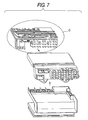
connector housing 2, a pair ofconnection terminals 3 for being fixed to theconnector housing 2, and an inter-terminal connectingportion 4 electrically connecting theconnection terminals 3 together. The inter-terminal connectingportion 4 is formed by a bus bar, and is adapted to be inserted in a rear side of theconnector housing 2. - In the joint connector using such a plug-in type bus bar as the inter-terminal connecting portion, when the number of connection terminals increases, the structure of a portion for effecting the connection between the terminals becomes complicated, and therefore there is used a joint technique (see, for example, JP-A-5-3619) employing bus bars and a board as commonly known in an electric connection box for mounting on an automobile. Namely, the structure as indicated by a circle C in Fig. 7 is used as the portion for effecting the connection between the terminals of the joint connector.
- When the number of connection terminals of the joint connector increases, the structure of the portion for effecting the connection between the terminals becomes complicated as described above, and therefore the kinds of bus bars to be used increase, and this invites problems that the management of the parts is complicated and that the weight, the cost and the time and labor for the operation increase. And besides, when the structure as indicated by circle C in Fig. 7 is used, the depth of the joint connector increases, thus inviting a problem that the overall size becomes large. Furthermore, when the structure as indicated by circle C in Fig. 7 is used, the degree of freedom of a circuitry design is limited, so that there is encountered a problem that such a structure can not meet a more complicated circuit arrangement.
- This invention has been made in view of the above circumstances, and an object of the invention is to provide a joint connector which can be formed into a compact, lightweight and low-cost design, and can be enhanced in the degree of freedom of a circuitry design, and can be easily assembled.
- In order to achieve the above object, according to the present invention, there is provided a joint connector, comprising:
- an insulative connector housing;
- a plurality of connection terminals, provided on the connector housing; and
- a board, on which a conductive wire is formed, wherein the connection terminals contact to the conductive wire for electrically connecting predetermined connection terminals of the connection terminals each other.
-
- Preferably, the board is a multi-layer board having a plurality of board portions which are laminated to each other. A plurality of the conductive wires are respectively formed on the board portions. The connection terminals contact to the conductive wire formed on a predetermined board portion of the board portions.
- Preferably, the board is a single-layer board having a front face and rear face. A plurality of the conductive wires are respectively formed on the front and rear faces of the single-layer board. The connection terminals contact to the conductive wire formed on at least one of the front and rear faces of the single-layer board.
- Preferably, a circuit, which is connected to the conductive wire, is formed on the board.
- Preferably, the connector housing has a mating terminal portion for mating with another terminal to be electrically connected to the connection terminals.
- In the above configurations, the plurality of connection terminals are fixed to the connector housing, and press-fit portions of the plurality of connection terminals are inserted in the multi-layer board or the single-layer board. As a result, the joint connector of the invention is formed. In the joint connector of the invention, either the multi-layer board or the single-layer board is used, and the multi-layer board is formed by laminating the board portions (each having the circuit formed thereon by printing), that is, the printed circuit boards, together. On the other hand, the single-layer board includes a single double-sided printed circuit board having the circuits formed on the front and rear sides thereof by printing. The press-fit portion of the connection terminal, when inserted into the multi-layer board or the single-layer board, is resiliently deformed to be kept in a press-fitted condition. When the press-fit portions contact the board, and are electrically connected to the corresponding circuits, the desired connection terminals are electrically connected together. This connection is effected collectively.
- Preferably, the joint connector further comprises a cover, fitted to the connector housing to cover the board.
- In the above configuration, when the cover is fitted to the connector housing, the multi-layer board or the single-layer board in which the plurality of connection terminals are inserted is protected by the cover. And besides, the multi-layer board or the single-layer board is held by the cover, and is prevented from dropping.
- In the above configurations, the joint connector employs the connection terminals each having the press-fit portion, the board (i.e., the printed circuit board) having the circuits formed thereon by printing, and the plurality of connection terminals, fixed to the connector housing, are electrically connected to the corresponding circuits of the printed circuit board, so that the desired connection terminals are collectively electrically connected together. Therefore, there are achieved advantages that this joint connector can be formed into a more compact, lightweight and lower-cost design as compared with the related structure employing bus bars, and that the degree of freedom of the circuitry design can be enhanced, and the assembling operation can be effected easily.
- Further, in the above configurations, the cover is fitted to the connector housing, and therefore there are achieved advantages that the multi-layer board or the single board is protected by the cover, and also is held by the cover against dropping and that the assembling operation can be effected easily.
- The above objects and advantages of the present invention will become more apparent by describing in detail preferred exemplary embodiments thereof with reference to the accompanying drawings, wherein:
- Fig. 1 is an exploded, perspective view of one preferred embodiment of a joint connector of the present invention;
- Fig. 2 is a perspective view of the joint connector of the invention;
- Fig. 3 is a cross-sectional view taken along the line III-III of Fig. 2;
- Fig. 4 is an enlarged cross-sectional view of an important portion of Fig. 3;
- Fig. 5 is an enlarged cross-sectional view of an important portion, showing a condition in which connection terminals are fixed to a connector housing;
- Fig. 6 is an exploded, perspective view of a related joint connector; and
- Fig. 7 is a view explanatory of a related joint technique employing bus bars and a board.
-
- The invention will now be described with reference to the drawings.
- Fig. 1 is an exploded, perspective view of one preferred embodiment of a joint connector of the present invention. Fig. 2 is a perspective view of the joint connector, Fig. 3 is a cross-sectional view taken along the line III-III of Fig. 2, Fig. 4 is an enlarged cross-sectional view of an important portion of Fig. 3, and Fig. 5 is an enlarged cross-sectional view of an important portion, showing a condition in which connection terminals are fixed to a connector housing.
- In Figs. 1 to 5,
reference numeral 11 denotes the joint connector of the invention. Thisjoint connector 11 includes theconnector housing 12, a plurality ofconnection terminals 13 for being fixed to theconnector housing 12, amulti-layer board 14 in which theconnection terminals 13 can be inserted, and acover 15 for fitting to a rear side of theconnector housing 12. The constructions of these parts will be described below in detail - The
connector housing 12 is molded of an insulative synthetic resin, and afitting portion 16 into which connector housings of a plurality of mating connectors (not shown) can be fitted is formed in a front side of theconnector housing 12. Aterminal fixing portion 17 for the plurality ofconnection terminals 13 is formed within theconnector housing 12, and is disposed intermediate the front and rear sides thereof. Aboard receiving portion 18 is formed at the rear side of theconnector housing 12, and themulti-layer board 14 is received in theboard receiving portion 18, and thecover 15 is fitted in thisboard receiving portion 18. - The
fitting portion 16 is so shaped as to guide the connector housings of the mating connectors during the insertion of these connector housings and also to retain the inserted connector housings. Thefitting portion 16, though not limited to such a construction, has three fitting portions (first to third fittingportions 16a to 16c). - The
terminal fixing portion 17 is defined by an inner end wall disposed at the inner end of thefitting portion 16, and a plurality of throughholes 19 for terminal press-fitting purposes are formed through theterminal fixing portion 17. The throughholes 19 are formed through theterminal fixing portion 17, and extend perpendicularly to the front and rear sides of thisterminal fixing portion 17. Each throughhole 19 is formed into such a stepped shape that theconnection terminal 13, when inserted into the throughhole 19 from that side (i.e., the front side) of theterminal fixing portion 17 facing theterminal fixing portion 16, can be stopped at a predetermined position. In this embodiment, the number of the throughholes 19 is as follows (This number is given merely as one example). Namely, 3 x 9 throughholes 19 are formed through each of those portions of theterminal fixing portion 17 corresponding respectively to the first andsecond fixing portions holes 19 are formed through that portion of theterminal fixing portion 17 corresponding to thethird fitting portion 16c. - In this embodiment, although the
connection terminals 13 are adapted to be press-fitted in the respective throughholes 19 in theterminal fixing portion 17, and are fixed thereto, this embodiment is not limited to this construction, and the connection terminals can be fixed to the terminal fixing portion by insert molding. - The
board receiving portion 18 is formed to be open to the rear side of theconnector housing 12. The depth and size of theboard receiving portion 18 are determined in view of the thicknesses of themulti-layer board 14 andcover 15. Arecess 20 for the insertion of a front end portion of thecover 15 thereinto is formed in theboard receiving portion 18, and also retainingportions 21 with which retaining projections 35 (described later) of thecover 15 can be retainingly engaged, respectively, are formed at theboard receiving portion 18. - Each of the
connection terminals 13 is formed of an electrically-conductive metallic material. Theconnection terminal 13 includes a connector-contactingportion 22, a fixingportion 23, and a press-fit portion 24. Theconnection terminal 13 is formed, for example, into a generally pin-like shape. Theconnection terminal 13 may be called a press-fit terminal since it has the press-fit portion 24. - When the
connection terminal 13 is fixed to theconnector housing 12, the connector-contactingportion 22 projects into thefitting portion 16, and contacts a connection terminal of the mating connector. In this embodiment, although the connector-contactingportion 22 is formed into a pin-like shape, it is not limited to this shape, but can be formed into a tab-like shape. - The fixing
portion 23 is formed at a middle portion of theconnection terminal 13. When theconnection terminal 13 is fixed to theconnector housing 12, the fixingportion 23 is press-fitted in the throughhole 19 in theterminal fixing portion 17. The fixingportion 23 includes anabutment portion 25 for abutting against the stepped portion of the throughhole 19, and awithdrawal prevention portion 26 for biting into the inner surface of the throughhole 19. Theabutment portion 25 is disposed close to the connector-contactingportion 22, while thewithdrawal prevention portion 26 is disposed close to the press-fit portion 24. - When the
connection terminal 13 is fixed to theconnector housing 12, the press-fit portion 24 projects into theboard receiving portion 18 to be inserted into themulti-layer board 14. The press-fit portion 24 includes a resiliently-deformable body portion 27 (having, for example, a generally oval shape) disposed close to the fixingportion 23, and a pin-like guide portion 28 which extends continuously from thebody portion 27, and is disposed at the distal end portion. - The
multi-layer board 14 is a member comprising a plurality ofboards 29 laminated together, and this multi-layer board is formed, for example, by fourboards 29a to 29d although the number of the boards is not particularly limited to four. Theboards 29 are fixed to one another by suitable fixing portion such as an adhesive or a fixing member. A plurality ofcircuits 30, having respective predetermined path patterns, are formed by printing on eachboard 29. Thecircuits 30 correspond to inter-terminal connecting portions, and in this embodiment the plurality ofcircuits 30 are formed by printing on that surface (front surface) of the board from which theconnection terminals 13 are inserted into the board. Eachboard 29 is similar in construction to a known printed circuit board. - A plurality of through
holes 31 are formed through eachboard 29 of themulti-layer board 14. The press-fit portions 24 of theconnection terminals 13 are inserted into the throughholes 31, and the number and arrangement of the throughholes 31, formed in each board, correspond to the number and arrangement of theconnection terminals 31, respectively. Each throughhole 31 is formed into such a size that thebody portion 27 of the press-fit portion 24, inserted into the throughhole 31, can be resiliently deformed. - The through holes 31 are classified into through
holes 31 a, each having a circuit conducting portion (not shown) for electrically connecting thebody portion 27 and thecircuit 30 together, and throughholes 31 b each in the form of a mere through hole not provided with the circuit conducting portion (not shown). By suitably using these through holes, desiredconnection terminals 13 can be electrically connected together. Each of the throughholes 31 a has the circuit conducting portion (not shown), and therefore is formed through that portion of theboard 29 at which thecorresponding circuit 30 is formed. On the other hand, the throughholes 31 b do not have the circuit conducting portion (not shown), and therefore are formed through those portions of theboard 29 at which anycircuit 30 is not formed. - Instead of using the
multi-layer board 14, there can be used a single board. Although not particularly shown in the drawings, the single board is one printed circuit board, and is larger in thickness than theboard 29, and circuits, having respective predetermined path patterns, are formed by printing on front and rear surfaces thereof. The single board is effectively used when it is smaller in the number of circuits than themulti-layer board 14. - The
cover 15 is a member which is inserted into theboard receiving portion 18 of theconnector housing 12, and is retained there. Thiscover 15 includes abottom portion 32, and aside portion 33, and is formed into a box-like shape with a shallow bottom. Thebottom portion 32 of thecover 15 is in the form of a flat plate, and a plurality ofrecesses 34 are formed in that side (or surface) of thebottom portion 32 facing themulti-layer board 14, and the press-fit portions 24 of theconnection terminals 13, projecting through themulti-layer board 14, are inserted into therecesses 34, respectively. Therecesses 34, formed in the bottom portion, correspond in the number and arrangement to theconnection terminals 13. - The plurality of retaining
projections 35 for retaining engagement respectively with the retainingportions 21 on theconnector housing 12 are formed at theside portion 33 of thecover 15. The retainingprojection 35 is formed into a claw-like shape. Further, a tapering surface is formed on the retainingprojection 35 so as to achieve the smooth engagement. - The provision of the
cover 15 is arbitrary. When the cover is provided as in this embodiment, the cover effectively protects and retains themulti-layer board 14. - In the above construction, the
connection terminals 13 are inserted or press-fitted respectively into the throughholes 19 in theterminal fixing portion 17 of theconnector housing 12, and are fixed thereto, and the press-fit portions 24 of theconnection terminals 13 are projected into theboard receiving portion 18 of theconnector housing 12, and themulti-layer board 14 is attached to theconnector housing 12 in such a manner that the press-fit portions 24 are inserted respectively into the corresponding through holes 31. Thereafter, thecover 15 is fitted in theconnector housing 12, and is retained thereto in such a manner that thiscover 15 covers themulti-layer board 14 received in theboard receiving portion 18, thereby forming thejoint connector 11 of the invention. - When the mating connectors are connected to the
fitting portion 16 of thejoint connector 11 of the invention, a plurality of branch wire portions are obtained, for example, from one trunk wire portion of a wire harness. - As described above with reference to Figs. 1 to 5, the
joint connector 11 of the invention employs the multi-layer board 14 (or the above single board) formed by laminating the plurality of boards (printed circuit boards) 29 together, and therefore this joint connector can be formed into a more compact design than the related joint connector, and also the degree of freedom of the circuitry design can be enhanced (that is, is higher as compared with the structure in which joint connections are made by installing bus bars or wires). - And besides, in the
joint connector 11 of the invention, bus bars as used in the related construction are not used, and instead the multi-layer board 14 (or the above single board) having thecircuits 30 formed thereon by printing, are used. Therefore, this joint connector can be formed into a more lightweight and lower-cost design than the related joint connector, and also the management of the parts as a whole can be simplified. - Furthermore, the
joint connector 11 of the invention is of such a structure that desiredconnection terminals 13 can be collectively joint-connected simultaneously when the multi-layer board 14 (or the above single board) is attached to the connector housing, and therefore the assembling operation can be effected easily. - And besides, the invention can be modified in various ways within the scope of the invention, that is, without departing from the subject matter of the invention.
Claims (6)
- A joint connector, comprising:wherein the connection terminals contact to the conductive wire for electrically connecting predetermined connection terminals of the connection terminals each other.an insulative connector housing;a plurality of connection terminals, provided on the connector housing; anda board, on which a conductive wire is formed,
- The joint connector as set forth in claim 1, wherein the board is a multi-layer board having a plurality of board portions which are laminated to each other;
wherein a plurality of the conductive wires are respectively formed on the board portions; and
wherein the connection terminals contact to the conductive wire formed on a predetermined board portion of the board portions. - The joint connector as set forth in claim 1, wherein the board is a single-layer board having a front face and rear face;
wherein a plurality of the conductive wires are respectively formed on the front and rear faces of the single-layer board; and
wherein the connection terminals contact to the conductive wire formed on at least one of the front and rear faces of the single-layer board. - The joint connector as set forth in claim 1, wherein a circuit, which is connected to the conductive wire, is formed on the board.
- The joint connector as set forth in claim 1, wherein the connector housing has a mating terminal portion for mating with another terminal to be electrically connected to the connection terminals.
- The joint connector as set forth in claim 1, further comprising a cover, fitted to the connector housing to cover the board.
Applications Claiming Priority (2)
| Application Number | Priority Date | Filing Date | Title |
|---|---|---|---|
| JP2003396452A JP2005160235A (en) | 2003-11-27 | 2003-11-27 | Joint connector |
| JP2003396452 | 2003-11-27 |
Publications (1)
| Publication Number | Publication Date |
|---|---|
| EP1548887A1 true EP1548887A1 (en) | 2005-06-29 |
Family
ID=34544862
Family Applications (1)
| Application Number | Title | Priority Date | Filing Date |
|---|---|---|---|
| EP04106063A Withdrawn EP1548887A1 (en) | 2003-11-27 | 2004-11-25 | Connector with integrated board |
Country Status (3)
| Country | Link |
|---|---|
| US (1) | US7125285B2 (en) |
| EP (1) | EP1548887A1 (en) |
| JP (1) | JP2005160235A (en) |
Cited By (1)
| Publication number | Priority date | Publication date | Assignee | Title |
|---|---|---|---|---|
| EP2073314A1 (en) * | 2007-12-17 | 2009-06-24 | Nexans | Arrangement for electrical conductive connecting of electrical conductors |
Families Citing this family (17)
| Publication number | Priority date | Publication date | Assignee | Title |
|---|---|---|---|---|
| US7354318B2 (en) * | 2002-09-19 | 2008-04-08 | The Furukawa Electric Co., Ltd. | Joint connector |
| US7492600B2 (en) * | 2003-11-14 | 2009-02-17 | Tyco Electronics Corporation | Sealed header and method of making |
| JP4364135B2 (en) | 2005-02-07 | 2009-11-11 | 矢崎総業株式会社 | How to assemble a joint connector |
| JP2007242558A (en) * | 2006-03-10 | 2007-09-20 | Yazaki Corp | Terminal structure |
| CN101507375B (en) * | 2006-06-30 | 2013-07-03 | 莫列斯公司 | Compliant pin control module and method for making the same |
| JP5128179B2 (en) * | 2007-05-25 | 2013-01-23 | 古河電気工業株式会社 | Electrical junction box |
| JP2009146570A (en) * | 2007-12-11 | 2009-07-02 | Yazaki Corp | Joint connector |
| CN201374434Y (en) * | 2009-02-09 | 2009-12-30 | 富士康(昆山)电脑接插件有限公司 | Electric connector |
| KR101668487B1 (en) | 2010-02-22 | 2016-10-21 | 타이코에이엠피 주식회사 | Joint connector assembly |
| JP5494381B2 (en) * | 2010-09-14 | 2014-05-14 | 住友電装株式会社 | connector |
| JP2016018595A (en) * | 2014-07-04 | 2016-02-01 | タイコエレクトロニクスジャパン合同会社 | Electrical connector |
| WO2018163247A1 (en) * | 2017-03-06 | 2018-09-13 | 三菱電機株式会社 | Control unit having press-fit structure |
| CN110165506B (en) * | 2018-07-13 | 2020-07-24 | 北京机电工程研究所 | integrated circuit connector |
| JP7253354B2 (en) * | 2018-10-31 | 2023-04-06 | モレックス エルエルシー | connector |
| JP7255449B2 (en) * | 2019-10-24 | 2023-04-11 | 株式会社オートネットワーク技術研究所 | joint connector |
| JP7268085B2 (en) * | 2021-05-20 | 2023-05-02 | 矢崎総業株式会社 | joint connector |
| JP7541050B2 (en) * | 2022-04-28 | 2024-08-27 | 矢崎総業株式会社 | Electronic Component Module |
Citations (2)
| Publication number | Priority date | Publication date | Assignee | Title |
|---|---|---|---|---|
| DE7422768U (en) * | 1974-07-04 | 1974-11-14 | Kontaktron Gmbh | Solderless electrical connection |
| EP1033787A1 (en) * | 1999-03-04 | 2000-09-06 | Molex Incorporated | Electrical connector with terminal pins |
Family Cites Families (16)
| Publication number | Priority date | Publication date | Assignee | Title |
|---|---|---|---|---|
| US3629787A (en) * | 1970-06-19 | 1971-12-21 | Bell Telephone Labor Inc | Connector for flexible circuitry |
| JPS61142381U (en) | 1985-02-25 | 1986-09-03 | ||
| JPH02216775A (en) | 1989-02-17 | 1990-08-29 | Omron Tateisi Electron Co | Connector device |
| JPH0515035A (en) | 1991-07-04 | 1993-01-22 | Fujikura Ltd | Electric connection box |
| JPH0795716A (en) | 1993-09-22 | 1995-04-07 | Sumitomo Wiring Syst Ltd | Multipoint connection box |
| US5374204A (en) | 1993-11-30 | 1994-12-20 | The Whitake Corporation | Electrical terminal with compliant pin section |
| EP0870349A1 (en) * | 1994-11-30 | 1998-10-14 | Minnesota Mining And Manufacturing Company | Electrical connector assembly with interleaved multilayer structure and fabrication method |
| JPH0946858A (en) | 1995-07-28 | 1997-02-14 | Sumitomo Wiring Syst Ltd | Branch junction box |
| US6249412B1 (en) * | 1999-05-20 | 2001-06-19 | Bourns, Inc. | Junction box with over-current protection |
| US6132247A (en) * | 1999-07-01 | 2000-10-17 | Berg Technology, Inc. | Metallic one-piece hold-down and an electrical connector with the hold-down |
| JP2001229989A (en) | 2000-02-16 | 2001-08-24 | Sumitomo Wiring Syst Ltd | Joint connector |
| JP3687483B2 (en) | 2000-04-26 | 2005-08-24 | 住友電装株式会社 | Joint connector |
| US6661084B1 (en) * | 2000-05-16 | 2003-12-09 | Sandia Corporation | Single level microelectronic device package with an integral window |
| US6273753B1 (en) * | 2000-10-19 | 2001-08-14 | Hon Hai Precision Ind. Co., Ltd. | Twinax coaxial flat cable connector assembly |
| US6926561B1 (en) * | 2001-09-24 | 2005-08-09 | Nortel Networks Ltd | Integrated high and low frequency connector assembly |
| JP3954915B2 (en) * | 2002-05-29 | 2007-08-08 | 矢崎総業株式会社 | Electrical junction box and manufacturing method thereof |
-
2003
- 2003-11-27 JP JP2003396452A patent/JP2005160235A/en active Pending
-
2004
- 2004-11-23 US US10/994,338 patent/US7125285B2/en not_active Expired - Lifetime
- 2004-11-25 EP EP04106063A patent/EP1548887A1/en not_active Withdrawn
Patent Citations (2)
| Publication number | Priority date | Publication date | Assignee | Title |
|---|---|---|---|---|
| DE7422768U (en) * | 1974-07-04 | 1974-11-14 | Kontaktron Gmbh | Solderless electrical connection |
| EP1033787A1 (en) * | 1999-03-04 | 2000-09-06 | Molex Incorporated | Electrical connector with terminal pins |
Cited By (1)
| Publication number | Priority date | Publication date | Assignee | Title |
|---|---|---|---|---|
| EP2073314A1 (en) * | 2007-12-17 | 2009-06-24 | Nexans | Arrangement for electrical conductive connecting of electrical conductors |
Also Published As
| Publication number | Publication date |
|---|---|
| US20050142905A1 (en) | 2005-06-30 |
| US7125285B2 (en) | 2006-10-24 |
| JP2005160235A (en) | 2005-06-16 |
Similar Documents
| Publication | Publication Date | Title |
|---|---|---|
| US7125285B2 (en) | Joint connector | |
| EP1096609B1 (en) | Locking mechanism for securely preventing disconnection between a plug and a receptacle | |
| US6086421A (en) | Electrical connector with one-piece shield | |
| KR101084738B1 (en) | Connector | |
| US7275946B2 (en) | Electric connector for wiring harness having a short circuit terminal | |
| US7651372B2 (en) | Electric connector with shields on mating housings | |
| US7458148B2 (en) | Joint connector and method assembling the same | |
| CN117693870A (en) | Connector for substrate and machine | |
| US6604966B1 (en) | Flexible cable electrical connector | |
| CN117546374A (en) | Connector for substrate and machine | |
| US7044790B2 (en) | Electrical connector with electrically connecting inner and outer shells | |
| US6132224A (en) | Connector assembly for printed circuit | |
| US20040067679A1 (en) | Connector | |
| US6604952B2 (en) | Printed circuit board connector | |
| US7367818B2 (en) | Onboard connector | |
| US6406305B1 (en) | Electrical connector having compression terminal module therein | |
| US20040109296A1 (en) | Bus bar wiring board and method of assembling the same | |
| US20030119342A1 (en) | Rotatably mated connector couple | |
| US6565389B1 (en) | Connector of a thin type | |
| KR100288728B1 (en) | 3D electrical interconnection system | |
| US6109932A (en) | Three-dimensional electrical interconnection system | |
| US6481633B1 (en) | IC incorporating card with a grounding structure | |
| JP2004350445A (en) | Circuit body and electric joint box for automobile containing the same | |
| JP2001126826A (en) | Electrical connector | |
| JPH1126111A (en) | Female type electric connector |
Legal Events
| Date | Code | Title | Description |
|---|---|---|---|
| PUAI | Public reference made under article 153(3) epc to a published international application that has entered the european phase |
Free format text: ORIGINAL CODE: 0009012 |
|
| AK | Designated contracting states |
Kind code of ref document: A1 Designated state(s): AT BE BG CH CY CZ DE DK EE ES FI FR GB GR HU IE IS IT LI LU MC NL PL PT RO SE SI SK TR |
|
| AX | Request for extension of the european patent |
Extension state: AL HR LT LV MK YU |
|
| 17P | Request for examination filed |
Effective date: 20051212 |
|
| AKX | Designation fees paid |
Designated state(s): DE FR GB |
|
| RAP1 | Party data changed (applicant data changed or rights of an application transferred) |
Owner name: YAZAKI CORPORATION |
|
| 17Q | First examination report despatched |
Effective date: 20100203 |
|
| STAA | Information on the status of an ep patent application or granted ep patent |
Free format text: STATUS: THE APPLICATION IS DEEMED TO BE WITHDRAWN |
|
| 18D | Application deemed to be withdrawn |
Effective date: 20100615 |