EP1548803A1 - Optical integrator, illumination optical device, exposure apparatus, and exposure method - Google Patents
Optical integrator, illumination optical device, exposure apparatus, and exposure method Download PDFInfo
- Publication number
- EP1548803A1 EP1548803A1 EP03764119A EP03764119A EP1548803A1 EP 1548803 A1 EP1548803 A1 EP 1548803A1 EP 03764119 A EP03764119 A EP 03764119A EP 03764119 A EP03764119 A EP 03764119A EP 1548803 A1 EP1548803 A1 EP 1548803A1
- Authority
- EP
- European Patent Office
- Prior art keywords
- optical
- minute
- refraction surfaces
- minute refraction
- mask
- Prior art date
- Legal status (The legal status is an assumption and is not a legal conclusion. Google has not performed a legal analysis and makes no representation as to the accuracy of the status listed.)
- Withdrawn
Links
Images




Classifications
-
- G—PHYSICS
- G02—OPTICS
- G02B—OPTICAL ELEMENTS, SYSTEMS OR APPARATUS
- G02B27/00—Optical systems or apparatus not provided for by any of the groups G02B1/00 - G02B26/00, G02B30/00
- G02B27/09—Beam shaping, e.g. changing the cross-sectional area, not otherwise provided for
- G02B27/0927—Systems for changing the beam intensity distribution, e.g. Gaussian to top-hat
-
- G—PHYSICS
- G02—OPTICS
- G02B—OPTICAL ELEMENTS, SYSTEMS OR APPARATUS
- G02B27/00—Optical systems or apparatus not provided for by any of the groups G02B1/00 - G02B26/00, G02B30/00
- G02B27/09—Beam shaping, e.g. changing the cross-sectional area, not otherwise provided for
- G02B27/0905—Dividing and/or superposing multiple light beams
-
- G—PHYSICS
- G02—OPTICS
- G02B—OPTICAL ELEMENTS, SYSTEMS OR APPARATUS
- G02B27/00—Optical systems or apparatus not provided for by any of the groups G02B1/00 - G02B26/00, G02B30/00
- G02B27/09—Beam shaping, e.g. changing the cross-sectional area, not otherwise provided for
- G02B27/0938—Using specific optical elements
- G02B27/095—Refractive optical elements
- G02B27/0955—Lenses
- G02B27/0961—Lens arrays
-
- G—PHYSICS
- G02—OPTICS
- G02B—OPTICAL ELEMENTS, SYSTEMS OR APPARATUS
- G02B27/00—Optical systems or apparatus not provided for by any of the groups G02B1/00 - G02B26/00, G02B30/00
- G02B27/09—Beam shaping, e.g. changing the cross-sectional area, not otherwise provided for
- G02B27/0938—Using specific optical elements
- G02B27/095—Refractive optical elements
- G02B27/0955—Lenses
- G02B27/0966—Cylindrical lenses
-
- G—PHYSICS
- G02—OPTICS
- G02B—OPTICAL ELEMENTS, SYSTEMS OR APPARATUS
- G02B3/00—Simple or compound lenses
- G02B3/0006—Arrays
- G02B3/0037—Arrays characterized by the distribution or form of lenses
- G02B3/0056—Arrays characterized by the distribution or form of lenses arranged along two different directions in a plane, e.g. honeycomb arrangement of lenses
-
- G—PHYSICS
- G02—OPTICS
- G02B—OPTICAL ELEMENTS, SYSTEMS OR APPARATUS
- G02B3/00—Simple or compound lenses
- G02B3/0006—Arrays
- G02B3/0037—Arrays characterized by the distribution or form of lenses
- G02B3/0062—Stacked lens arrays, i.e. refractive surfaces arranged in at least two planes, without structurally separate optical elements in-between
-
- G—PHYSICS
- G02—OPTICS
- G02B—OPTICAL ELEMENTS, SYSTEMS OR APPARATUS
- G02B3/00—Simple or compound lenses
- G02B3/0006—Arrays
- G02B3/0037—Arrays characterized by the distribution or form of lenses
- G02B3/0062—Stacked lens arrays, i.e. refractive surfaces arranged in at least two planes, without structurally separate optical elements in-between
- G02B3/0068—Stacked lens arrays, i.e. refractive surfaces arranged in at least two planes, without structurally separate optical elements in-between arranged in a single integral body or plate, e.g. laminates or hybrid structures with other optical elements
-
- G—PHYSICS
- G03—PHOTOGRAPHY; CINEMATOGRAPHY; ANALOGOUS TECHNIQUES USING WAVES OTHER THAN OPTICAL WAVES; ELECTROGRAPHY; HOLOGRAPHY
- G03F—PHOTOMECHANICAL PRODUCTION OF TEXTURED OR PATTERNED SURFACES, e.g. FOR PRINTING, FOR PROCESSING OF SEMICONDUCTOR DEVICES; MATERIALS THEREFOR; ORIGINALS THEREFOR; APPARATUS SPECIALLY ADAPTED THEREFOR
- G03F7/00—Photomechanical, e.g. photolithographic, production of textured or patterned surfaces, e.g. printing surfaces; Materials therefor, e.g. comprising photoresists; Apparatus specially adapted therefor
- G03F7/70—Microphotolithographic exposure; Apparatus therefor
- G03F7/70058—Mask illumination systems
- G03F7/70075—Homogenization of illumination intensity in the mask plane by using an integrator, e.g. fly's eye lens, facet mirror or glass rod, by using a diffusing optical element or by beam deflection
Definitions
- the present invention relates to an optical integrator, an illumination optical device, an exposure apparatus, and an exposure method, and more particularly to an illumination optical device suitable for an exposure apparatus for manufacturing micro devices such as a semiconductor device, an image pickup device, a liquid crystal display device, and a thin film magnetic head in a lithography step.
- a light beam emitted from a light source enters a fly's eye lens. Then, a secondary light source constructed from many light sources is formed on the rear side focal surface thereof. A light beam from the secondary light source is limited through an aperture stop arranged in the vicinity of the rear side focal surface of the fly's eye lens, and then, enters a condenser lens.
- the aperture stop limits a shape or a size of the secondary light source to a desired shape or a desired size according to desired illumination conditions (exposure conditions).
- a light beam condensed by the condenser lens illuminates in a state of superimposition a mask in which a given pattern is formed.
- Light passing through the pattern of the mask forms an image on a wafer through a projection optical system.
- the mask pattern is projected and exposed (transferred) on the wafer.
- the pattern formed on the mask is highly integrated. Therefore, in order to correctly transfer this fine pattern on the wafer, it is essential to obtain a uniform illumination intensity distribution on the wafer.
- the exposure apparatus having the foregoing construction, it is necessary to set minute lens elements constructing the fly's eye lens as much as possible in order to improve uniformity of the illumination intensity distribution. Further, it is necessary to form the secondary light source in the shape close to a desired shape in order to avoid light amount loss in the aperture stop. Therefore, for example, it is thinkable that a size of the minute lens element constructing the fly's eye lens is set very small, that is, a micro fly's eye lens is used.
- the fly's eye lens is constructed by arranging many lens elements vertically and horizontally and densely. Meanwhile, the micro fly's eye lens is constructed by integrally forming many minute refraction surfaces. That is, the fly's eye lens is constructed by combining and densely arranging many single polished lens elements. Meanwhile, the micro fly's eye lens is constructed by forming many minute refraction surfaces on, for example, a parallel plane glass plate by applying MEMS technique (lithography plus etching and the like).
- the fly's eye lens can be manufactured by checking refraction surface shapes of polished lens elements, selecting lens elements meeting standards, and using only lens elements having a high-precisely formed refraction surface.
- all minute refraction surfaces are required to be concurrently manufactured by etching through which is hard to obtain a quality surface shape compared to polishing. Therefore, a straight pass ratio thereof becomes considerably lower than that of the fly's eye lens.
- an object of the invention to provide an optical integrator having characteristics to reduce the effects of manufacturing errors of many minute refraction surfaces integrally formed by etching or the like on an illumination intensity distribution. Further, it is another object of the invention to provide a highly efficient illumination optical device capable of illuminating an irradiated surface under desired illumination conditions by using the optical integrator, wherein the effects of the manufacturing errors of the minute refraction surfaces on the illumination intensity distribution are reduced. Further, it is still another object of the invention to provide an exposure apparatus and an exposure method capable of performing good projection exposure under good illumination conditions by using the highly efficient illumination optical device capable of illuminating the irradiated surface under the desired illumination conditions.
- a first invention of the present invention provides an optical integrator, comprising:
- the plurality of first minute refraction surfaces and the plurality of second minute refraction surfaces are formed on the same optical member.
- the optical integrator comprises: a first optical member having the plurality of first minute refraction surfaces; and a second optical member having the plurality of second minute refraction surfaces arranged on a light emission side of the first optical member.
- the plurality of second minute refraction surfaces comprise aspherical surfaces.
- a second invention of the present invention provides an optical integrator, comprising in the order from a light entrance side:
- the optical integrator satisfies a condition, 0.05 ⁇ nb-na, where the refraction index of the optical material forming the first optical member is na, and the refraction index of the optical material forming the second optical member is nb.
- the optical integrator is used for light having a wavelength of 300 nm or less, and the optical material forming the first optical member includes silica glass or fluorite, and the optical material forming the second optical member includes one material of magnesium oxide, ruby, sapphire, quartz crystal, and silica glass.
- the optical integrator is used for light having a wavelength of 300 nm or less, and the optical material forming the first optical member includes fluorite, and the optical material forming the second optical member includes silica glass.
- each minute refraction surface is formed spherically or aspherically.
- this aspherical surface is a rotational symmetry aspherical surface or a rotational asymmetry aspherical surface (for example, a cylindrical surface).
- a third invention of the present invention provides an illumination optical device for illuminating an irradiated surface, comprising: the optical integrator of the first invention or the second invention.
- the optical integrator forms a light intensity distribution in a given shape in an illumination region.
- a fourth invention of the present invention provides an exposure apparatus, comprising: the illumination optical device of the third invention; and a projection optical system for projecting and exposing a pattern of a mask arranged on the irradiated surface on a photosensitive substrate.
- the pattern of the mask is projected and exposed on the photosensitive substrate by relatively moving the mask and the photosensitive substrate in relation to the projection optical system along a scanning direction, and an absolute value of the parameter ⁇ in terms of a direction optically approximately perpendicular to the scanning direction is set lower than an absolute value of the parameter ⁇ in terms of the scanning direction.
- a fifth invention of the present invention provides an exposure method, wherein a mask is illuminated through the illumination optical device of the third invention, and wherein an image of a pattern formed on the illuminated mask is projected and exposed on a photosensitive substrate.
- a sixth invention of the present invention provides an exposure apparatus, comprising:
- FIG. 1 is a view explaining a basal principle of the invention.
- light supplied from a light source S provides Koehler illumination for a micro fly's eye lens MF through a first condenser optical system C1.
- the micro fly's eye lens MF comprises a first subsystem A and a second subsystem B in the order from the light source S side.
- Many first minute refraction surfaces are integrally formed in the first subsystem A, and many second minute refraction surfaces are integrally formed in the second subsystem B so that the second minute refraction surfaces optically correspond to the first minute refraction surfaces.
- FIG. 1 shows a model of only light ray corresponding to one minute refraction surface.
- the whole illumination field I is illuminated in a state of superimposition through many minute refraction surfaces, and thereby uniformity of illumination intensity can be obtained over the whole illumination field I.
- aberration evaluation method by third order aberration theory As an evaluation method for the aberration of the imaging system (including the distortion aberration), aberration evaluation method by third order aberration theory is known. Analysis of the aberration by the third order aberration theory has an advantage that evaluation is facilitated since analytical calculation is enabled in spite of errors due to approximation. Details of derivation method of an aberration coefficient by the third order aberration theory are, for example, described in Matsui Yoshiya, "Aberration Theory," Japan Optoelectro Mechanics Association, 1989.
- a surface shape of each minute refraction surface in the micro fly's eye lens MF is expressed by the following Formula (1), where a height in the direction perpendicular to an optical axis is y, a distance (sag amount) along the optical axis between a tangent plane on the top of the refraction surface and a position on the refraction surface in the height y is x, a curvature is c, and a conic coefficient is K.
- x (c ⁇ y 2 )/[1+ ⁇ 1-(x+1)c 2 ⁇ y 2 ⁇ 1/2 ]
- any aberration coefficient can be expressed by a sum of a spheric term and an aspheric term.
- Variations of surface shapes in manufacturing the micro fly's eye lens MF appear as change of the curvature c and the conic coefficient ⁇ in the foregoing formula (1).
- the change of the curvature c affects a size of illumination, but does not affect illumination nonuniformity practically.
- the change of the conic coefficient ⁇ changes the aspheric term of the aberration coefficient, and affects the illumination nonuniformity.
- V asp an aspheric term of the distortion aberration coefficient of object imaging is generally expressed by the following Formula (2).
- h i represents a light ray height of an image paraxial tracing value (light ray height in tracing an object (image) paraxial ray (paraxial ray related to the object (the image))
- h p represents a light ray height of a pupil paraxial tracing value (light ray height in tracing a pupil paraxial ray (paraxial ray related to the pupil)).
- ⁇ represents a coefficient expressed by the next Formula (3).
- ⁇ n represents a difference between a refraction index of a medium on the light entrance side of the minute refraction surfaces and a refraction index of a medium on the light emission side of the minute refraction surfaces.
- ⁇ n represents a value obtained by subtracting n1, a refraction index of the medium on the light entrance side of the minute refraction surfaces from n2, a refraction index of the medium on the light emission side of the minute refraction surfaces (n2-n1).
- FIG. 2 is a view explaining optical characteristics in the micro fly's eye lens of FIG. 1.
- a refracting power (power) of the micro fly's eye lens MF is expressed by ⁇
- a refracting power of the first subsystem A is expressed by ⁇ a
- a refracting power of the second subsystem B is expressed by ⁇ b
- an air conversion surface-to-surface distance between the first subsystem A and the second subsystem B is expressed by s.
- V aspA 0
- V aspB ( ⁇ -1) 3 ⁇ ⁇ n ⁇ c 3 ⁇ ⁇
- the illumination intensity distribution in the illumination field I is changed in proportion to a square value of the image height.
- the image height is proportional to numerical aperture NA on the emission side of the micro fly's eye lens MF. Therefore, based on Formulas (5) to (7), change of the distortion aberration caused by change of surface shapes of the minute refraction surfaces of the micro fly's eye lens MF, then ⁇ , sensitivity of change of the illumination intensity distribution on the illumination field (image surface) I is expressed by the following Formula (8).
- ⁇ ( ⁇ -1) 3 ⁇ NA 2 / ⁇ n 2
- Formula (8) can be transformed into the following Formula (8'), where a refraction index of an optical material forming the second subsystem B is n.
- ⁇ ( ⁇ -1) 3 ⁇ NA 2 /(n-1) 2
- micro fly's eye lens MF it is possible to reduce change of the distortion aberration caused by variations of surface shapes of the minute refraction surfaces of the micro fly's eye lens MF, and to reduce effects on the illumination intensity distribution in the illumination field I by reducing an absolute value of the parameter ⁇ .
- a micro fly's eye lens (optical integrator) MF having characteristics, wherein effects of manufacturing errors of many minute refraction surfaces integrally formed by etching or the like on the illumination intensity distribution are reduced by reducing the absolute value of the parameter ⁇ .
- the absolute value of the parameter ⁇ can be reduced by increasing the refracting power ratio ⁇ , increasing the refraction index difference ⁇ n, and reducing the numerical aperture NA on the emission side of the micro fly's eye lens MF.
- the refracting power ratio ⁇ is increased and gets close to 1, the risk that an energy density on an entrance surface B2 of the micro fly's eye lens MF (that is, emission surface of the second subsystem B) is increased and then the second subsystem B is damaged by light energy irradiation becomes increased.
- the numerical aperture NA on the emission side of the micro fly's eye lens MF is determined by a size of an illumination region and a focal length of the second condenser optical system C2.
- such a technique is adapted that the refraction index difference ⁇ n in the second subsystem B is set large.
- the cost is easily increased along with increase of the refraction index of the optical material. Therefore, it is realistic that an optical material having a high refraction index is used only for the second subsystem B.
- nb, a refraction index of an optical material forming the second subsystem B (second optical member) is set larger than na, a refraction index of an optical material forming the first subsystem A (first optical member).
- the refraction index na and the refraction index nb satisfy a condition of 0.05 ⁇ nb-na. More specifically, when the first subsystem A is formed by silica glass or fluorite, it is preferable that the second subsystem B is formed by magnesium oxide, ruby, sapphire, quartz crystal, or silica glass. When the first subsystem A is formed by fluorite, it is preferable that the second subsystem B is formed by silica glass.
- change of the distortion aberration caused by variations of surface shapes of the minute refraction surfaces of the micro fly's eye lens MF is reduced, and then effects on the illumination intensity distribution in the illumination field I are reduced by setting the absolute value of the parameter ⁇ lower than 0.2.
- the upper limit value of the absolute value of the parameter ⁇ is set to 0.13.
- the absolute value of the parameter ⁇ is set lower than 0.2, and the minute refraction surfaces of the second subsystem B are aspheric.
- FIG. 3 is a view schematically showing a construction of an exposure apparatus comprising an illumination optical device according to the embodiment of the invention.
- Z axis is set along the normal line of a wafer W, a photosensitive substrate, Y axis is set in the direction parallel to a paper space of FIG. 3 in a wafer face, and X axis is set in the direction perpendicular to the paper space of FIG. 3 in the wafer face respectively.
- the illumination optical device is set to perform annular illumination.
- the exposure apparatus of FIG. 3 comprises, for example, a KrF excimer laser light source for supplying light having a wavelength of 248 nm, or an ArF excimer laser light source for supplying light having a wavelength of 193 nm as a light source 1.
- An almost parallel light beam emitted from the light source 1 along the Z direction has a rectangular cross section longly extending along the X direction.
- the light beam enters a beam expander 2 constructed from a pair of lenses 2a and 2b.
- the respective lenses 2a and 2b have a negative refracting power and a positive refracting power in the paper space (YZ plain) of FIG. 3 respectively. Therefore, the light beam entering the beam expander 2 is expanded in the paper space of FIG. 3, and shaped into a light beam having a given rectangular cross section.
- the diffractive optical element is constructed by forming steps having a pitch of about a wavelength of exposure light (illumination light) on a glass substrate.
- the diffractive optical element has an action for diffracting an incident beam at a desired angle. More specifically, when a parallel light beam having a rectangular cross section enters the diffractive optical element 4, the diffractive optical element 4 has a function to form a circular light intensity distribution in a far field thereof (or Fraunhofer diffraction region). Therefore, the light beam through the diffractive optical element 4 forms the circular light intensity distribution, that is, a light beam having a circular cross section in the position of a pupil of the afocal zoom lens 5.
- the diffractive optical element 4 is constructed to be able to retreat from an illumination optical path.
- the afocal zoom lens 5 is constructed to be able to continuously change magnifications in a given range while maintaining an afocal system (afocal optical system).
- a light beam through the afocal zoom lens 5 enters a diffractive optical element 6 for annular illumination.
- the afocal zoom lens 5 optically and almost conjugately connects a divergence original point of the diffractive optical element 4 and a diffractive surface of the diffractive optical element 6.
- Numerical aperture of the light beam focusing on one point of the diffractive surface of the diffractive optical element 6 or the surface in the vicinity thereof varies according to magnifications of the afocal zoom lens 5.
- the diffractive optical element 6 for annular illumination When a parallel light beam enters the diffractive optical element 6 for annular illumination, the diffractive optical element 6 for annular illumination has a function to form a ring light intensity distribution in a far field thereof.
- the diffractive optical element 6 is constructed removably from the illumination optical path.
- the diffractive optical element 6 is constructed changeably with a diffractive optical element 60 for quadrupole illumination or a diffractive optical element 61 for circular illumination. A light beam through the diffractive optical element 6 enters a zoom lens 7.
- a micro fly's eye lens 8 constructed from a first fly's eye member 8a and a second fly's eye member 8b in the order from the light source side (that is, entrance surface of the first fly's eye member 8a) is positioned.
- the micro fly's eye lens 8 functions as an optical integrator forming many light sources based on the incident light beam. Its detailed construction and action will be described later.
- the light beam from the circular light intensity distribution formed in the position of the pupil of the afocal zoom lens 5 through the diffractive optical element 4 is emitted from the afocal zoom lens 5.
- the emitted light beam becomes a light beam having various angle elements, which enters the diffractive optical element 6. Therefore, the light beam through the diffractive optical element 6 forms, for example, an annular illumination field centering on an optical axis AX on the rear side focal surface of the zoom lens 7 (then on the entrance surface of the micro fly's eye lens 8).
- An outer diameter of the annular illumination field formed on the entrance surface of the micro fly's eye lens 8 varies according to focal lengths of the zoom lens 7. Therefore, the zoom lens 7 practically connects the diffractive optical element 6 and the entrance surface of the micro fly's eye lens 8 in a state of Fourier transformation relation.
- a light beam entering the micro fly's eye lens 8 is segmentalized two-dimensionally.
- Many light sources (hereinafter referred to as "secondary light source”) in the same annular state as in the illumination field formed by the incident light beam are formed on the rear side focal surface thereof.
- a light beam from the annular secondary light source formed on the rear side focal surface of the micro fly's eye lens 8 receives a condensing action of a condenser optical system 9, and then illuminates in a state of superimposition a mask M, wherein a given pattern is formed.
- a light beam passing through the pattern of the mask M forms an image of the mask pattern on the wafer W, the photosensitive substrate through a projection optical system PL.
- the pattern of the mask M is sequentially exposed in each exposure region of the wafer W by performing exposure in batch or scanning exposure while two-dimensionally drive-controlling the wafer W in the plane (XY plane) perpendicular to the optical axis AX of the projection optical system PL.
- the mask pattern is exposed in batch for each exposure region of the wafer according to so-called step and repeat method.
- a shape of the illumination region on the mask M is a rectangle close to a square.
- the scanning exposure the mask pattern is scanned and exposed for each exposure region of the wafer while the mask and the wafer are relatively moved in relation to the projection optical system according to so-called step and scanning method.
- a shape of the illumination region on the mask M is a rectangle, wherein a ratio between a short side and a long side is, for example, 1:3.
- a center height of the annular secondary light source(distance between a center line of the circle and the optical axis AX.) is not changed, but only a width thereof (1/2 of a difference between an outer diameter (diameter) and an internal diameter (diameter)) is changed. That is, it is possible to change both a size (outer diameter) and a shape (annular ratio: internal diameter/outer diameter) of the annular secondary light source by changing magnifications of the afocal zoom lens 5.
- the annular ratio of the annular secondary light source is not changed, but both the center height and the width thereof are changed. That is, it is possible to change an outer diameter of the annular secondary light source without changing the annular ratio thereof by changing the focal length of the zoom lens 7. Therefore, in this embodiment, only the annular ratio of the annular secondary light source can be changed without changing the outer diameter thereof by changing magnifications of the afocal zoom lens 5 and focal lengths of the zoom lens 7 as appropriate.
- the diffractive optical element 6 is constructed removably from the illumination optical path.
- the diffractive optical element 6 is constructed changeably with the diffractive optical element 60 for quadrupole illumination or the diffractive optical element 61 for circular illumination. Description will be hereinafter given of the quadrupole illumination obtained by setting the diffractive optical element 60 in the illumination optical path instead of the diffractive optical element 6.
- the diffractive optical element 60 for quadrupole illumination has a function to form a four point light intensity distribution in a far field thereof.
- a light beam through the diffractive optical element 60 forms a quadrupole illumination field constructed from four circular illumination fields centering on, for example, the optical axis AX on the entrance surface of the micro fly's eye lens 8.
- the same quadrupole secondary light source as in the illumination field formed on the entrance surface of the micro fly's eye lens 8 is formed on the rear side focal surface of the micro fly's eye lens 8.
- both an outer diameter of the quadrupole secondary light source (diameter of a circumscribed circle of four circular surface light sources) and an annular ratio thereof (diameter of an inscribed circle of the four circular surface light sources/diameter of the circumscribed circle of the four circular surface light sources) are changed by changing magnifications of the afocal zoom lens 5.
- only the annular ratio of the quadrupole secondary light source can be changed without changing the outer diameter of the quadrupole secondary light source by changing magnifications of the afocal zoom lens 5 and focal lengths of the zoom lens 7 as appropriate.
- a light beam having a rectangular cross section enters the afocal zoom lens 5 along the optical axis AX.
- the light beam entering the afocal zoom lens 5 is expanded or reduced according to the magnification, is emitted from the afocal zoom lens 5 along the optical axis AX while being the light beam having the rectangular cross section as it is, and enters the diffractive optical element 61.
- the diffractive optical element 61 for circular illumination has a function to form a circular light intensity distribution in a far field thereof. Therefore, the circular light beam formed by the diffractive optical element 61 forms a circular illumination field centering on the optical axis AX on the entrance surface of the micro fly's eye lens 8 through the zoom lens 7. In result, a circular secondary light source centering on the optical axis AX is formed on the rear side focal surface of the micro fly's eye lens 8 as well. In this case, an outer diameter of the circular secondary light source can be changed as appropriate by changing magnifications of the afocal zoom lens 5 or focal lengths of the zoom lens 7.
- FIG. 4 is a view schematically showing a construction of the micro fly's eye lens of FIG. 3.
- the micro fly's eye lens 8 is constructed from the first fly's eye member 8a arranged on the light source side and the second fly's eye member 8b arranged on the mask side (irradiated surface side).
- Many first minute refraction surfaces 80a are vertically and horizontally and integrally formed on a surface on the light source side (left of center in FIG. 4) of the first fly's eye member 8a.
- many second minute refraction surfaces 80b are vertically and horizontally and integrally formed on a surface on the mask side of the second fly's eye member 8b so that the second minute refraction surfaces 80b optically correspond to many first minute refraction surfaces 80a.
- each minute refraction surface is formed spherically, and has a rectangular outer shape similar to the illumination region to be formed on the mask M. Therefore, a wavefront of a parallel light beam entering the micro fly's eye lens 8 is segmentalized by many first minute refraction surfaces 80a. Then, the parallel light beam sequentially receives refraction actions of the first minute refraction surfaces 80a and the corresponding second minute refraction surfaces 80b. After that, the light beam focuses on a rear side focal surface 80c of the micro fly's eye lens 8. In result, many light sources as many as the number of the first minute refraction surfaces 80a (then the number of the second minute refraction surfaces 80b) are formed.
- the first fly's eye member 8a is formed, for example, by silica glass or fluorite
- the second fly's eye member 8b is formed, for example, by quartz crystal.
- the first fly's eye member 8a is formed, for example, by fluorite
- the second fly's eye member 8b is formed, for example, by silica glass. That is, nb, the refraction index of the optical material forming the second fly's eye member 8b is set larger than na, the refraction index of the optical material forming the first fly's eye member 8a by, for example, 0.05 or more.
- the absolute value of the parameter ⁇ defined by Formula (8) is set lower than 0.2.
- the refraction index difference ⁇ n in Formula (8) is given by a difference between nb, the refraction index of the optical material forming the second fly's eye member 8b and nc, a refraction index of a medium forming an atmosphere of the micro fly's eye lens 8 (nb-nc). That is, when the micro fly's eye lens 8 is arranged in the air, the refraction index difference ⁇ n is given by (nb-1).
- the refraction index of the optical material forming the second fly's eye member 8b is set relatively large. Therefore, the refraction index difference ⁇ n becomes large, then the absolute value of the parameter ⁇ is reduced. In result, it is possible to reduce change of the distortion aberration caused by variations of surface shapes of the minute refraction surfaces of the micro fly's eye lens MF, then to reduce effects on the illumination intensity distribution in the mask M and the wafer W based on the foregoing actions of the invention.
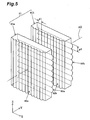
- FIG. 5 is a perspective view schematically showing a construction of the cylindrical micro fly's eye lens according to the first modification of the embodiment.
- a cylindrical micro fly's eye lens 81 is constructed from a first fly's eye member 81a arranged on the light source side and a second fly's eye member 81b arranged on the mask side.
- Cylindrical lens groups 82a and 82b arranged along the X direction are formed with a pitch of p1 respectively on each light source side of the first fly's eye member 81a and the second fly's eye member 81b.
- cylindrical lens groups 83a and 83b arranged along the Z direction are formed with a pitch of p2 respectively on each mask side of the first fly's eye member 81a and the second fly's eye member 81b.
- a wavefront of a parallel light beam entering along the optical axis AX is segmentalized with the pitch of p1 along the X direction by the cylindrical lens group 82a formed on the light source side of the first fly's eye member 81a. Then, the light beam receives condensing action on the refraction surface thereof.
- the light beam receives condensing action on a refraction surface of a corresponding cylindrical lens among the cylindrical lens group 82b formed on the light source side of the second fly's eye member 81b. Then, the light beam focuses on the rear side focal surface of the cylindrical micro fly's eye lens 81.
- a wavefront of a parallel light beam entering along the optical axis AX is segmentalized with a pitch of p2 along the Z direction by the cylindrical lens group 83a formed on the mask side of the first fly's eye member 81a. Then the light beam receives condensing action on the refraction surface thereof. After that, the light beam receives condensing action on a refraction surface of a corresponding cylindrical lens among the cylindrical lens group 83b formed on the mask side of the second fly's eye member 81b. Then, the light beam focuses on the rear side focal surface of the cylindrical micro fly's eye lens 81.
- the cylindrical micro fly's eye lens 81 of the first modification is constructed from the first fly's eye member 81a and the second fly's eye member 81b, wherein each cylindrical lens group is arranged on the both sides.
- the cylindrical micro fly's eye lens 81 demonstrates an optical function similar to of the micro fly's eye lens 8 constructed from the first fly's eye member 8a and the second fly's eye member 8b, wherein many minute refraction surfaces having the size of p1 in the X direction and the size of p2 in the Z direction are vertically and horizontally and integrally formed.
- the refraction surfaces of the cylindrical lens group 82a formed on the light source side of the first fly's eye member 81a construct the first minute refraction surfaces
- the refraction surfaces of the cylindrical lens group 82b formed on the light source side of the second fly's eye member 81b construct the second minute refraction surfaces.
- the refraction surfaces of the cylindrical lens group 83a formed on the mask side of the first fly's eye member 81a construct the first minute refraction surfaces
- the refraction surfaces of the cylindrical lens group 83b formed on the mask side of the second fly's eye member 81b construct the second minute refraction surfaces.
- nb the refraction index of the optical material forming the second fly's eye member 81b is set larger than na, the refraction index of the optical material forming the first fly's eye member 81a, and the absolute value of the parameter ⁇ is set lower than 0.2.
- the invention is applied to the micro fly's eye lens 8 constructed from the pair of fly's eye members 8a and 8b.
- application is not limited thereto. It is possible to adopt a modification (second modification), wherein the invention is applied to an ordinary micro fly's eye lens constructed from a single optical member.
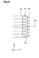
- FIG. 6 is a view schematically showing a construction of the micro fly's eye lens according to the second modification of this embodiment.
- micro fly's eye lens 84 constructed from a single optical member as shown in FIG. 6, many first minute refraction surfaces 84a are formed vertically and horizontally and integrally on the light source side thereof, and many second minute refraction surfaces 84b are formed vertically and horizontally and integrally on the mask side thereof so that many second minute refraction surfaces 84b optically correspond to many first minute refraction surfaces 84a.
- the micro fly's eye lens 84 is bisected by a virtual segmentation surface 84c perpendicular to the optical axis AX. Then, it is regarded that a portion on the light source side from the segmentation surface 84c constructs the first optical member, and a portion on the mask side from the segmentation surface 84c constructs the second optical member.
- the micro fly's eye lens 84 is constructed from the single optical member. Therefore, differently from the foregoing embodiment, it is not possible to set a refraction index of an optical material forming the second optical member larger than a refraction index of an optical material forming the first optical member. However, similarly to in the foregoing embodiment, in the second modification, change of the distortion aberration caused by variations of surface shapes of the minute refraction surfaces of the micro fly's eye lens 84 can be reduced, and effects on the illumination intensity distribution can be reduced by setting the absolute value of the parameter ⁇ lower than 0.2.
- the refracting power ratio ⁇ and the refraction index difference ⁇ n do not depend on the directions but are constant, and the numerical aperture NA on the emission side in the nonscanning direction (Z direction) is set larger than in the scanning direction (X direction). Therefore, when setting is made so that the conditional formula of the parameter ⁇ is satisfied in terms of the nonscanning direction (Z direction) according to the invention, the conditional formula of the parameter ⁇ in terms of the scanning direction (X direction) is consequentially satisfied as well.
- the refraction index difference ⁇ n does not depend on the directions but is constant, and the numerical aperture NA on the emission side in the nonscanning direction is set larger than in the scanning direction.
- the refracting power ratio ⁇ does not depend directions, and can be set freely to some extent. Therefore, in this case, such an aspect can be adopted that the conditional formula of the parameter ⁇ is satisfied in terms of the nonscanning direction (Z direction), but the conditional formula of the parameter ⁇ in terms of the scanning direction (X direction) is not always satisfied.
- a micro device semiconductor device, image pickup device, liquid crystal display device, thin film magnetic head and the like
- a micro device can be manufactured by illuminating the mask (reticle) by the illumination optical device (illumination step), and exposing the pattern for transfer formed on the mask on the photosensitive substrate by using the projection optical system (exposure step).
- illumination optical device illumination optical device
- exposure step exposing the pattern for transfer formed on the mask on the photosensitive substrate by using the projection optical system
- Step 301 of FIG. 7 a metal film is deposited on one lot of wafer.
- the metal film on the one lot of wafer is coated with photoresist.
- Step 303 an image of a pattern on the mask is sequentially exposed and transferred in each shot region on the one lot of wafer through the projection optical system by using the exposure apparatus of the foregoing embodiment.
- Step 304 the photoresist on the one lot of wafer is developed.
- Step etching is performed by using the resist pattern as a mask on the one lot of wafer. Thereby, a circuit pattern corresponding to the pattern on the mask is formed in each shot region on each wafer.
- a circuit pattern of an upper layer is further formed, and thereby the device such as the semiconductor device is manufactured.
- the foregoing method of manufacturing semiconductor devices it is possible to obtain a semiconductor device having a very fine circuit pattern with good throughput.
- a liquid crystal display device as a micro device can be also obtained by forming a given pattern (circuit pattern, electrode pattern and the like) on a plate (glass substrate).
- a given pattern circuit pattern, electrode pattern and the like
- a plate glass substrate.
- photolithography step so-called photolithography step, wherein a pattern of a mask is transferred and exposed on a photosensitive substrate (glass substrate or the like coated with resist) by using the exposure apparatus of the foregoing embodiment is performed.
- a given pattern including many electrodes and the like is formed on the photosensitive substrate.
- the exposed substrate is provided with respective steps such as development step, etching step, and resist exfoliation step. Thereby, a given pattern is formed on the substrate.
- the procedure is forwarded to the next color filter formation step 402.
- a color filter wherein many groups constructed from three dots corresponding to R (Red), G (Green), and B (Blue) are arranged in a state of a matrix, or a color filter wherein a plurality of filter groups constructed from three stripes of R, G, and B are arranged in the direction of horizontal scanning line is formed.
- cell assembly step 403 is performed.
- a liquid crystal panel liquid crystal cell
- the liquid crystal panel is manufactured by, for example, injecting liquid crystal between the substrate having the given pattern obtained in the pattern formation step 401 and the color filter obtained in the color filter formation step 402.
- module assembly step 404 respective parts such as an electric circuit for making display operation of the assembled liquid crystal panel (liquid crystal cell) and a backlight are installed to complete the liquid crystal display device.
- respective parts such as an electric circuit for making display operation of the assembled liquid crystal panel (liquid crystal cell) and a backlight are installed to complete the liquid crystal display device.
- the mask M is illuminated in a state of superimposition by condensing light from the secondary light source by the condenser optical system.
- the invention is not limited thereto. It is possible that an illumination field stop (mask blind) and a relay optical system for forming an image of this illumination field stop on the mask M are arranged in the optical path between the condenser optical system 9 and the mask M.
- the condenser optical system 9 condenses light from the secondary light source for illuminating the illumination field stop in a state of superimposition.
- the relay optical system forms the image of an aperture part (light transmittance part) of the illumination field stop on the mask M.
- the KrF excimer laser light (wavelength: 248 nm) or the ArF excimer laser light (wavelength: 193 nm) is used as exposure light.
- the invention is not limited thereto.
- the invention can be also applied to, for example, exposure light having a wavelength of 300 nm or less.
- the invention has been described taking the example of the projection exposure apparatus comprising the illumination optical device. However, it is clear that the invention can be applied to a general illumination optical device for illuminating irradiated surfaces other than the mask.
- an optical integrator is set to satisfy a conditional formula in terms of a parameter ⁇ . Therefore, change of a distortion aberration caused by variations of surface shapes of minute refraction surfaces of the optical integrator can be reduced, and then effects on an illumination intensity distribution on an irradiated surface can be reduced.
- an illumination optical device of the invention it is possible to illuminate the irradiated surface under desired illumination conditions by using the optical integrator, wherein effects of manufacturing errors of the minute refraction surfaces on the illumination intensity distribution are reduced. Further, in an exposure apparatus and an exposure method of the invention, a good device can be manufactured by performing good projection exposure under good illumination conditions by using the highly efficient illumination optical device capable of illuminating the irradiated surface under the desired illumination conditions.
Landscapes
- Physics & Mathematics (AREA)
- General Physics & Mathematics (AREA)
- Optics & Photonics (AREA)
- Exposure And Positioning Against Photoresist Photosensitive Materials (AREA)
- Exposure Of Semiconductors, Excluding Electron Or Ion Beam Exposure (AREA)
- Lenses (AREA)
- Microscoopes, Condenser (AREA)
Abstract
An optical integrator having characteristics to
reduce effects of manufacturing errors of many minute
refraction surfaces integrally formed by, for example,
etching on an illumination intensity distribution. An
optical integrator (8) comprising an integrally formed
plurality of first minute refraction surfaces (80a) and
an integrally formed plurality of second minute
refraction surfaces (80b). A parameter β satisfies
conditions, |β|<0.2 (where β=(γ-1)3· NA2/Δn2), where a
refracting power ratio ϕa/ϕb between ϕa, a refracting
power of the first minute refraction surfaces and ϕb, a
refracting power of the second minute refraction
surfaces is γ, numerical aperture on an emission side
of the optical integrator is NA, and a difference
between a refraction index of a medium on a light
entrance side of the second minute refraction surfaces
and a refraction index of a medium on a light emission
side of the second minute refraction surfaces is Δn.
Description
The present invention relates to an optical
integrator, an illumination optical device, an exposure
apparatus, and an exposure method, and more
particularly to an illumination optical device suitable
for an exposure apparatus for manufacturing micro
devices such as a semiconductor device, an image pickup
device, a liquid crystal display device, and a thin
film magnetic head in a lithography step.
In a typical exposure apparatus of this kind, a
light beam emitted from a light source enters a fly's
eye lens. Then, a secondary light source constructed
from many light sources is formed on the rear side
focal surface thereof. A light beam from the secondary
light source is limited through an aperture stop
arranged in the vicinity of the rear side focal surface
of the fly's eye lens, and then, enters a condenser
lens. The aperture stop limits a shape or a size of
the secondary light source to a desired shape or a
desired size according to desired illumination
conditions (exposure conditions).
A light beam condensed by the condenser lens
illuminates in a state of superimposition a mask in
which a given pattern is formed. Light passing through
the pattern of the mask forms an image on a wafer
through a projection optical system. Thereby, the mask
pattern is projected and exposed (transferred) on the
wafer. The pattern formed on the mask is highly
integrated. Therefore, in order to correctly transfer
this fine pattern on the wafer, it is essential to
obtain a uniform illumination intensity distribution on
the wafer.
In the exposure apparatus having the foregoing
construction, it is necessary to set minute lens
elements constructing the fly's eye lens as much as
possible in order to improve uniformity of the
illumination intensity distribution. Further, it is
necessary to form the secondary light source in the
shape close to a desired shape in order to avoid light
amount loss in the aperture stop. Therefore, for
example, it is thinkable that a size of the minute lens
element constructing the fly's eye lens is set very
small, that is, a micro fly's eye lens is used.
The fly's eye lens is constructed by arranging
many lens elements vertically and horizontally and
densely. Meanwhile, the micro fly's eye lens is
constructed by integrally forming many minute
refraction surfaces. That is, the fly's eye lens is
constructed by combining and densely arranging many
single polished lens elements. Meanwhile, the micro
fly's eye lens is constructed by forming many minute
refraction surfaces on, for example, a parallel plane
glass plate by applying MEMS technique (lithography
plus etching and the like).
Therefore, the fly's eye lens can be manufactured
by checking refraction surface shapes of polished lens
elements, selecting lens elements meeting standards,
and using only lens elements having a high-precisely
formed refraction surface. However, in the micro fly's
eye lens, all minute refraction surfaces are required
to be concurrently manufactured by etching through
which is hard to obtain a quality surface shape
compared to polishing. Therefore, a straight pass
ratio thereof becomes considerably lower than that of
the fly's eye lens.
In view of the foregoing problem, it is an object
of the invention to provide an optical integrator
having characteristics to reduce the effects of
manufacturing errors of many minute refraction surfaces
integrally formed by etching or the like on an
illumination intensity distribution. Further, it is
another object of the invention to provide a highly
efficient illumination optical device capable of
illuminating an irradiated surface under desired
illumination conditions by using the optical integrator,
wherein the effects of the manufacturing errors of the
minute refraction surfaces on the illumination
intensity distribution are reduced. Further, it is
still another object of the invention to provide an
exposure apparatus and an exposure method capable of
performing good projection exposure under good
illumination conditions by using the highly efficient
illumination optical device capable of illuminating the
irradiated surface under the desired illumination
conditions.
In order to solve the foregoing problem, a first
invention of the present invention provides an optical
integrator, comprising:
According to a preferable aspect of the first
invention, the plurality of first minute refraction
surfaces and the plurality of second minute refraction
surfaces are formed on the same optical member.
Otherwise, the optical integrator comprises: a first
optical member having the plurality of first minute
refraction surfaces; and a second optical member having
the plurality of second minute refraction surfaces
arranged on a light emission side of the first optical
member. Further, according to the preferable aspect of
the first invention, the plurality of second minute
refraction surfaces comprise aspherical surfaces.
A second invention of the present invention
provides an optical integrator, comprising in the order
from a light entrance side:
According to a preferable aspect of the second
invention, the optical integrator satisfies a condition,
0.05≦nb-na, where the refraction index of the optical
material forming the first optical member is na, and
the refraction index of the optical material forming
the second optical member is nb. Further, it is
preferable that the optical integrator is used for
light having a wavelength of 300 nm or less, and the
optical material forming the first optical member
includes silica glass or fluorite, and the optical
material forming the second optical member includes one
material of magnesium oxide, ruby, sapphire, quartz
crystal, and silica glass. Otherwise, it is preferable
that the optical integrator is used for light having a
wavelength of 300 nm or less, and the optical material
forming the first optical member includes fluorite, and
the optical material forming the second optical member
includes silica glass. Further, in the first invention
and the second invention, it is preferable that each
minute refraction surface is formed spherically or
aspherically. Further, it is preferable that this
aspherical surface is a rotational symmetry aspherical
surface or a rotational asymmetry aspherical surface
(for example, a cylindrical surface).
A third invention of the present invention
provides an illumination optical device for
illuminating an irradiated surface, comprising: the
optical integrator of the first invention or the second
invention. In this case, it is preferable that the
optical integrator forms a light intensity distribution
in a given shape in an illumination region.
A fourth invention of the present invention
provides an exposure apparatus, comprising: the
illumination optical device of the third invention; and
a projection optical system for projecting and exposing
a pattern of a mask arranged on the irradiated surface
on a photosensitive substrate.
According to a preferable aspect of the fourth
invention, the pattern of the mask is projected and
exposed on the photosensitive substrate by relatively
moving the mask and the photosensitive substrate in
relation to the projection optical system along a
scanning direction, and an absolute value of the
parameter β in terms of a direction optically
approximately perpendicular to the scanning direction
is set lower than an absolute value of the parameter β
in terms of the scanning direction.
A fifth invention of the present invention
provides an exposure method, wherein a mask is
illuminated through the illumination optical device of
the third invention, and wherein an image of a pattern
formed on the illuminated mask is projected and exposed
on a photosensitive substrate.
A sixth invention of the present invention
provides an exposure apparatus, comprising:
FIG. 1 is a view explaining a basal principle of
the invention. Referring to FIG. 1, light supplied
from a light source S provides Koehler illumination for
a micro fly's eye lens MF through a first condenser
optical system C1. The micro fly's eye lens MF
comprises a first subsystem A and a second subsystem B
in the order from the light source S side. Many first
minute refraction surfaces are integrally formed in the
first subsystem A, and many second minute refraction
surfaces are integrally formed in the second subsystem
B so that the second minute refraction surfaces
optically correspond to the first minute refraction
surfaces.
Therefore, light whose wavefront is segmented by
the respective minute refraction surfaces of the micro
fly's eye lens MF reaches an illumination field I on an
irradiated surface through a second condenser optical
system C2. Here, an optical conjugate relation is
established between an entrance surface A1 of the micro
fly's eye lens MF (that is, an entrance surface of the
first subsystem A) and the illumination field I.
Therefore, a light intensity distribution in a region
corresponding to each minute refraction surface on the
entrance surface A1 is respectively expanded and
projected on the whole illumination field I. FIG. 1
shows a model of only light ray corresponding to one
minute refraction surface. However, in practice, the
whole illumination field I is illuminated in a state of
superimposition through many minute refraction surfaces,
and thereby uniformity of illumination intensity can be
obtained over the whole illumination field I.
In the illumination system shown in Fig. 1, there
is the conjugate relation between the entrance surface
A1 of the micro fly's eye lens MF and the illumination
field I. However, when a distortion aberration of an
imaging system P (micro fly's eye lens MF plus second
condenser optical system C2) is changed, an imaging
magnification varies according to an image height.
Therefore, the illumination intensity distribution in
the illumination field I becomes changed. For example,
according to Isshiki Masaki, "Image Surface
Illumination Intensity Distribution of Photographic
Lens", Optical Technology Contact Vol. 5, No. 11, pp.
10-14, 1967, it is known that when the distortion
aberration of the imaging system P is changed by D%,
the illumination intensity in the illumination field
(image surface of the imaging system P) I is changed by
about 4D%.
As an evaluation method for the aberration of the
imaging system (including the distortion aberration),
aberration evaluation method by third order aberration
theory is known. Analysis of the aberration by the
third order aberration theory has an advantage that
evaluation is facilitated since analytical calculation
is enabled in spite of errors due to approximation.
Details of derivation method of an aberration
coefficient by the third order aberration theory are,
for example, described in Matsui Yoshiya, "Aberration
Theory," Japan Optoelectro Mechanics Association, 1989.
Discussion will be hereinafter given of change of the
distortion aberration of the imaging system P lying
between the entrance surface A1 of the micro fly's eye
lens MF and the illumination field I when surface
shapes of the minute refraction surfaces of the micro
fly's eye lens MF are changed by using the third order
aberration theory.
A surface shape of each minute refraction surface
in the micro fly's eye lens MF is expressed by the
following Formula (1), where a height in the direction
perpendicular to an optical axis is y, a distance (sag
amount) along the optical axis between a tangent plane
on the top of the refraction surface and a position on
the refraction surface in the height y is x, a
curvature is c, and a conic coefficient is K.
x=(c· y2 )/[1+{1-(x+1)c2 · y2 }1/2 ]
According to the third order aberration theory,
any aberration coefficient can be expressed by a sum of
a spheric term and an aspheric term. Variations of
surface shapes in manufacturing the micro fly's eye
lens MF appear as change of the curvature c and the
conic coefficient κ in the foregoing formula (1). Here,
the change of the curvature c affects a size of
illumination, but does not affect illumination
nonuniformity practically. Meanwhile, the change of
the conic coefficient κ changes the aspheric term of
the aberration coefficient, and affects the
illumination nonuniformity.
According to the foregoing Matsui Yoshiya,
"Aberration Theory", Vasp, an aspheric term of the
distortion aberration coefficient of object imaging is
generally expressed by the following Formula (2). In
Formula (2), hi represents a light ray height of an
image paraxial tracing value (light ray height in
tracing an object (image) paraxial ray (paraxial ray
related to the object (the image))), and hp represents
a light ray height of a pupil paraxial tracing value
(light ray height in tracing a pupil paraxial ray
(paraxial ray related to the pupil)). Ψ represents a
coefficient expressed by the next Formula (3).
Vasp = hi · hp 3 · Ψ
Ψ=Δn· c3 · K
Here, Δn represents a difference between a
refraction index of a medium on the light entrance side
of the minute refraction surfaces and a refraction
index of a medium on the light emission side of the
minute refraction surfaces. Δn represents a value
obtained by subtracting n1, a refraction index of the
medium on the light entrance side of the minute
refraction surfaces from n2, a refraction index of the
medium on the light emission side of the minute
refraction surfaces (n2-n1). FIG. 2 is a view
explaining optical characteristics in the micro fly's
eye lens of FIG. 1. In FIG. 2, a refracting power
(power) of the micro fly's eye lens MF is expressed by
ϕ, a refracting power of the first subsystem A is
expressed by ϕa, a refracting power of the second
subsystem B is expressed by ϕb, and an air conversion
surface-to-surface distance between the first subsystem
A and the second subsystem B is expressed by s.
Therefore, relations shown in the following
Formulas (4a) to (4d) are established, where ϕ, the
refracting power of the micro fly's eye lens MF is
standardized to 1, and a refracting power ratio ϕa/ϕb
between ϕa, the refracting power of the first subsystem
A and ϕb, the refracting power of the second subsystem
B is γ.
ϕ=1
ϕa=γ
ϕb=1
s=1
Paraxial tracing values then are shown in the
following Table 1.
| Height of ray related to the image hi | Image conversion obliquity αi | Height of ray related to the pupil hp | Pupil conversion obliquity αp | |
| First subsystem A | 0 | -1 | -1 | 0 |
| Second subsystem B | 1 | -1 | γ-1 | -γ |
Referring to Table 1 and Formulas (2) and (3),
VaspA, an aspheric term of the distortion aberration
coefficient in the first subsystem A and VaspB, an
aspheric term of the distortion aberration coefficient
in the second subsystem B are expressed by the
following Formulas (5) and (6) respectively.
VaspA =0
VaspB =(γ-1)3 · Δn· c3 · κ
Referring to Formulas (5) and (6), it is found
that change of the aspheric term of the distortion
aberration coefficient caused by variations of surface
shapes of the minute refraction surfaces of the micro
fly's eye lens MF (that is, change of the conic
coefficient κ) is generated only in the second
subsystem B in the range of the third order aberration.
Next, discussions will be given of effects of the
change of the aspheric term of the distortion
aberration coefficient on the illumination intensity
distribution in the illumination field I. In the
second subsystem B, the proportionality relation shown
in the following Formula (7) is established between the
curvature c and the refraction index difference Δn.
c∝ 1/Δn
In the range of the third order aberration, the
illumination intensity distribution in the illumination
field I is changed in proportion to a square value of
the image height. The image height is proportional to
numerical aperture NA on the emission side of the micro
fly's eye lens MF. Therefore, based on Formulas (5) to
(7), change of the distortion aberration caused by
change of surface shapes of the minute refraction
surfaces of the micro fly's eye lens MF, then β,
sensitivity of change of the illumination intensity
distribution on the illumination field (image surface)
I is expressed by the following Formula (8).
β=(γ-1)3 · NA2 /Δn2
When the micro fly's eye lens MF is arranged in
the air, Formula (8) can be transformed into the
following Formula (8'), where a refraction index of an
optical material forming the second subsystem B is n.
β=(γ-1)3 · NA2 /(n-1)2
Thereby, it is possible to reduce change of the
distortion aberration caused by variations of surface
shapes of the minute refraction surfaces of the micro
fly's eye lens MF, and to reduce effects on the
illumination intensity distribution in the illumination
field I by reducing an absolute value of the parameter
β. In other words, it is possible to realize a micro
fly's eye lens (optical integrator) MF having
characteristics, wherein effects of manufacturing
errors of many minute refraction surfaces integrally
formed by etching or the like on the illumination
intensity distribution are reduced by reducing the
absolute value of the parameter β.
Referring to Formula (8), it is thinkable that
the absolute value of the parameter β can be reduced by
increasing the refracting power ratio γ, increasing the
refraction index difference Δn, and reducing the
numerical aperture NA on the emission side of the micro
fly's eye lens MF. However, when the refracting power
ratio γ is increased and gets close to 1, the risk that
an energy density on an entrance surface B2 of the
micro fly's eye lens MF (that is, emission surface of
the second subsystem B) is increased and then the
second subsystem B is damaged by light energy
irradiation becomes increased.
Further, the numerical aperture NA on the
emission side of the micro fly's eye lens MF is
determined by a size of an illumination region and a
focal length of the second condenser optical system C2.
In general, there is no design flexibility to set the
numerical aperture NA on the emission side of the micro
fly's eye lens MF to a desired small value without
changing the size of the illumination region and the
focal length of the second condenser optical system C2.
In result, in the invention, such a technique is
adapted that the refraction index difference Δn in the
second subsystem B is set large. However, the cost is
easily increased along with increase of the refraction
index of the optical material. Therefore, it is
realistic that an optical material having a high
refraction index is used only for the second subsystem
B.
Therefore, in the invention, nb, a refraction
index of an optical material forming the second
subsystem B (second optical member) is set larger than
na, a refraction index of an optical material forming
the first subsystem A (first optical member). In this
case, in order to well demonstrate effects of the
invention, it is preferable that the refraction index
na and the refraction index nb satisfy a condition of
0.05≦nb-na. More specifically, when the first
subsystem A is formed by silica glass or fluorite, it
is preferable that the second subsystem B is formed by
magnesium oxide, ruby, sapphire, quartz crystal, or
silica glass. When the first subsystem A is formed by
fluorite, it is preferable that the second subsystem B
is formed by silica glass.
According to a simulation based on a design
numerical value example, in the case of a typical micro
fly's eye lens MF, wherein a size (dimension) of each
minute refraction surface is 0.7 mm and numerical
aperture NA on the emission side is 0.25, it was found
that it was difficult to obtain a surface shape error
of the minute refraction surfaces of 50 nm or less, and
in this case, when the absolute value of the parameter
β was larger than 0.2, variations of illumination
intensity in the illumination field (image surface) I
tended to become large as much as intolerable.
Therefore, in the invention, change of the
distortion aberration caused by variations of surface
shapes of the minute refraction surfaces of the micro
fly's eye lens MF is reduced, and then effects on the
illumination intensity distribution in the illumination
field I are reduced by setting the absolute value of
the parameter β lower than 0.2. In order to further
reduce effects of the manufacturing error of the minute
refraction surfaces on the illumination intensity
distribution, it is preferable that the upper limit
value of the absolute value of the parameter β is set
to 0.13. In some cases, it is necessary to highly
control the illumination intensity distribution in the
illumination region in the illumination system. In
this case, it is preferable that the absolute value of
the parameter β is set lower than 0.2, and the minute
refraction surfaces of the second subsystem B are
aspheric. Thereby, it becomes possible to control the
distortion aberration of the imaging system P (micro
fly's eye lens MF plus second condenser optical system
C2). Then, it becomes possible to approximate the
illumination intensity distribution in the illumination
region to a desired distribution.
An embodiment of the invention will be described
with reference to the attached drawings.
FIG. 3 is a view schematically showing a
construction of an exposure apparatus comprising an
illumination optical device according to the embodiment
of the invention. In FIG. 3, Z axis is set along the
normal line of a wafer W, a photosensitive substrate, Y
axis is set in the direction parallel to a paper space
of FIG. 3 in a wafer face, and X axis is set in the
direction perpendicular to the paper space of FIG. 3 in
the wafer face respectively. In FIG. 3, the
illumination optical device is set to perform annular
illumination.
The exposure apparatus of FIG. 3 comprises, for
example, a KrF excimer laser light source for supplying
light having a wavelength of 248 nm, or an ArF excimer
laser light source for supplying light having a
wavelength of 193 nm as a light source 1. An almost
parallel light beam emitted from the light source 1
along the Z direction has a rectangular cross section
longly extending along the X direction. The light beam
enters a beam expander 2 constructed from a pair of
lenses 2a and 2b. The respective lenses 2a and 2b have
a negative refracting power and a positive refracting
power in the paper space (YZ plain) of FIG. 3
respectively. Therefore, the light beam entering the
beam expander 2 is expanded in the paper space of FIG.
3, and shaped into a light beam having a given
rectangular cross section.
An almost parallel light beam through the beam
expander 2 as a optical shaping system is deflected in
the Y direction by a deflecting mirror 3, and then
enters an afocal zoom lens 5 through a diffractive
optical element 4. In general, the diffractive optical
element is constructed by forming steps having a pitch
of about a wavelength of exposure light (illumination
light) on a glass substrate. The diffractive optical
element has an action for diffracting an incident beam
at a desired angle. More specifically, when a parallel
light beam having a rectangular cross section enters
the diffractive optical element 4, the diffractive
optical element 4 has a function to form a circular
light intensity distribution in a far field thereof (or
Fraunhofer diffraction region). Therefore, the light
beam through the diffractive optical element 4 forms
the circular light intensity distribution, that is, a
light beam having a circular cross section in the
position of a pupil of the afocal zoom lens 5.
The diffractive optical element 4 is constructed
to be able to retreat from an illumination optical path.
The afocal zoom lens 5 is constructed to be able to
continuously change magnifications in a given range
while maintaining an afocal system (afocal optical
system). A light beam through the afocal zoom lens 5
enters a diffractive optical element 6 for annular
illumination. The afocal zoom lens 5 optically and
almost conjugately connects a divergence original point
of the diffractive optical element 4 and a diffractive
surface of the diffractive optical element 6.
Numerical aperture of the light beam focusing on one
point of the diffractive surface of the diffractive
optical element 6 or the surface in the vicinity
thereof varies according to magnifications of the
afocal zoom lens 5.
When a parallel light beam enters the diffractive
optical element 6 for annular illumination, the
diffractive optical element 6 for annular illumination
has a function to form a ring light intensity
distribution in a far field thereof. The diffractive
optical element 6 is constructed removably from the
illumination optical path. In addition, the
diffractive optical element 6 is constructed changeably
with a diffractive optical element 60 for quadrupole
illumination or a diffractive optical element 61 for
circular illumination. A light beam through the
diffractive optical element 6 enters a zoom lens 7. In
the vicinity of a rear side focal surface of the zoom
lens 7, an entrance surface of a micro fly's eye lens 8
constructed from a first fly's eye member 8a and a
second fly's eye member 8b in the order from the light
source side (that is, entrance surface of the first
fly's eye member 8a) is positioned. The micro fly's
eye lens 8 functions as an optical integrator forming
many light sources based on the incident light beam.
Its detailed construction and action will be described
later.
As described above, the light beam from the
circular light intensity distribution formed in the
position of the pupil of the afocal zoom lens 5 through
the diffractive optical element 4 is emitted from the
afocal zoom lens 5. After that, the emitted light beam
becomes a light beam having various angle elements,
which enters the diffractive optical element 6.
Therefore, the light beam through the diffractive
optical element 6 forms, for example, an annular
illumination field centering on an optical axis AX on
the rear side focal surface of the zoom lens 7 (then on
the entrance surface of the micro fly's eye lens 8).
An outer diameter of the annular illumination
field formed on the entrance surface of the micro fly's
eye lens 8 varies according to focal lengths of the
zoom lens 7. Therefore, the zoom lens 7 practically
connects the diffractive optical element 6 and the
entrance surface of the micro fly's eye lens 8 in a
state of Fourier transformation relation. A light beam
entering the micro fly's eye lens 8 is segmentalized
two-dimensionally. Many light sources (hereinafter
referred to as "secondary light source") in the same
annular state as in the illumination field formed by
the incident light beam are formed on the rear side
focal surface thereof.
A light beam from the annular secondary light
source formed on the rear side focal surface of the
micro fly's eye lens 8 receives a condensing action of
a condenser optical system 9, and then illuminates in a
state of superimposition a mask M, wherein a given
pattern is formed. A light beam passing through the
pattern of the mask M forms an image of the mask
pattern on the wafer W, the photosensitive substrate
through a projection optical system PL. Thereby, the
pattern of the mask M is sequentially exposed in each
exposure region of the wafer W by performing exposure
in batch or scanning exposure while two-dimensionally
drive-controlling the wafer W in the plane (XY plane)
perpendicular to the optical axis AX of the projection
optical system PL.
In the exposure in batch, the mask pattern is
exposed in batch for each exposure region of the wafer
according to so-called step and repeat method. In this
case, a shape of the illumination region on the mask M
is a rectangle close to a square. Meanwhile, in the
scanning exposure, the mask pattern is scanned and
exposed for each exposure region of the wafer while the
mask and the wafer are relatively moved in relation to
the projection optical system according to so-called
step and scanning method. In this case, a shape of the
illumination region on the mask M is a rectangle,
wherein a ratio between a short side and a long side is,
for example, 1:3.
In this embodiment, when a magnification of the
afocal zoom lens 5 is changed, a center height of the
annular secondary light source(distance between a
center line of the circle and the optical axis AX.) is
not changed, but only a width thereof (1/2 of a
difference between an outer diameter (diameter) and an
internal diameter (diameter)) is changed. That is, it
is possible to change both a size (outer diameter) and
a shape (annular ratio: internal diameter/outer
diameter) of the annular secondary light source by
changing magnifications of the afocal zoom lens 5.
Further, when the focal length of the zoom lens 7
is changed, the annular ratio of the annular secondary
light source is not changed, but both the center height
and the width thereof are changed. That is, it is
possible to change an outer diameter of the annular
secondary light source without changing the annular
ratio thereof by changing the focal length of the zoom
lens 7. Therefore, in this embodiment, only the
annular ratio of the annular secondary light source can
be changed without changing the outer diameter thereof
by changing magnifications of the afocal zoom lens 5
and focal lengths of the zoom lens 7 as appropriate.
As described above, the diffractive optical
element 6 is constructed removably from the
illumination optical path. In addition, the
diffractive optical element 6 is constructed changeably
with the diffractive optical element 60 for quadrupole
illumination or the diffractive optical element 61 for
circular illumination. Description will be hereinafter
given of the quadrupole illumination obtained by
setting the diffractive optical element 60 in the
illumination optical path instead of the diffractive
optical element 6. When a parallel light beam enters
the diffractive optical element 60 for quadrupole
illumination, the diffractive optical element 60 for
quadrupole illumination has a function to form a four
point light intensity distribution in a far field
thereof. Therefore, a light beam through the
diffractive optical element 60 forms a quadrupole
illumination field constructed from four circular
illumination fields centering on, for example, the
optical axis AX on the entrance surface of the micro
fly's eye lens 8. In result, the same quadrupole
secondary light source as in the illumination field
formed on the entrance surface of the micro fly's eye
lens 8 is formed on the rear side focal surface of the
micro fly's eye lens 8.
As in the case of the annular illumination, it is
also possible in the quadrupole illumination that both
an outer diameter of the quadrupole secondary light
source (diameter of a circumscribed circle of four
circular surface light sources) and an annular ratio
thereof (diameter of an inscribed circle of the four
circular surface light sources/diameter of the
circumscribed circle of the four circular surface light
sources) are changed by changing magnifications of the
afocal zoom lens 5. Further, it is possible to change
the outer diameter of the quadrupole secondary light
source without changing the annular ratio thereof by
changing the focal length of the zoom lens 7. In
result, only the annular ratio of the quadrupole
secondary light source can be changed without changing
the outer diameter of the quadrupole secondary light
source by changing magnifications of the afocal zoom
lens 5 and focal lengths of the zoom lens 7 as
appropriate.
Next, descriptions will be given of the circular
illumination obtained by retiring the diffractive
optical element 4 from the illumination optical path
and setting the diffractive optical element 61 for
circular illumination in the illumination optical path
instead of the diffractive optical elements 6 or 60.
In this case, a light beam having a rectangular cross
section enters the afocal zoom lens 5 along the optical
axis AX. The light beam entering the afocal zoom lens
5 is expanded or reduced according to the magnification,
is emitted from the afocal zoom lens 5 along the
optical axis AX while being the light beam having the
rectangular cross section as it is, and enters the
diffractive optical element 61.
Here, similarly to the diffractive optical
element 4, when a parallel light beam having a
rectangular cross section enters the diffractive
optical element 61 for circular illumination, the
diffractive optical element 61 for circular
illumination has a function to form a circular light
intensity distribution in a far field thereof.
Therefore, the circular light beam formed by the
diffractive optical element 61 forms a circular
illumination field centering on the optical axis AX on
the entrance surface of the micro fly's eye lens 8
through the zoom lens 7. In result, a circular
secondary light source centering on the optical axis AX
is formed on the rear side focal surface of the micro
fly's eye lens 8 as well. In this case, an outer
diameter of the circular secondary light source can be
changed as appropriate by changing magnifications of
the afocal zoom lens 5 or focal lengths of the zoom
lens 7.
FIG. 4 is a view schematically showing a
construction of the micro fly's eye lens of FIG. 3.
Referring to FIG. 4, the micro fly's eye lens 8 is
constructed from the first fly's eye member 8a arranged
on the light source side and the second fly's eye
member 8b arranged on the mask side (irradiated surface
side). Many first minute refraction surfaces 80a are
vertically and horizontally and integrally formed on a
surface on the light source side (left of center in FIG.
4) of the first fly's eye member 8a. Meanwhile, many
second minute refraction surfaces 80b are vertically
and horizontally and integrally formed on a surface on
the mask side of the second fly's eye member 8b so that
the second minute refraction surfaces 80b optically
correspond to many first minute refraction surfaces 80a.
Here, each minute refraction surface is formed
spherically, and has a rectangular outer shape similar
to the illumination region to be formed on the mask M.
Therefore, a wavefront of a parallel light beam
entering the micro fly's eye lens 8 is segmentalized by
many first minute refraction surfaces 80a. Then, the
parallel light beam sequentially receives refraction
actions of the first minute refraction surfaces 80a and
the corresponding second minute refraction surfaces 80b.
After that, the light beam focuses on a rear side focal
surface 80c of the micro fly's eye lens 8. In result,
many light sources as many as the number of the first
minute refraction surfaces 80a (then the number of the
second minute refraction surfaces 80b) are formed.
In this embodiment, the first fly's eye member 8a
is formed, for example, by silica glass or fluorite,
and the second fly's eye member 8b is formed, for
example, by quartz crystal. Otherwise, the first fly's
eye member 8a is formed, for example, by fluorite, and
the second fly's eye member 8b is formed, for example,
by silica glass. That is, nb, the refraction index of
the optical material forming the second fly's eye
member 8b is set larger than na, the refraction index
of the optical material forming the first fly's eye
member 8a by, for example, 0.05 or more.
Further, in this embodiment, the absolute value
of the parameter β defined by Formula (8) is set lower
than 0.2. Here, the refraction index difference Δn in
Formula (8) is given by a difference between nb, the
refraction index of the optical material forming the
second fly's eye member 8b and nc, a refraction index
of a medium forming an atmosphere of the micro fly's
eye lens 8 (nb-nc). That is, when the micro fly's eye
lens 8 is arranged in the air, the refraction index
difference Δn is given by (nb-1).
In this embodiment, as described above, nb, the
refraction index of the optical material forming the
second fly's eye member 8b is set relatively large.
Therefore, the refraction index difference Δn becomes
large, then the absolute value of the parameter β is
reduced. In result, it is possible to reduce change of
the distortion aberration caused by variations of
surface shapes of the minute refraction surfaces of the
micro fly's eye lens MF, then to reduce effects on the
illumination intensity distribution in the mask M and
the wafer W based on the foregoing actions of the
invention.
In the foregoing embodiment, the invention is
applied to the micro fly's eye lens 8, wherein each
minute refraction surface is formed spherically.
However, application is not limited thereto. Such a
modification (first modification) can be adopted that
the invention is applied to a cylindrical micro fly's
eye lens, wherein each minute refraction surface is
formed cylindrically. FIG. 5 is a perspective view
schematically showing a construction of the cylindrical
micro fly's eye lens according to the first
modification of the embodiment.
Referring to FIG. 5, a cylindrical micro fly's
eye lens 81 according to the first modification of the
embodiment is constructed from a first fly's eye member
81a arranged on the light source side and a second
fly's eye member 81b arranged on the mask side.
Cylindrical lens groups 82a and 82b arranged along the
X direction are formed with a pitch of p1 respectively
on each light source side of the first fly's eye member
81a and the second fly's eye member 81b.
Meanwhile, cylindrical lens groups 83a and 83b
arranged along the Z direction are formed with a pitch
of p2 respectively on each mask side of the first fly's
eye member 81a and the second fly's eye member 81b.
Focusing attention on refraction action in terms of the
X direction of the cylindrical micro fly's eye lens 81
(that is, refraction action in terms of the XY plane),
a wavefront of a parallel light beam entering along the
optical axis AX is segmentalized with the pitch of p1
along the X direction by the cylindrical lens group 82a
formed on the light source side of the first fly's eye
member 81a. Then, the light beam receives condensing
action on the refraction surface thereof. After that,
the light beam receives condensing action on a
refraction surface of a corresponding cylindrical lens
among the cylindrical lens group 82b formed on the
light source side of the second fly's eye member 81b.
Then, the light beam focuses on the rear side focal
surface of the cylindrical micro fly's eye lens 81.
Meanwhile, focusing attention on refraction
action in terms of the Z direction of the cylindrical
micro fly's eye lens 81 (that is, refraction action in
terms of the ZY plane), a wavefront of a parallel light
beam entering along the optical axis AX is
segmentalized with a pitch of p2 along the Z direction
by the cylindrical lens group 83a formed on the mask
side of the first fly's eye member 81a. Then the light
beam receives condensing action on the refraction
surface thereof. After that, the light beam receives
condensing action on a refraction surface of a
corresponding cylindrical lens among the cylindrical
lens group 83b formed on the mask side of the second
fly's eye member 81b. Then, the light beam focuses on
the rear side focal surface of the cylindrical micro
fly's eye lens 81.
As described above, the cylindrical micro fly's
eye lens 81 of the first modification is constructed
from the first fly's eye member 81a and the second
fly's eye member 81b, wherein each cylindrical lens
group is arranged on the both sides. However, the
cylindrical micro fly's eye lens 81 demonstrates an
optical function similar to of the micro fly's eye lens
8 constructed from the first fly's eye member 8a and
the second fly's eye member 8b, wherein many minute
refraction surfaces having the size of p1 in the X
direction and the size of p2 in the Z direction are
vertically and horizontally and integrally formed.
When the invention is applied to the cylindrical
micro fly's eye lens 81 of the first modification,
focusing on the refraction action in terms of the X
direction, the refraction surfaces of the cylindrical
lens group 82a formed on the light source side of the
first fly's eye member 81a construct the first minute
refraction surfaces, and the refraction surfaces of the
cylindrical lens group 82b formed on the light source
side of the second fly's eye member 81b construct the
second minute refraction surfaces. Further, focusing
on the refraction action in terms of the Z direction,
the refraction surfaces of the cylindrical lens group
83a formed on the mask side of the first fly's eye
member 81a construct the first minute refraction
surfaces, and the refraction surfaces of the
cylindrical lens group 83b formed on the mask side of
the second fly's eye member 81b construct the second
minute refraction surfaces.
In the first modification, nb, the refraction
index of the optical material forming the second fly's
eye member 81b is set larger than na, the refraction
index of the optical material forming the first fly's
eye member 81a, and the absolute value of the parameter
β is set lower than 0.2. Thereby, similarly to in the
foregoing embodiment, in the first modification, change
of the distortion aberration caused by variations of
surface shapes of the minute refraction surfaces of the
cylindrical micro fly's eye lens 81 can be reduced, and
effects on the illumination intensity distribution can
be reduced.
Further, in the foregoing embodiment, the
invention is applied to the micro fly's eye lens 8
constructed from the pair of fly's eye members 8a and
8b. However, application is not limited thereto. It
is possible to adopt a modification (second
modification), wherein the invention is applied to an
ordinary micro fly's eye lens constructed from a single
optical member. FIG. 6 is a view schematically showing
a construction of the micro fly's eye lens according to
the second modification of this embodiment.
In an ordinary micro fly's eye lens 84
constructed from a single optical member as shown in
FIG. 6, many first minute refraction surfaces 84a are
formed vertically and horizontally and integrally on
the light source side thereof, and many second minute
refraction surfaces 84b are formed vertically and
horizontally and integrally on the mask side thereof so
that many second minute refraction surfaces 84b
optically correspond to many first minute refraction
surfaces 84a. When the invention is applied to the
micro fly's eye lens 84 of the first modification, the
micro fly's eye lens 84 is bisected by a virtual
segmentation surface 84c perpendicular to the optical
axis AX. Then, it is regarded that a portion on the
light source side from the segmentation surface 84c
constructs the first optical member, and a portion on
the mask side from the segmentation surface 84c
constructs the second optical member.
In the second modification, the micro fly's eye
lens 84 is constructed from the single optical member.
Therefore, differently from the foregoing embodiment,
it is not possible to set a refraction index of an
optical material forming the second optical member
larger than a refraction index of an optical material
forming the first optical member. However, similarly
to in the foregoing embodiment, in the second
modification, change of the distortion aberration
caused by variations of surface shapes of the minute
refraction surfaces of the micro fly's eye lens 84 can
be reduced, and effects on the illumination intensity
distribution can be reduced by setting the absolute
value of the parameter β lower than 0.2.
In the case of a scanning exposure type exposure
apparatus, illumination intensity nonuniformity in the
scanning direction on the wafer W can be reduced by
averaging effects by scanning exposure. Therefore, in
the micro fly's eye lens (8, 81, and 84) used for the
scanning exposure type exposure apparatus, it is not
necessary to satisfy the conditional formula of the
parameter β in terms of the direction (X direction)
optically corresponding to the scanning direction (X
direction) on the wafer W. However, it is necessary to
satisfy the conditional formula of the parameter β in
terms of the direction (Z direction) optically
corresponding to the nonscanning direction (Y
direction) on the wafer W.
However, it is general that in the micro fly's
eye lens (8 and 84), wherein each minute refraction
surface is formed spherically, the refracting power
ratio ϒ and the refraction index difference Δn do not
depend on the directions but are constant, and the
numerical aperture NA on the emission side in the
nonscanning direction (Z direction) is set larger than
in the scanning direction (X direction). Therefore,
when setting is made so that the conditional formula of
the parameter β is satisfied in terms of the
nonscanning direction (Z direction) according to the
invention, the conditional formula of the parameter β
in terms of the scanning direction (X direction) is
consequentially satisfied as well.
Meanwhile, in the cylindrical micro fly's eye
lens 81, wherein each minute refraction surface is
formed cylindrically, it is general that the refraction
index difference Δn does not depend on the directions
but is constant, and the numerical aperture NA on the
emission side in the nonscanning direction is set
larger than in the scanning direction. However, the
refracting power ratio γ does not depend directions,
and can be set freely to some extent. Therefore, in
this case, such an aspect can be adopted that the
conditional formula of the parameter β is satisfied in
terms of the nonscanning direction (Z direction), but
the conditional formula of the parameter β in terms of
the scanning direction (X direction) is not always
satisfied.
In the exposure apparatus in the foregoing
embodiment (including the modifications), a micro
device (semiconductor device, image pickup device,
liquid crystal display device, thin film magnetic head
and the like) can be manufactured by illuminating the
mask (reticle) by the illumination optical device
(illumination step), and exposing the pattern for
transfer formed on the mask on the photosensitive
substrate by using the projection optical system
(exposure step). Descriptions will be hereinafter
given of an example of a technique in obtaining a
semiconductor device as a micro device by forming a
given circuit pattern on a wafer or the like as a
photosensitive substrate by using the exposure
apparatus of the foregoing embodiment with reference to
the flowchart of FIG. 7.
First, in Step 301 of FIG. 7, a metal film is
deposited on one lot of wafer. In the next Step 302,
the metal film on the one lot of wafer is coated with
photoresist. After that, in Step 303, an image of a
pattern on the mask is sequentially exposed and
transferred in each shot region on the one lot of wafer
through the projection optical system by using the
exposure apparatus of the foregoing embodiment. After
that, in Step 304, the photoresist on the one lot of
wafer is developed. Then, in Step 305, etching is
performed by using the resist pattern as a mask on the
one lot of wafer. Thereby, a circuit pattern
corresponding to the pattern on the mask is formed in
each shot region on each wafer. After that, for
example, a circuit pattern of an upper layer is further
formed, and thereby the device such as the
semiconductor device is manufactured. According to the
foregoing method of manufacturing semiconductor devices,
it is possible to obtain a semiconductor device having
a very fine circuit pattern with good throughput.
Further, in the exposure apparatus of the
foregoing embodiment, a liquid crystal display device
as a micro device can be also obtained by forming a
given pattern (circuit pattern, electrode pattern and
the like) on a plate (glass substrate). Descriptions
will be hereinafter given of an example of a technique
used then with reference to the flowchart of FIG. 8.
In FIG. 8, in pattern formation step 401, so-called
photolithography step, wherein a pattern of a mask is
transferred and exposed on a photosensitive substrate
(glass substrate or the like coated with resist) by
using the exposure apparatus of the foregoing
embodiment is performed. By this photolithography step,
a given pattern including many electrodes and the like
is formed on the photosensitive substrate. After that,
the exposed substrate is provided with respective steps
such as development step, etching step, and resist
exfoliation step. Thereby, a given pattern is formed
on the substrate. The procedure is forwarded to the
next color filter formation step 402.
Next, in the color filter formation step 402, a
color filter wherein many groups constructed from three
dots corresponding to R (Red), G (Green), and B (Blue)
are arranged in a state of a matrix, or a color filter
wherein a plurality of filter groups constructed from
three stripes of R, G, and B are arranged in the
direction of horizontal scanning line is formed. Then,
after the color filter formation step 402, cell
assembly step 403 is performed. In the cell assembly
step 403, a liquid crystal panel (liquid crystal cell)
is assembled by using the substrate having the given
pattern obtained in the pattern formation step 401, the
color filter obtained in the color filter formation
step 402 and the like. In the cell assembly step 403,
the liquid crystal panel (liquid crystal cell) is
manufactured by, for example, injecting liquid crystal
between the substrate having the given pattern obtained
in the pattern formation step 401 and the color filter
obtained in the color filter formation step 402.
After that, in module assembly step 404,
respective parts such as an electric circuit for making
display operation of the assembled liquid crystal panel
(liquid crystal cell) and a backlight are installed to
complete the liquid crystal display device. According
to the foregoing method of manufacturing liquid crystal
display devices, it is possible to obtain a liquid
crystal display device having a very fine circuit
pattern with good throughput.
In the foregoing embodiment, the mask M is
illuminated in a state of superimposition by condensing
light from the secondary light source by the condenser
optical system. 9. However, the invention is not
limited thereto. It is possible that an illumination
field stop (mask blind) and a relay optical system for
forming an image of this illumination field stop on the
mask M are arranged in the optical path between the
condenser optical system 9 and the mask M. In this
case, the condenser optical system 9 condenses light
from the secondary light source for illuminating the
illumination field stop in a state of superimposition.
The relay optical system forms the image of an aperture
part (light transmittance part) of the illumination
field stop on the mask M.
Further, in the foregoing embodiment, the KrF
excimer laser light (wavelength: 248 nm) or the ArF
excimer laser light (wavelength: 193 nm) is used as
exposure light. However, the invention is not limited
thereto. The invention can be also applied to, for
example, exposure light having a wavelength of 300 nm
or less. Further, in the foregoing embodiment, the
invention has been described taking the example of the
projection exposure apparatus comprising the
illumination optical device. However, it is clear that
the invention can be applied to a general illumination
optical device for illuminating irradiated surfaces
other than the mask.
As described above, in the invention, an optical
integrator is set to satisfy a conditional formula in
terms of a parameter β. Therefore, change of a
distortion aberration caused by variations of surface
shapes of minute refraction surfaces of the optical
integrator can be reduced, and then effects on an
illumination intensity distribution on an irradiated
surface can be reduced.
Therefore, in an illumination optical device of
the invention, it is possible to illuminate the
irradiated surface under desired illumination
conditions by using the optical integrator, wherein
effects of manufacturing errors of the minute
refraction surfaces on the illumination intensity
distribution are reduced. Further, in an exposure
apparatus and an exposure method of the invention, a
good device can be manufactured by performing good
projection exposure under good illumination conditions
by using the highly efficient illumination optical
device capable of illuminating the irradiated surface
under the desired illumination conditions.
Claims (18)
- An optical integrator, comprising:an integrally formed plurality of first minute refraction surfaces; andan integrally formed plurality of second minute refraction surfaces, which are provided closer to a light emission side than the plurality of first minute refraction surfaces so that the plurality of second minute refraction surfaces optically correspond to the plurality of first minute refraction surfaces, whereina parameter β satisfies the following conditions:
|β|<0.2 (where β=(γ-1)3· NA2/Δn2), wherea refracting power ratio ϕa/ϕb between ϕa, a refracting power of the first minute refraction surfaces and ϕb, a refracting power of the second minute refraction surfaces is γ, numerical aperture on the emission side of the optical integrator is NA, and a difference between a refraction index of a medium on a light entrance side of the second minute refraction surfaces and a refraction index of a medium on a light emission side of the second minute refraction surfaces is Δn. - The optical integrator according to claim 1, wherein the plurality of first minute refraction surfaces and the plurality of second minute refraction surfaces are formed on the same optical member.
- The optical integrator according to claim 1, comprising:a first optical member having the plurality of first minute refraction surfaces; anda second optical member having the plurality of second minute refraction surfaces arranged on a light emission side of the first optical member.
- The optical integrator according to any of claims 1 to 3, wherein the plurality of second minute refraction surfaces comprise aspherical surfaces.
- An optical integrator, comprising in the order from a light entrance side:a first optical member having an integrally formed plurality of first minute refraction surfaces; anda second optical member having an integrally formed plurality of second minute refraction surfaces, which are provided to optically correspond to the plurality of first minute refraction surfaces, whereina refraction index of an optical material forming the second optical member is set larger than a refraction index of an optical material forming the first optical member.
- The optical integrator according to claim 5, satisfying the following condition:
0.05≦nb-na, where
the refraction index of the optical material forming the first optical member is na, and the refraction index of the optical material forming the second optical member is nb. - The optical integrator according to claim 5 or claim 6, which is used for light having a wavelength of 300 nm or less, wherein
the optical material forming the first optical member includes silica glass or fluorite, and wherein
the optical material forming the second optical member includes one material of magnesium oxide, ruby, sapphire, quartz crystal, and silica glass. - The optical integrator according to claim 5 or claim 6, which is used for light having a wavelength of 300 nm or less, wherein
the optical material forming the first optical member includes fluorite, and wherein
the optical material forming the second optical member includes silica glass. - The optical integrator according to any of claims 1 to 8, wherein
each minute refraction surface is formed spherically or aspherically. - The optical integrator according to any of claims 4 to 9, wherein
the aspherical surface is a rotational symmetry aspherical surface or a rotational asymmetry aspherical surface. - The optical integrator according to any of claims 1 to 10, used for
an exposure apparatus, wherein a mask and a photosensitive substrate are relatively moved in relation to a projection optical system along a scanning direction, and thereby a pattern of the mask is projected and exposed on the photosensitive substrate, wherein
an absolute value of the parameter β in terms of a direction optically approximately perpendicular to the scanning direction is set lower than an absolute value of the parameter β in terms of the scanning direction. - An illumination optical device for illuminating an irradiated surface, comprising:the optical integrator according to any of claims 1 to 11.
- The illumination optical device according to claim 12, wherein the optical integrator forms a light intensity distribution in a given shape in an illumination region.
- An exposure apparatus, comprising:the illumination optical device according to claim 12 or claim 13; anda projection optical system for projecting and exposing a pattern of a mask arranged on the irradiated surface on a photosensitive substrate.
- The exposure apparatus according to claim 14, wherein
the pattern of the mask is projected and exposed on the photosensitive substrate by relatively moving the mask and the photosensitive substrate in relation to the projection optical system along a scanning direction, and wherein
an absolute value of the parameter β in terms of a direction optically approximately perpendicular to the scanning direction is set lower than an absolute value of the parameter β in terms of the scanning direction. - An exposure method, wherein
a mask is illuminated through the illumination optical device according to claim 12 or claim 13, and wherein
an image of a pattern formed on the illuminated mask is projected and exposed on a photosensitive substrate. - The exposure method according to claim 16, wherein
the pattern of the mask is projected and exposed on the photosensitive substrate while the mask and the photosensitive substrate are relatively moved in relation to a projection optical system along a scanning direction, and wherein
an absolute value of the parameter β in terms of a direction optically approximately perpendicular to the scanning direction is set lower than an absolute value of the parameter β in terms of the scanning direction. - An exposure apparatus, comprising:an illumination optical system including an optical integrator; anda projection optical system for forming a pattern image of a mask on a photosensitive substrate, whereinthe pattern of the mask is projected and exposed on the photosensitive substrate while the mask and the photosensitive substrate are relatively moved in relation to the projection optical system along a scanning direction, whereinthe optical integrator comprises: an integrally formed plurality of first minute refraction surfaces; and an integrally formed plurality of second minute refraction surfaces, which are provided closer to a light emission side than the plurality of first minute refraction surfaces so that the plurality of second minute refraction surfaces optically correspond to the plurality of first minute refraction surfaces, and whereina parameter β satisfies the following conditions:
|β|<0.2 (where β=(γ-1)3· NA2/Δn2), wherea refracting power ratio ϕa/ϕb between ϕa, a refracting power of the first minute refraction surfaces in terms of a nonscanning direction optically approximately perpendicular to the scanning direction and ϕb, a refracting power of the second minute refraction surfaces in terms of the nonscanning direction is γ, numerical aperture on the emission side in terms of the nonscanning direction of the optical integrator is NA, and a difference between a refraction index of a medium on a light entrance side of the second minute refraction surfaces and a refraction index of a medium on a light emission side of the second minute refraction surfaces is Δn.
Applications Claiming Priority (3)
| Application Number | Priority Date | Filing Date | Title |
|---|---|---|---|
| JP2002204655 | 2002-07-12 | ||
| JP2002204655A JP4207478B2 (en) | 2002-07-12 | 2002-07-12 | Optical integrator, illumination optical apparatus, exposure apparatus, and exposure method |
| PCT/JP2003/007691 WO2004008507A1 (en) | 2002-07-12 | 2003-06-17 | Optical integrator, illumination optical device, exposure apparatus, and exposure method |
Publications (2)
| Publication Number | Publication Date |
|---|---|
| EP1548803A1 true EP1548803A1 (en) | 2005-06-29 |
| EP1548803A4 EP1548803A4 (en) | 2007-06-06 |
Family
ID=30112728
Family Applications (1)
| Application Number | Title | Priority Date | Filing Date |
|---|---|---|---|
| EP03764119A Withdrawn EP1548803A4 (en) | 2002-07-12 | 2003-06-17 | Optical integrator, illumination optical device, exposure apparatus, and exposure method |
Country Status (6)
| Country | Link |
|---|---|
| US (1) | US7379160B2 (en) |
| EP (1) | EP1548803A4 (en) |
| JP (1) | JP4207478B2 (en) |
| AU (1) | AU2003244222A1 (en) |
| TW (1) | TW200401336A (en) |
| WO (1) | WO2004008507A1 (en) |
Cited By (2)
| Publication number | Priority date | Publication date | Assignee | Title |
|---|---|---|---|---|
| EP2458437A1 (en) * | 2010-11-29 | 2012-05-30 | Seiko Epson Corporation | Light source device and projector |
| WO2014139835A1 (en) * | 2013-03-13 | 2014-09-18 | Limo Patentverwaltung Gmbh & Co. Kg | Device for homogenizing laser radiation |
Families Citing this family (18)
| Publication number | Priority date | Publication date | Assignee | Title |
|---|---|---|---|---|
| KR101170182B1 (en) | 2004-02-17 | 2012-08-01 | 칼 짜이스 에스엠티 게엠베하 | Illumination system for a microlithographic projection exposure apparatus |
| KR20090029686A (en) * | 2006-06-16 | 2009-03-23 | 가부시키가이샤 니콘 | Variable slit device, lighting device, exposure device, exposure method and device manufacturing method |
| JP2008182244A (en) * | 2007-01-25 | 2008-08-07 | Carl Zeiss Smt Ag | Optical integrator for illumination system of microlithographic projection exposure apparatus |
| US8587764B2 (en) * | 2007-03-13 | 2013-11-19 | Nikon Corporation | Optical integrator system, illumination optical apparatus, exposure apparatus, and device manufacturing method |
| US20080225257A1 (en) * | 2007-03-13 | 2008-09-18 | Nikon Corporation | Optical integrator system, illumination optical apparatus, exposure apparatus, and device manufacturing method |
| US8148663B2 (en) * | 2007-07-31 | 2012-04-03 | Applied Materials, Inc. | Apparatus and method of improving beam shaping and beam homogenization |
| JPWO2009020014A1 (en) * | 2007-08-03 | 2010-10-28 | 株式会社ニコン | Integrator and lighting apparatus using the integrator |
| US8023193B2 (en) * | 2007-08-31 | 2011-09-20 | Young Optics Inc. | Illumination system |
| TWI418952B (en) | 2010-03-15 | 2013-12-11 | Au Optronics Corp | Exposure apparatus, method of forming patternd layer, method of forming patternd photoresist layer, active device array substrate and patterned layer |
| KR101279483B1 (en) * | 2011-06-29 | 2013-07-05 | 엘지이노텍 주식회사 | Optical plate and lighting device using the same |
| KR101341072B1 (en) * | 2013-09-04 | 2013-12-19 | 안재광 | Label for identifying genuine article comprising multiple nano structure and stereoscopic lens |
| JP6315959B2 (en) * | 2013-12-03 | 2018-04-25 | キヤノン株式会社 | Optical system for illuminating an illuminated surface, exposure apparatus, imprint apparatus, device manufacturing method, and optical system manufacturing method |
| JP6237249B2 (en) * | 2014-01-15 | 2017-11-29 | 株式会社デンソー | Illumination lens, illumination unit, and head-up display device |
| EP3571600A4 (en) * | 2017-01-17 | 2020-10-21 | Terex USA, LLC | Common control module system |
| JP6598833B2 (en) | 2017-09-11 | 2019-10-30 | キヤノン株式会社 | Illumination optical system, exposure apparatus, and article manufacturing method |
| WO2019182073A1 (en) * | 2018-03-20 | 2019-09-26 | Agc株式会社 | Homogenizer, illumination optical system, and illumination device |
| JP7646402B2 (en) * | 2021-03-16 | 2025-03-17 | キヤノン株式会社 | Illumination optical system, exposure apparatus, and method for manufacturing article |
| CN121386205B (en) * | 2025-12-25 | 2026-04-24 | 北京萨诺光电科技发展有限公司 | Beam splitter lens group, beam splitter single lens and beam splitter device |
Family Cites Families (17)
| Publication number | Priority date | Publication date | Assignee | Title |
|---|---|---|---|---|
| JPH06175028A (en) | 1992-12-02 | 1994-06-24 | Nikon Corp | Lighting optics |
| JP3071360B2 (en) * | 1993-04-30 | 2000-07-31 | 新日本製鐵株式会社 | Optical path converter used for linear array laser diode, laser device using the same, and method of manufacturing the same |
| JP3278277B2 (en) | 1994-01-26 | 2002-04-30 | キヤノン株式会社 | Projection exposure apparatus and device manufacturing method using the same |
| JP3559694B2 (en) | 1997-10-14 | 2004-09-02 | キヤノン株式会社 | Illumination apparatus and projection exposure apparatus using the same |
| US6741394B1 (en) * | 1998-03-12 | 2004-05-25 | Nikon Corporation | Optical integrator, illumination optical apparatus, exposure apparatus and observation apparatus |
| JP3932690B2 (en) * | 1998-09-17 | 2007-06-20 | オムロン株式会社 | Lens array substrate manufacturing method |
| JP4392879B2 (en) * | 1998-09-28 | 2010-01-06 | キヤノン株式会社 | Projection exposure apparatus and device manufacturing method |
| JP3880227B2 (en) | 1998-11-04 | 2007-02-14 | キヤノン株式会社 | Illumination device and projection device |
| US6583937B1 (en) | 1998-11-30 | 2003-06-24 | Carl-Zeiss Stiftung | Illuminating system of a microlithographic projection exposure arrangement |
| DE10040898A1 (en) * | 2000-08-18 | 2002-02-28 | Zeiss Carl | Illumination system for microlithography |
| AU1306901A (en) * | 1999-11-10 | 2001-06-06 | Hamamatsu Photonics K.K. | Optical lens and optical system |
| DE10062579A1 (en) | 1999-12-15 | 2001-06-21 | Nikon Corp | Optical integrator of wave front subdividing type used for photolithographic illuminating device comprises micro-optical elements arranged two-dimensionally to form light sources by subdividing wave front of falling light beam |
| DE60035710T2 (en) | 2000-02-16 | 2007-12-06 | Asml Holding, N.V. | ZOOM LIGHTING SYSTEM FOR USE IN PHOTOLITHOGRAPHY |
| JP2002118043A (en) * | 2000-10-05 | 2002-04-19 | Nikon Corp | Illumination optical device and exposure apparatus having the illumination optical device |
| JP2002231619A (en) | 2000-11-29 | 2002-08-16 | Nikon Corp | Illumination optical device and exposure apparatus having the illumination optical device |
| JP2002214405A (en) * | 2001-01-22 | 2002-07-31 | Omron Corp | Lens array substrate and image display device |
| JP4324957B2 (en) * | 2002-05-27 | 2009-09-02 | 株式会社ニコン | Illumination optical apparatus, exposure apparatus, and exposure method |
-
2002
- 2002-07-12 JP JP2002204655A patent/JP4207478B2/en not_active Expired - Fee Related
-
2003
- 2003-05-23 TW TW092113945A patent/TW200401336A/en unknown
- 2003-06-17 AU AU2003244222A patent/AU2003244222A1/en not_active Abandoned
- 2003-06-17 EP EP03764119A patent/EP1548803A4/en not_active Withdrawn
- 2003-06-17 US US10/521,021 patent/US7379160B2/en not_active Expired - Fee Related
- 2003-06-17 WO PCT/JP2003/007691 patent/WO2004008507A1/en not_active Ceased
Cited By (4)
| Publication number | Priority date | Publication date | Assignee | Title |
|---|---|---|---|---|
| EP2458437A1 (en) * | 2010-11-29 | 2012-05-30 | Seiko Epson Corporation | Light source device and projector |
| US9810977B2 (en) | 2010-11-29 | 2017-11-07 | Seiko Epson Corporation | Solid-state light source device and projector utilizing a plurality of collimator lenses |
| WO2014139835A1 (en) * | 2013-03-13 | 2014-09-18 | Limo Patentverwaltung Gmbh & Co. Kg | Device for homogenizing laser radiation |
| US10025108B2 (en) | 2013-03-13 | 2018-07-17 | Limo Patentverwaltung Gmbh & Co. Kg | Device for homogenizing laser radiation |
Also Published As
| Publication number | Publication date |
|---|---|
| AU2003244222A1 (en) | 2004-02-02 |
| US20060109443A1 (en) | 2006-05-25 |
| JP2004045885A (en) | 2004-02-12 |
| JP4207478B2 (en) | 2009-01-14 |
| US7379160B2 (en) | 2008-05-27 |
| WO2004008507A1 (en) | 2004-01-22 |
| TW200401336A (en) | 2004-01-16 |
| EP1548803A4 (en) | 2007-06-06 |
Similar Documents
| Publication | Publication Date | Title |
|---|---|---|
| US7379160B2 (en) | Optical integrator, illumination optical device, exposure apparatus, and exposure method | |
| KR100866818B1 (en) | Projection optical system and exposure apparatus comprising the same | |
| JP4324957B2 (en) | Illumination optical apparatus, exposure apparatus, and exposure method | |
| US20080030707A1 (en) | Lighting Optical Device, Regulation Method for Lighting Optical Device, Exposure System, and Exposure Method | |
| JP2005233979A (en) | Catadioptric optics | |
| US7706072B2 (en) | Optical integrator, illumination optical device, photolithograph, photolithography, and method for fabricating device | |
| US8873151B2 (en) | Illumination system for a microlithgraphic exposure apparatus | |
| US20110143287A1 (en) | Catadioptric system, aberration measuring apparatus, method of adjusting optical system, exposure apparatus, and device manufacturing method | |
| JP2004022708A (en) | Imaging optical system, illumination optical system, exposure apparatus and exposure method | |
| US20020171944A1 (en) | Condenser optical system and illumination optical apparatus provided with the optical system | |
| JP2004198748A (en) | Optical integrator, illumination optical device, exposure apparatus, and exposure method | |
| US6856377B2 (en) | Relay image optical system, and illuminating optical device and exposure system provided with the optical system | |
| JP2006267383A (en) | Projection optical system, exposure apparatus, and exposure method | |
| US7307693B2 (en) | Illumination optical device, photolithography machine, and exposure method | |
| JP2004266259A (en) | Illumination optical device, exposure apparatus, and exposure method | |
| JP2005017734A (en) | Projection optical system, exposure apparatus, and device manufacturing method | |
| US20130278910A1 (en) | Projection optical assembly, projection optical assembly adjustment method, exposure device, exposure method, and device manufacturing method | |
| JP2004311742A (en) | Optical system adjustment method, illumination optical device, exposure apparatus, and exposure method | |
| JP4328940B2 (en) | Projection optical system, exposure apparatus, and exposure method | |
| JP2002118043A (en) | Illumination optical device and exposure apparatus having the illumination optical device | |
| JP4239212B2 (en) | Projection optical system, exposure apparatus, and exposure method | |
| JP2004093953A (en) | Projection optical system, exposure apparatus, and micro device manufacturing method | |
| KR100932319B1 (en) | An imaging optical system, an exposure apparatus provided with the imaging optical system, the microdevice manufacturing method using this exposure apparatus, and the exposure method using the imaging optical system | |
| JP4403871B2 (en) | Optical surface evaluation method and optical member manufacturing method | |
| JP2005109286A (en) | Projection optical system, exposure apparatus, and exposure method |
Legal Events
| Date | Code | Title | Description |
|---|---|---|---|
| PUAI | Public reference made under article 153(3) epc to a published international application that has entered the european phase |
Free format text: ORIGINAL CODE: 0009012 |
|
| 17P | Request for examination filed |
Effective date: 20050209 |
|
| AK | Designated contracting states |
Kind code of ref document: A1 Designated state(s): AT BE BG CH CY CZ DE DK EE ES FI FR GB GR HU IE IT LI LU MC NL PT RO SE SI SK TR |
|
| AX | Request for extension of the european patent |
Extension state: AL LT LV MK |
|
| DAX | Request for extension of the european patent (deleted) | ||
| A4 | Supplementary search report drawn up and despatched |
Effective date: 20070507 |
|
| 17Q | First examination report despatched |
Effective date: 20080318 |
|
| STAA | Information on the status of an ep patent application or granted ep patent |
Free format text: STATUS: THE APPLICATION HAS BEEN WITHDRAWN |
|
| 18W | Application withdrawn |
Effective date: 20080811 |