EP1547969A2 - Integrated released beam layer structure fabricated in trenches and manufacturing method thereof - Google Patents
Integrated released beam layer structure fabricated in trenches and manufacturing method thereof Download PDFInfo
- Publication number
- EP1547969A2 EP1547969A2 EP04257172A EP04257172A EP1547969A2 EP 1547969 A2 EP1547969 A2 EP 1547969A2 EP 04257172 A EP04257172 A EP 04257172A EP 04257172 A EP04257172 A EP 04257172A EP 1547969 A2 EP1547969 A2 EP 1547969A2
- Authority
- EP
- European Patent Office
- Prior art keywords
- trench
- layer
- walls
- conducting layer
- substrate
- Prior art date
- Legal status (The legal status is an assumption and is not a legal conclusion. Google has not performed a legal analysis and makes no representation as to the accuracy of the status listed.)
- Granted
Links
Images







Classifications
-
- B—PERFORMING OPERATIONS; TRANSPORTING
- B81—MICROSTRUCTURAL TECHNOLOGY
- B81C—PROCESSES OR APPARATUS SPECIALLY ADAPTED FOR THE MANUFACTURE OR TREATMENT OF MICROSTRUCTURAL DEVICES OR SYSTEMS
- B81C1/00—Manufacture or treatment of devices or systems in or on a substrate
- B81C1/00436—Shaping materials, i.e. techniques for structuring the substrate or the layers on the substrate
- B81C1/00555—Achieving a desired geometry, i.e. controlling etch rates, anisotropy or selectivity
- B81C1/00626—Processes for achieving a desired geometry not provided for in groups B81C1/00563 - B81C1/00619
-
- B—PERFORMING OPERATIONS; TRANSPORTING
- B81—MICROSTRUCTURAL TECHNOLOGY
- B81B—MICROSTRUCTURAL DEVICES OR SYSTEMS, e.g. MICROMECHANICAL DEVICES
- B81B2201/00—Specific applications of microelectromechanical systems
- B81B2201/02—Sensors
- B81B2201/0228—Inertial sensors
- B81B2201/0235—Accelerometers
-
- B—PERFORMING OPERATIONS; TRANSPORTING
- B81—MICROSTRUCTURAL TECHNOLOGY
- B81B—MICROSTRUCTURAL DEVICES OR SYSTEMS, e.g. MICROMECHANICAL DEVICES
- B81B2203/00—Basic microelectromechanical structures
- B81B2203/01—Suspended structures, i.e. structures allowing a movement
- B81B2203/0118—Cantilevers
-
- B—PERFORMING OPERATIONS; TRANSPORTING
- B81—MICROSTRUCTURAL TECHNOLOGY
- B81B—MICROSTRUCTURAL DEVICES OR SYSTEMS, e.g. MICROMECHANICAL DEVICES
- B81B2203/00—Basic microelectromechanical structures
- B81B2203/03—Static structures
- B81B2203/0323—Grooves
- B81B2203/033—Trenches
-
- B—PERFORMING OPERATIONS; TRANSPORTING
- B81—MICROSTRUCTURAL TECHNOLOGY
- B81C—PROCESSES OR APPARATUS SPECIALLY ADAPTED FOR THE MANUFACTURE OR TREATMENT OF MICROSTRUCTURAL DEVICES OR SYSTEMS
- B81C2201/00—Manufacture or treatment of microstructural devices or systems
- B81C2201/01—Manufacture or treatment of microstructural devices or systems in or on a substrate
- B81C2201/0101—Shaping material; Structuring the bulk substrate or layers on the substrate; Film patterning
- B81C2201/0102—Surface micromachining
- B81C2201/0105—Sacrificial layer
- B81C2201/0109—Sacrificial layers not provided for in B81C2201/0107 - B81C2201/0108
-
- B—PERFORMING OPERATIONS; TRANSPORTING
- B81—MICROSTRUCTURAL TECHNOLOGY
- B81C—PROCESSES OR APPARATUS SPECIALLY ADAPTED FOR THE MANUFACTURE OR TREATMENT OF MICROSTRUCTURAL DEVICES OR SYSTEMS
- B81C2201/00—Manufacture or treatment of microstructural devices or systems
- B81C2201/01—Manufacture or treatment of microstructural devices or systems in or on a substrate
- B81C2201/0101—Shaping material; Structuring the bulk substrate or layers on the substrate; Film patterning
- B81C2201/0128—Processes for removing material
- B81C2201/013—Etching
- B81C2201/0135—Controlling etch progression
- B81C2201/014—Controlling etch progression by depositing an etch stop layer, e.g. silicon nitride, silicon oxide, metal
Definitions
- the present disclosure relates generally to a semiconductor released beam device, and in particular but not exclusively, relates to a semiconductor released beam device fabricated in trenches.
- MEMS Micro-electromechanical systems
- MOS metal oxide semiconductor
- CMOS complimentary metal oxide semiconductor
- a released beam sensor was proposed in U.S. Patent No. 5,917,226 for detecting temperature variation and an integrated released beam oscillator was proposed in U.S. Patent No. 6,278,337.
- a similar released beam sensor was also proposed in U.S. Patent No. 6,218,209 ('209 patent) for detecting acceleration and could be applied in airbag, anti-lock braking, or ride suspension systems for automobiles or in-flight aircraft monitoring systems.
- the process sequence shown in the '209 patent includes the step of forming a sacrificial layer of material such as silicon dioxide above and in contact with a layer of material that serves as both an etch stop layer and a fixed contact layer, as shown in Figure 1 of '209 patent.
- the layer of material that the released beam in formed from is located above and in contact with the sacrificial layer.
- the removal of the sacrificial layer in selected regions after the released beam material is patterned produced the structures that are used in sensor applications.
- the released beam structure proposed in '209 patent could only detect the acceleration force in only one direction which is perpendicular to the surface of the substrate. Furthermore, even there is an etch stop layer under the sacrificial layer, there is no etch stop layer around the sides of the sacrificial layer and therefore it is difficult to control the etch process in the lateral direction when there are several released beam structures manufactured at the same time.
- a released beam structure comprises a semiconductor substrate, a trench, a first conducting layer, and a beam.
- the trench extends into the semiconductor substrate and has walls.
- the first conducting layer is positioned over the walls of the trench at selected locations.
- the beam is positioned within the trench and is connected at a first portion thereof to the semiconductor substrate and movable at a second portion thereof.
- the second portion of the beam is spaced from the walls of the trench by a selected distance. Therefore, the beam is free to move about any plane perpendicular to the surface in a plane that is parallel to the surface of the substrate.
- Other beam structures such as a beam held at both ends, or a beam held in the middle are also possible.
- the direction of the beam can be at any selected orientation, and several beams at different angles can be fabricated simultaneously.
- mechanical etching stops are automatically formed around the beam, preventing unwanted overstress conditions.
- the width of the beam can be varied along its length from a set maximum value, since the width of the beam is controlled by the trench width, which is a variable with a value that can be chosen. Furthermore, different beams having different width, different length or different thickness can be fabricated simultaneously to allow different sensing purposes.
- the manufacturing process of the beam structure is compatible with the existing MOS or CMOS manufacturing processes, and the manufacturing process shown in '209 patent. Therefore, the beam structures of the present invention can be simultaneously fabricated with the beam structures mentioned in the '209 patent, allowing the fabrication of sensors having three sensing orthogonal axes.
- Figures 1-2D show one embodiment of released beam structure according to the present invention.
- Figure 1 is an isometric view of an embodiment of beam structure of the present invention, wherein the released beam structure is a cantilever beam in this embodiment.
- a trench 18 extends into a semiconductor substrate 20 and has a first conducting layer 24 positioned over the walls of the trench at selected locations.
- a beam 28 is positioned with the trench, and the beam 28 is connected at one end thereof to the substrate and is movable at the other end thereof. The movable end of the beam 28 is spaced from the walls of the trench 18 by a selected distance.
- the beam 28 comprises a second conducting layer 281 and a beam material layer 282.
- a second dielectric layer 32 is positioned on portion of the beam material layer 282.
- a remaining sacrificial layer 26 is between the connected end of the beam 28 and the first conducting layer 24.
- Figure 2A is the top view of the embodiment of beam structure shown in Figure 1
- Figure 2B is the cross-section view of the beam structure from line 2B-2B shown in Figure 2A.
- the remaining sacrificial layer 26 is between the connected end of the beam 28 and the first conducting layer 24.
- a first dielectric layer 22 is positioned between the semiconductor substrate 20 and the first conducting layer 24.
- the second dielectric layer 32 is positioned on the top of the beam material layer 282.
- the beam 28 is positioned with the trench 18 and the movable end of the beam 28 is spaced from the walls of trench 18 by a selected distance.
- the beam 28 will be deflected to electrically contact with the first conducting layer 24 on the sidewalls of the trench 18. Therefore, the predetermined acceleration force could be detected by sensing the electrical contact between the beam 28 and the first conducting layer 24. To detect such electrical contact signal, the appropriate sensing circuit is connected to the beam structure.
- a first window 36 in the second dielectric layer 32 permits contact to the beam material layer 282 and a second window 38 in the remaining sacrificial layer permits contact to the first conducting layer 24.
- the first conducting layer 24 and the second conducting layer 281 are separate by the remaining sacrificial layer 26.
- the beam 28 is deflected to electrically contact with the walls of the trench, such contact could be detected by a sensing circuit through the first window 36 and the second window 38.
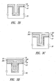
- Figures 3A- Figure 3E show the manufacturing process for one embodiment of the released beam structure according to the present invention.
- an initial trench 30 is formed in the semiconductor substrate 20, as shown in Figure 3A.
- the first conducting layer 24 and the sacrificial layer 26 are formed on the walls of the initial trench 30, as shown in Figure 3B.
- the first conducting layer 24 comprises any acceptable conductor, such as a metal layer of tungsten, titanium, tantalum, aluminum, or an additional doped polysilicon layer.
- the sacrificial layer 26 comprises an oxide layer, such as a silicon dioxide, and the thickness of such sacrificial layer 26 is around 1000-10,000 ⁇ .
- the first dielectric layer 22 could be formed between the first conducting layer 24 and the semiconductor substrate 20.
- the first dielectric layer 22 could comprise an oxide layer, such as a silicon dioxide, or comprise an oxide layer and a silicon nitride layer.
- the thickness of the first dielectric layer 22 is in the range of 200-5000 ⁇ .
- the beam 28 is deposited on the sacrificial layer 26.
- the beam 28 comprises the second conducting layer 281 and the beam material layer 282, as shown in Figure 3C.
- the beam material layer 282 comprises a doped polysilicon layer, and the thickness thereof is around 1000-6000 ⁇ .
- the beam layer 282 can be made of any acceptable material. If a heavy beam is desired, the entire beam can be made of metal or some other heavyweight material.
- the properties that can be controlled in the manufacturing of the beam include the width of the beam, the distance from the side of the trench to the beam, the length of the beam, and the weight of the beam. While in most embodiments, the beam layer 282 is a conductor, this is not required.
- the layer 281 can be contacted instead to provide the desired signal.
- the weight of the beam may be carefully controlled to be able to measure certain features.
- the beam may be made quite heavy by using pure metal or, on the other hand, it may be made lighter by using polysilicon.
- the deflection distance which can be reasonably predicted for the various materials will determine the beam length and the distances, for example, the distance between the beam and the sidewall of the trench may be different than for an all-metal beam than for a beam made fully of polysilicon or a silicon dioxide. The design of these factors can be selected based on the desired end properties of the structure.
- the second conducting layer 281 can be any acceptable conductor, such as tungsten, titanium, tantalum, aluminum, or polysilicon or a doped beam layer itself, such that the beam 28 could provide conductivity when the beam 28 contacts with the first conducting layer 24.
- the second dielectric layer 32 is formed on the beam material layer 282 to act as a protecting layer.
- the second dielectric layer 32 could comprise an oxide layer, such as a silicon dioxide, or comprise an oxide layer and a silicon nitride layer. Afterward, a portion of sacrificial layer is removed so that one end of the beam 28 remains coupled to the remaining sacrificial layer 26 and the other end of the beam 28 is movable and spaced from the walls by a selected distance.
- a mask layer 34 such as photoresist, could be first positioned on part of the second dielectric layer 32 to be retained before etching the unwanted portion of the sacrificial layer, as shown in Figure 3D. Then the unwanted portion of the beam material layer 282 and the second conducting layer 281 will be etched by any acceptable method, one of which is anisotropic etching to reveal the sacrificial layer. Thereafter, the unwanted portion of the sacrificial layer 26 will be removed through another etching process.
- the first conducting layer 24 is formed on what will become the walls of the trench, and the conductive layer 281 is around the beam 282, etch stops are automatically formed around the beam 28, and in the trench preventing unwanted over-etch conditions when manufacturing several beam structures at the same time.
- the conductive layers 24 and 281 are not etched by the same etch chemistry that etches layer 26.
- a final trench 18 will be formed after the unwanted portion of the sacrificial layer is removed, as shown in Figure 3E.
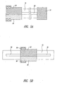
- Figure 4 is a schematic diagram of another embodiment of the present invention.
- the width and the thickness of the beam 28 could also be changed such that the beam 28 could be deflected to electrically contact with the bottom wall of the trench 18 when an acceleration force is applied in the vertical direction as shown by arrows in Figure 4.
- the beam 28 could also be deflected to electrically contact with the bottom of the trench 18 in response to a predetermined temperature variation from a first temperature to a second temperature.
- the beam structure shown in Figure 4 could be used to detect the temperature variation.
- the remaining sacrificial layer 26 could be positioned at both ends of the beam 28 as shown in Figure 5A which is another embodiment of the present invention.
- the middle part of the beam 28 could be deflected to electrically contact with the sidewalls or the bottom of the trench 18 when there is an acceleration force or temperature variation applied on such beam structure.
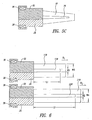
- the thickness or width of the beam 28 can be varied along its length, from a set maximum value, since the thickness or the width of the released beam is related to thickness or the width of the trench, which is a variable with a value that can be chosen during the manufacturing process.
- the width of the beam 28 varies along its length, and the width of the beam is controlled by the width of the trench 18 which also varies along its length.
- the present invention also provides a semiconductor structure comprising a plurality of beam structures having a location or shape different from each other.
- Figure 6 is a schematic diagram of another embodiment of the present invention, wherein there are a first trench 118 with a first beam 128 extending in a first direction D1 and a second trench 218 with a second beam 228 extending in a second direction D2 in this embodiment.
- the first direction D1 could be different from, or parallel to the second direction D2.
- the dimension of the first beam 128 could be different from that of the second beam 228 such that the semiconductor structure could be used to measure or detect different magnitude of the acceleration force at the direction perpendicular to the first or the second direction.
- the length L1 of the first beam 128 is different from the length L2 of the second beam 228, and the width W1 of the first beam 128 could also be different from the width W2 of the second beam 228.
- the length and width of each beam could be controlled by the length and width of different trench. Therefore, this embodiment could detect at least two different magnitudes of the acceleration forces, because different dimension beam could be deflected to electrically contact with the walls of the trench in response to different magnitude acceleration force applied to this semiconductor structure. Also, the width W3 and W4 of the trench can be selected to control the sensitivity of the detection.
- Figure 7 is a schematic diagram of another embodiment of the present invention, wherein the first direction D1 is perpendicular to the second direction D2. Therefore the first beam 128 could be deflected to contact with the walls of the first trench 118 when a predetermined acceleration force is applied in the D2 direction, and the second beam 228 could be deflected to contact with the walls of the second trench 218 when another predetermined acceleration force is applied in the D1 direction.
- the present invention it is also possible to combine different direction and different dimension of beam structures together.
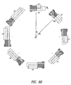
- FIG. 8A is a schematic diagram of another embodiment of the present invention, wherein there are a plurality of beam structures positioned in radial arrangement having a first common radius R1 from a first common point P1.
- Each beam structure has different length of beam varied from L1 to L8.
- each beam structure could have different width of beam by controlling the width Wt of different trench if necessary.
- each beam structure could detect different magnitude of angular acceleration because of the different dimension of each beam.
- Figure 8B is a schematic diagram of another embodiment of the present invention, wherein there are a plurality of beam structures positioned in circle arrangement having a second common radius R2 from a second common point P2.
- the length of each beam varies from L1 to L8, and of course each beam could have different width of beam by controlling the width Wt of different trench. Therefore, when the embodiment of the present invention rotates around the second common point P2, different beam structure could detect different angular velocity by measuring the acceleration force along the radial direction which is perpendicular to the direction the beam.
- Figure 9A is a schematic diagram of an integrated circuit on a semiconductor substrate according to an embodiment of the present invention.
- the integrated circuit comprises a sensor 50 and a semiconductor circuit 40.
- the sensor 50 could be the same as the beam structure shown in Figure 2A.
- the semiconductor circuit 40 on the substrate has a first node coupled to the first conducting layer through the first window 36 and a second node coupled to the beam 28 through the second window 38. Therefore, if there is an acceleration force or a temperature variation applied on the sensor 50 and the beam 28 electrically contacts with the walls of the trench 18, the semiconductor circuit 40 could detect and be in response to such electrical contact.
- Figure 9B is a schematic cross-section view of the integrated circuit along line 9B-9B in Figure 9A.
- the semiconductor circuit 40 comprises at least a MOS circuit 41, as shown in Figure 9B.
- the material of an oxide layer 411 in the MOS circuit 41 could be the same as the material of the sacrificial layer 26 in the sensor, and the material of the metal layer 412 in the MOS circuit 41 could be the same as the first conducting layer 281 of the beam 28 in the sensor 50. Therefore, the manufacturing of the sensor 50 is compatible with the existing process to manufacture MOS or CMOS circuits.
- the fabrication sequence that is used to make the trench released beam structures may also be used to simultaneously make released beam structures that are not in a trench.
- a device which is similar to the structure of the released beam device of the '209 patent is shown in Figure 10.
- the ability to simultaneously manufacture released beam structures that are in a trench and above a planar surface allows the fabrication of a released beam sensor with sensing devices that are in three orthogonal directions. Such as sensor may be used to monitor the acceleration in any direction.
- a released beam assembly 20 includes a substrate 23 and a beam 26.
- a pedestal 25 supports the structure 29 from which the beam 26 extends.
- Conductive layers on the underside of beam 26 as well as on the upper surface of substrate 23 contact each other when the beam 26 deflects under acceleration, thus providing an electrical signal which is sensed by other circuitry.
Landscapes
- Physics & Mathematics (AREA)
- Geometry (AREA)
- Engineering & Computer Science (AREA)
- Manufacturing & Machinery (AREA)
- Microelectronics & Electronic Packaging (AREA)
- Pressure Sensors (AREA)
- Micromachines (AREA)
- Measuring Temperature Or Quantity Of Heat (AREA)
- Drying Of Semiconductors (AREA)
Abstract
Description
Claims (36)
- A beam structure comprising:a semiconductor substrate;a trench extending into the semiconductor substrate, the trench having walls;a first conducting layer positioned over the walls of the trench at selected locations; anda beam positioned with the trench, the beam being connected at a first portion thereof to the substrate and being movable at a second portion thereof, the second portion being spaced from the walls of the trench by a selected distance.
- The beam structure in claim 1, further comprising a remaining sacrificial layer between the first portion of the beam and the first conducting layer.
- The beam structure in claim 2 wherein the remaining sacrificial layer comprises an oxide layer.
- The beam structure in any preceding claim wherein the beam is a cantilever beam.
- The beam structure in any preceding claim, further comprising a first dielectric layer between the trench and the first conducting layer.
- The beam structure in claim 5 wherein the first dielectric layer comprises a dual layer of a nitride layer formed on an oxide layer.
- The beam structure in any preceding claim, further comprising a second dielectric layer on the beam.
- The beam structure in any preceding claim wherein the beam comprises a second conducting layer and a beam material layer.
- The beam structure in claim 8 wherein the beam material layer comprises a doped polysilicon layer.
- The beam structure in claim 8 or 9 wherein the second conducting layer comprises a metal layer selected from the group of tungsten, titanium, tantalum, and aluminum.
- The beam structure in any preceding claim wherein the first conducting layer comprises a metal layer selected from the group of tungsten, titanium, tantalum, and aluminum.
- The beam structure in any preceding claim wherein the first conducting layer further comprises a doped polysilicon layer.
- A semiconductor structure comprising:a semiconductor substrate;a first trench extending in a first direction, the first trench having walls;a second trench extending in a second direction, the second trench having walls;a first conducting layer positioned over the walls of the first and the second trenches at selected locations;a first beam positioned with the first trench, the first beam being connected at a first portion thereof to the substrate and being movable at a second portion thereof, the second portion being spaced from the walls of the first trench by a selected distance; anda second beam positioned with the second trench, the second beam being connected at a first portion thereof to the substrate and being movable at a second portion thereof, the second portion being spaced from the walls of the second trench by a selected distance.
- The semiconductor structure in claim 13 wherein the length and/or width and/or thickness of the first beam is different from the length and/or width and/or thickness of the second beam.
- The semiconductor structure in claim 13 or 14 wherein the width of the first trench is different from the width of the second trench.
- The semiconductor structure in any of claims 13 to 15 wherein the first direction is one of parallel to and perpendicular to the second direction.
- The semiconductor structure in any of claims 13 to 16 wherein the first direction and the second direction are in an arrangement so that the first trench and the second trench have a common radius from a common point.
- The semiconductor structure in any of claims 17 wherein the first beam is perpendicular to a first line extending from the center of a circle and the second beam is perpendicular to a second line extending from the center of the same circle.
- The semiconductor structure in any of claims 17 to 18 wherein the first beam is parallel to and on a first line extending from the center of a circle and the second beam is parallel to and on a second line extending from the center of the same circle.
- The semiconductor structure in claim 13 to 19, further comprising a first dielectric layer between the first trench and the first conducting layer, and between the second trench and the first conducting layer.
- The semiconductor structure in any of claims 13 to 20, further comprising a first remaining sacrificial layer between the first portion of the first beam and the first conducting layer, and between the first portion of the second beam and the first conducting layer.
- An integrated circuit on a semiconductor substrate comprising:a sensor including:a trench extending from a first surface into the substrate, the trench having walls,a first conducting layer positioned over the walls of the trench at selected locations, anda beam positioned with the trench, the beam being connected at a first portion thereof to the substrate and being movable at a second portion thereof, the second portion being spaced from the walls by a selected distance; anda semiconductor circuit on the substrate having a first node coupled to the first conducting layer and a second node coupled to the beam layer.
- The integrated circuit in claim 22 wherein the sensor further comprises a first dielectric layer between the trench and the first conducting layer.
- The integrated circuit in claim 22 or 23 wherein the sensor further comprises a remaining sacrificial layer between the first portion of the beam and the first conducting layer.
- A method comprising:forming a trench in a semiconductor substrate;forming a first conducting layer on the walls of the trench;forming a sacrificial layer on the first conducting layer;forming a beam on the sacrificial layer; andremoving a portion of the sacrificial layer so that a first portion of the beam remains coupled to a remaining portion of the sacrificial layer and a second portion of the beam is movable and spaced from the walls by a selected distance.
- The method in claim 25 wherein the step of forming a beam comprises:forming a second conducting layer on the sacrificial layer; andforming a beam material layer on the second conducting layer.
- The method in claim 25 or 26, further comprising: forming a first dielectric layer between the trench and the first conducting layer.
- The method in any of claims 25 to 27, further comprising:forming a second dielectric layer on the beam.
- The method in any of claims 25 to 28, further comprising:applying an acceleration force to the substrate so as to deflect the beam to electrically contact with the wall of the trench.
- The method in any of claims 25 to 28, further comprising:applying a temperature variation from a first temperature to a second temperature to the substrate so as to deflect the beam to electrically contact with the wall of the trench.
- A semiconductor structure comprising:a semiconductor substrate;a first trench extending in a first direction, the first trench having walls;a second trench extending in a second direction, perpendicular to the first direction, the second trench having walls;a first conducting layer positioned over the walls of the first and the second trenches at selected locations;a first beam positioned with the first trench, the first beam being connected at a first portion thereof to the substrate and being movable at a second portion thereof, the second portion being spaced from the walls of the first trench by a selected distance;a second beam positioned with the second trench, the second beam being connected at a first portion thereof to the substrate and being movable at a second portion thereof, the second portion being spaced from the walls of the second trench by a selected distance; anda third beam that is parallel to the surface of the semiconductor substrate having its primary axis of motion perpendicular to the surface of the substrate.
- The semiconductor structure in claim 31 wherein the length and/or width and/or thickness of the first beam is the same as the length and/or width and/or thickness of the second beam.
- The semiconductor structure in claim 31 or 32 wherein the width of the first trench is the same as the width of the second trench.
- The semiconductor structure in any of claims 31 to 33 wherein the length and/or width and/or thickness of the first beam is different from the length and/or width and/or thickness of the third beam.
- The semiconductor structure in any of claims 31 to 34 wherein the third beam is built in a third trench.
- The semiconductor structure in any of claims 31 to 35 wherein the width and/or depth of the first trench is different from the width and/or depth of the third trench.
Applications Claiming Priority (2)
| Application Number | Priority Date | Filing Date | Title |
|---|---|---|---|
| US721524 | 2003-11-25 | ||
| US10/721,524 US7397097B2 (en) | 2003-11-25 | 2003-11-25 | Integrated released beam layer structure fabricated in trenches and manufacturing method thereof |
Publications (3)
| Publication Number | Publication Date |
|---|---|
| EP1547969A2 true EP1547969A2 (en) | 2005-06-29 |
| EP1547969A3 EP1547969A3 (en) | 2006-04-12 |
| EP1547969B1 EP1547969B1 (en) | 2012-10-31 |
Family
ID=34552740
Family Applications (1)
| Application Number | Title | Priority Date | Filing Date |
|---|---|---|---|
| EP04257172A Expired - Lifetime EP1547969B1 (en) | 2003-11-25 | 2004-11-19 | Integrated released beam layer structure fabricated in trenches and manufacturing method thereof |
Country Status (3)
| Country | Link |
|---|---|
| US (1) | US7397097B2 (en) |
| EP (1) | EP1547969B1 (en) |
| JP (1) | JP5043298B2 (en) |
Cited By (2)
| Publication number | Priority date | Publication date | Assignee | Title |
|---|---|---|---|---|
| WO2013049671A1 (en) * | 2011-09-28 | 2013-04-04 | DigitalOptics Corporation MEMS | Cascaded electrostatic actuator |
| US10122300B2 (en) | 2011-09-28 | 2018-11-06 | DigitalOptics Corporation MEMS | Row and column actuator control |
Families Citing this family (6)
| Publication number | Priority date | Publication date | Assignee | Title |
|---|---|---|---|---|
| JP5582001B2 (en) * | 2010-04-15 | 2014-09-03 | 大日本印刷株式会社 | Mechanical quantity sensor, combined mechanical quantity sensor, electronic circuit board and electronic device |
| JP5678535B2 (en) * | 2010-09-15 | 2015-03-04 | 大日本印刷株式会社 | Mechanical quantity sensor and method of manufacturing mechanical quantity sensor |
| CN104422548B (en) * | 2013-08-28 | 2016-12-28 | 中芯国际集成电路制造(北京)有限公司 | Capacitance pressure transducer and forming method thereof |
| JP6818297B2 (en) * | 2016-10-27 | 2021-01-20 | 国立研究開発法人産業技術総合研究所 | Cantilever structure and sensors equipped with it and manufacturing method |
| JP6818296B2 (en) * | 2016-10-27 | 2021-01-20 | 国立研究開発法人産業技術総合研究所 | Cantilever structure and sensors equipped with it and manufacturing method |
| US11279614B2 (en) | 2019-06-28 | 2022-03-22 | Analog Devices, Inc. | Low-parasitic capacitance MEMS inertial sensors and related methods |
Family Cites Families (26)
| Publication number | Priority date | Publication date | Assignee | Title |
|---|---|---|---|---|
| FR2558263B1 (en) * | 1984-01-12 | 1986-04-25 | Commissariat Energie Atomique | DIRECTIVE ACCELEROMETER AND METHOD FOR MANUFACTURING IT WITH MICROLITHOGRAPHY |
| US5016072A (en) * | 1988-01-13 | 1991-05-14 | The Charles Stark Draper Laboratory, Inc. | Semiconductor chip gyroscopic transducer |
| US4855544A (en) * | 1988-09-01 | 1989-08-08 | Honeywell Inc. | Multiple level miniature electromechanical accelerometer switch |
| JPH0644008B2 (en) * | 1990-08-17 | 1994-06-08 | アナログ・ディバイセス・インコーポレーテッド | Monolithic accelerometer |
| US5129983A (en) * | 1991-02-25 | 1992-07-14 | The Charles Stark Draper Laboratory, Inc. | Method of fabrication of large area micromechanical devices |
| US5707077A (en) * | 1991-11-18 | 1998-01-13 | Hitachi, Ltd. | Airbag system using three-dimensional acceleration sensor |
| US5198390A (en) * | 1992-01-16 | 1993-03-30 | Cornell Research Foundation, Inc. | RIE process for fabricating submicron, silicon electromechanical structures |
| US5349855A (en) * | 1992-04-07 | 1994-09-27 | The Charles Stark Draper Laboratory, Inc. | Comb drive micromechanical tuning fork gyro |
| DE69317462T2 (en) * | 1992-04-30 | 1998-08-27 | Texas Instruments Inc | Digital accelerometer |
| JPH05340959A (en) * | 1992-06-08 | 1993-12-24 | Nissan Motor Co Ltd | Fabrication of semiconductor acceleration sensor |
| EP0683921B1 (en) * | 1993-02-04 | 2004-06-16 | Cornell Research Foundation, Inc. | Microstructures and single mask, single-crystal process for fabrication thereof |
| JP3303430B2 (en) * | 1993-05-21 | 2002-07-22 | 株式会社デンソー | FET type acceleration sensor |
| US5610335A (en) * | 1993-05-26 | 1997-03-11 | Cornell Research Foundation | Microelectromechanical lateral accelerometer |
| JPH07209327A (en) * | 1994-01-18 | 1995-08-11 | Murata Mfg Co Ltd | Acceleration sensor |
| US6316796B1 (en) * | 1995-05-24 | 2001-11-13 | Lucas Novasensor | Single crystal silicon sensor with high aspect ratio and curvilinear structures |
| DE19610782B4 (en) * | 1996-03-19 | 2004-08-12 | Robert Bosch Gmbh | Process for the production of micromechanical structures |
| DE69838709T2 (en) | 1997-09-10 | 2008-10-30 | Matsushita Electric Industrial Co., Ltd., Kadoma | METHOD FOR PRODUCING AN ACCELERATOR |
| US6058778A (en) | 1997-10-24 | 2000-05-09 | Stmicroelectronics, Inc. | Integrated sensor having plurality of released beams for sensing acceleration |
| US5917226A (en) | 1997-10-24 | 1999-06-29 | Stmicroelectronics, Inc. | Integrated released beam, thermo-mechanical sensor for sensing temperature variations and associated methods |
| US6028343A (en) | 1997-10-24 | 2000-02-22 | Stmicroelectronics, Inc. | Integrated released beam sensor for sensing acceleration and associated methods |
| US6124765A (en) | 1997-10-24 | 2000-09-26 | Stmicroelectronics, Inc. | Integrated released beam oscillator and associated methods |
| US6180536B1 (en) * | 1998-06-04 | 2001-01-30 | Cornell Research Foundation, Inc. | Suspended moving channels and channel actuators for microfluidic applications and method for making |
| US6389899B1 (en) * | 1998-06-09 | 2002-05-21 | The Board Of Trustees Of The Leland Stanford Junior University | In-plane micromachined accelerometer and bridge circuit having same |
| US6211598B1 (en) * | 1999-09-13 | 2001-04-03 | Jds Uniphase Inc. | In-plane MEMS thermal actuator and associated fabrication methods |
| IL139730A0 (en) | 2000-11-16 | 2002-02-10 | Micma Engineering Ltd | Silicon capacitive accelerometer |
| JP4216525B2 (en) * | 2002-05-13 | 2009-01-28 | 株式会社ワコー | Acceleration sensor and manufacturing method thereof |
-
2003
- 2003-11-25 US US10/721,524 patent/US7397097B2/en not_active Expired - Lifetime
-
2004
- 2004-11-19 EP EP04257172A patent/EP1547969B1/en not_active Expired - Lifetime
- 2004-11-25 JP JP2004340417A patent/JP5043298B2/en not_active Expired - Lifetime
Cited By (3)
| Publication number | Priority date | Publication date | Assignee | Title |
|---|---|---|---|---|
| WO2013049671A1 (en) * | 2011-09-28 | 2013-04-04 | DigitalOptics Corporation MEMS | Cascaded electrostatic actuator |
| US9350271B2 (en) | 2011-09-28 | 2016-05-24 | DigitalOptics Corporation MEMS | Cascaded electrostatic actuator |
| US10122300B2 (en) | 2011-09-28 | 2018-11-06 | DigitalOptics Corporation MEMS | Row and column actuator control |
Also Published As
| Publication number | Publication date |
|---|---|
| JP2005169616A (en) | 2005-06-30 |
| JP5043298B2 (en) | 2012-10-10 |
| US20050110110A1 (en) | 2005-05-26 |
| EP1547969B1 (en) | 2012-10-31 |
| EP1547969A3 (en) | 2006-04-12 |
| US7397097B2 (en) | 2008-07-08 |
Similar Documents
| Publication | Publication Date | Title |
|---|---|---|
| US6000287A (en) | Capacitor center of area sensitivity in angular motion micro-electromechanical systems | |
| US8227876B2 (en) | Single crystal silicon sensor with additional layer and method of producing the same | |
| US6105428A (en) | Sensor and method of use | |
| US6149190A (en) | Micromechanical accelerometer for automotive applications | |
| EP3912953B1 (en) | Process for manufacturing a micro-electro-mechanical device, in particular a movement sensor with capacitive control/detection, and mems device | |
| US6170332B1 (en) | Micromechanical accelerometer for automotive applications | |
| US6065341A (en) | Semiconductor physical quantity sensor with stopper portion | |
| US8096182B2 (en) | Capacitive sensor with stress relief that compensates for package stress | |
| US5563343A (en) | Microelectromechanical lateral accelerometer | |
| EP0702796B1 (en) | Microelectromechanical lateral accelerometer | |
| US6792804B2 (en) | Sensor for measuring out-of-plane acceleration | |
| JP4214565B2 (en) | Manufacturing method of semiconductor dynamic quantity sensor | |
| US7270003B2 (en) | BMEMS-type high-sensitivity inertial sensor and manufacturing process thereof | |
| US5181156A (en) | Micromachined capacitor structure and method for making | |
| US20060070441A1 (en) | Micro-electro-mechanical structure having electrically insulated regions and manufacturing process thereof | |
| US7397097B2 (en) | Integrated released beam layer structure fabricated in trenches and manufacturing method thereof | |
| US6215645B1 (en) | Differential capacitor structure | |
| US5583291A (en) | Micromechanical anchor structure | |
| JP2011112620A (en) | Acceleration sensor | |
| EP1676809B1 (en) | Weighted released-beam sensor | |
| US7179674B2 (en) | Bi-directional released-beam sensor | |
| US5824565A (en) | Method of fabricating a sensor | |
| EP0877255A1 (en) | Micromechanical Accelerometer for Automotive Applications | |
| JP5355028B2 (en) | Acceleration sensor | |
| US12415718B2 (en) | Impact-resistant micromechanical arms |
Legal Events
| Date | Code | Title | Description |
|---|---|---|---|
| PUAI | Public reference made under article 153(3) epc to a published international application that has entered the european phase |
Free format text: ORIGINAL CODE: 0009012 |
|
| AK | Designated contracting states |
Kind code of ref document: A2 Designated state(s): AT BE BG CH CY CZ DE DK EE ES FI FR GB GR HU IE IS IT LI LU MC NL PL PT RO SE SI SK TR |
|
| AX | Request for extension of the european patent |
Extension state: AL HR LT LV MK YU |
|
| PUAL | Search report despatched |
Free format text: ORIGINAL CODE: 0009013 |
|
| AK | Designated contracting states |
Kind code of ref document: A3 Designated state(s): AT BE BG CH CY CZ DE DK EE ES FI FR GB GR HU IE IS IT LI LU MC NL PL PT RO SE SI SK TR |
|
| AX | Request for extension of the european patent |
Extension state: AL HR LT LV MK YU |
|
| 17P | Request for examination filed |
Effective date: 20061005 |
|
| 17Q | First examination report despatched |
Effective date: 20061106 |
|
| AKX | Designation fees paid |
Designated state(s): DE FR GB IT |
|
| REG | Reference to a national code |
Ref country code: DE Ref legal event code: R079 Ref document number: 602004039849 Country of ref document: DE Free format text: PREVIOUS MAIN CLASS: B81B0003000000 Ipc: B81C0001000000 |
|
| RIC1 | Information provided on ipc code assigned before grant |
Ipc: B81C 1/00 20060101AFI20120208BHEP |
|
| GRAP | Despatch of communication of intention to grant a patent |
Free format text: ORIGINAL CODE: EPIDOSNIGR1 |
|
| GRAS | Grant fee paid |
Free format text: ORIGINAL CODE: EPIDOSNIGR3 |
|
| GRAA | (expected) grant |
Free format text: ORIGINAL CODE: 0009210 |
|
| AK | Designated contracting states |
Kind code of ref document: B1 Designated state(s): DE FR GB IT |
|
| REG | Reference to a national code |
Ref country code: GB Ref legal event code: FG4D |
|
| REG | Reference to a national code |
Ref country code: DE Ref legal event code: R096 Ref document number: 602004039849 Country of ref document: DE Effective date: 20121227 |
|
| PG25 | Lapsed in a contracting state [announced via postgrant information from national office to epo] |
Ref country code: IT Free format text: LAPSE BECAUSE OF FAILURE TO SUBMIT A TRANSLATION OF THE DESCRIPTION OR TO PAY THE FEE WITHIN THE PRESCRIBED TIME-LIMIT Effective date: 20121031 |
|
| PLBE | No opposition filed within time limit |
Free format text: ORIGINAL CODE: 0009261 |
|
| STAA | Information on the status of an ep patent application or granted ep patent |
Free format text: STATUS: NO OPPOSITION FILED WITHIN TIME LIMIT |
|
| GBPC | Gb: european patent ceased through non-payment of renewal fee |
Effective date: 20130131 |
|
| 26N | No opposition filed |
Effective date: 20130801 |
|
| REG | Reference to a national code |
Ref country code: DE Ref legal event code: R097 Ref document number: 602004039849 Country of ref document: DE Effective date: 20130801 |
|
| PG25 | Lapsed in a contracting state [announced via postgrant information from national office to epo] |
Ref country code: GB Free format text: LAPSE BECAUSE OF NON-PAYMENT OF DUE FEES Effective date: 20130131 |
|
| REG | Reference to a national code |
Ref country code: FR Ref legal event code: PLFP Year of fee payment: 12 |
|
| REG | Reference to a national code |
Ref country code: FR Ref legal event code: PLFP Year of fee payment: 13 |
|
| REG | Reference to a national code |
Ref country code: FR Ref legal event code: PLFP Year of fee payment: 14 |
|
| REG | Reference to a national code |
Ref country code: FR Ref legal event code: PLFP Year of fee payment: 15 |
|
| REG | Reference to a national code |
Ref country code: DE Ref legal event code: R082 Ref document number: 602004039849 Country of ref document: DE Representative=s name: PAGE, WHITE & FARRER GERMANY LLP, DE |
|
| PGFP | Annual fee paid to national office [announced via postgrant information from national office to epo] |
Ref country code: FR Payment date: 20191022 Year of fee payment: 16 |
|
| PG25 | Lapsed in a contracting state [announced via postgrant information from national office to epo] |
Ref country code: FR Free format text: LAPSE BECAUSE OF NON-PAYMENT OF DUE FEES Effective date: 20201130 |
|
| PGFP | Annual fee paid to national office [announced via postgrant information from national office to epo] |
Ref country code: DE Payment date: 20231019 Year of fee payment: 20 |
|
| REG | Reference to a national code |
Ref country code: DE Ref legal event code: R071 Ref document number: 602004039849 Country of ref document: DE |