EP1547192B1 - Device for transmitting or emitting high-frequency waves - Google Patents
Device for transmitting or emitting high-frequency waves Download PDFInfo
- Publication number
- EP1547192B1 EP1547192B1 EP03798044A EP03798044A EP1547192B1 EP 1547192 B1 EP1547192 B1 EP 1547192B1 EP 03798044 A EP03798044 A EP 03798044A EP 03798044 A EP03798044 A EP 03798044A EP 1547192 B1 EP1547192 B1 EP 1547192B1
- Authority
- EP
- European Patent Office
- Prior art keywords
- coupling
- coupling opening
- ground plane
- frequency
- substrate
- Prior art date
- Legal status (The legal status is an assumption and is not a legal conclusion. Google has not performed a legal analysis and makes no representation as to the accuracy of the status listed.)
- Expired - Lifetime
Links
- 230000008878 coupling Effects 0.000 claims description 87
- 238000010168 coupling process Methods 0.000 claims description 87
- 238000005859 coupling reaction Methods 0.000 claims description 87
- 239000000758 substrate Substances 0.000 claims description 38
- 239000000919 ceramic Substances 0.000 claims description 7
- 230000005540 biological transmission Effects 0.000 claims description 6
- 230000005284 excitation Effects 0.000 claims description 4
- 229910010293 ceramic material Inorganic materials 0.000 claims description 2
- 238000000926 separation method Methods 0.000 claims description 2
- 238000011161 development Methods 0.000 description 11
- 230000018109 developmental process Effects 0.000 description 11
- 230000008901 benefit Effects 0.000 description 10
- 239000010410 layer Substances 0.000 description 7
- 239000000463 material Substances 0.000 description 7
- 230000000694 effects Effects 0.000 description 4
- 230000005855 radiation Effects 0.000 description 4
- 238000002955 isolation Methods 0.000 description 3
- 230000002411 adverse Effects 0.000 description 2
- 230000007423 decrease Effects 0.000 description 2
- 230000006735 deficit Effects 0.000 description 2
- 230000005684 electric field Effects 0.000 description 2
- 230000006872 improvement Effects 0.000 description 2
- 238000004519 manufacturing process Methods 0.000 description 2
- 230000010355 oscillation Effects 0.000 description 2
- 238000004088 simulation Methods 0.000 description 2
- 230000001629 suppression Effects 0.000 description 2
- 230000009471 action Effects 0.000 description 1
- 230000006978 adaptation Effects 0.000 description 1
- 230000008859 change Effects 0.000 description 1
- 239000004020 conductor Substances 0.000 description 1
- 230000001419 dependent effect Effects 0.000 description 1
- 238000010586 diagram Methods 0.000 description 1
- 230000005672 electromagnetic field Effects 0.000 description 1
- 238000005516 engineering process Methods 0.000 description 1
- 230000001771 impaired effect Effects 0.000 description 1
- 239000002184 metal Substances 0.000 description 1
- 230000003071 parasitic effect Effects 0.000 description 1
- 230000035515 penetration Effects 0.000 description 1
- 230000002093 peripheral effect Effects 0.000 description 1
- 230000002787 reinforcement Effects 0.000 description 1
- 230000008054 signal transmission Effects 0.000 description 1
- 239000002356 single layer Substances 0.000 description 1
- 230000000638 stimulation Effects 0.000 description 1
- 230000007704 transition Effects 0.000 description 1
Images


Classifications
-
- H—ELECTRICITY
- H01—ELECTRIC ELEMENTS
- H01Q—ANTENNAS, i.e. RADIO AERIALS
- H01Q9/00—Electrically-short antennas having dimensions not more than twice the operating wavelength and consisting of conductive active radiating elements
- H01Q9/04—Resonant antennas
- H01Q9/0407—Substantially flat resonant element parallel to ground plane, e.g. patch antenna
- H01Q9/045—Substantially flat resonant element parallel to ground plane, e.g. patch antenna with particular feeding means
-
- H—ELECTRICITY
- H01—ELECTRIC ELEMENTS
- H01Q—ANTENNAS, i.e. RADIO AERIALS
- H01Q13/00—Waveguide horns or mouths; Slot antennas; Leaky-waveguide antennas; Equivalent structures causing radiation along the transmission path of a guided wave
- H01Q13/08—Radiating ends of two-conductor microwave transmission lines, e.g. of coaxial lines, of microstrip lines
-
- H—ELECTRICITY
- H01—ELECTRIC ELEMENTS
- H01Q—ANTENNAS, i.e. RADIO AERIALS
- H01Q9/00—Electrically-short antennas having dimensions not more than twice the operating wavelength and consisting of conductive active radiating elements
- H01Q9/04—Resonant antennas
- H01Q9/0407—Substantially flat resonant element parallel to ground plane, e.g. patch antenna
- H01Q9/045—Substantially flat resonant element parallel to ground plane, e.g. patch antenna with particular feeding means
- H01Q9/0457—Substantially flat resonant element parallel to ground plane, e.g. patch antenna with particular feeding means electromagnetically coupled to the feed line
Description
Die vorliegende Erfindung betrifft eine Vorrichtung zum Übertragen bzw. Abstrahlen hochfrequenter Wellen gemäß dem Oberbegriff des Anspruchs 1, wie aus
Eine ebensolche Vorrichtung ist aus der
Aus der
Die
Vorrichtungen zum Abstrahlen elektromagnetischer Wellen, wie beispielsweise planare Antennenelemente, die über einen Schlitz zur Schwingung und damit zur Abstrahlung hochfrequenter Wellen angeregt werden, sind beispielsweise in der Richtfunk-, Satellitenfunk- oder Radartechnik weit verbreitet. Vorzugsweise finden sie im Mikrowellenbereich Anwendung, da hier kleine Baugrößen und damit einfache Realisierungen unter Einsatz geringer Kosten möglich sind.Devices for emitting electromagnetic waves, such as planar antenna elements, which are excited via a slot for oscillation and thus for the emission of high-frequency waves, are widely used, for example, in radio relay, satellite radio or radar technology. They are preferably used in the microwave range, since small sizes and therefore simple implementations using low costs are possible here.
Eine übliche planare Antenneneinrichtung ist mit Bezug auf
Von Nachteil bei dieser Anordnung ist, dass Mikrostreifenleitungssubstrate 11 bei höheren Frequenzen sehr dünn werden, z.B. 254 µm bei einer short range radar-Anwendung (SRR) bei 24GHz, und keine ausreichende Strukturfestigkeit für eine Verbauung aufweisen. Deshalb müssen diese Substrate 11 mit einem starren Trägermaterial 18, wie in
Eine weitere herkömmliche Ausführungsform einer schlitzgekoppelten Antenne verwendet zur Speisung des Einzelstrahlers 16 eine sogenannte "vergrabene", signalführende Leitung 10 mit abrupten Leitungsende 10', die in Form von einer sogenannten Triplate-Leitung ausgeführt ist und ihrerseits ebenfalls über einen Schlitz 14 den Einzelstrahler 16 zur Abstrahlung anregt. Die Signalleitung 10 ist im wesentlichen planparallel zwischen zwei Masseflächen 12, 13 angeordnet, wobei im gemäß
Darüber hinaus beeinflusst ein vergrabenes Speisenetzwerk die Abstrahlcharakteristik einer solchen Anordnung nicht negativ, im Gegensatz zu, insbesondere bei höheren Frequenzen, "offenen" Verteiler- bzw. Speisenetzwerken, welche erheblich zu parasitärer Abstrahlung beitragen. Von Vorteil ist außerdem die Möglichkeit einfach herzustellenden Multischicht- bzw. Multilayer-Anordnungen vorzusehen, da deren Einzelschichten bzw. Einzellayer gute Hochfrequenzeigenschaften aufweisen und die jeweiligen zu vergrabenden Leitungsstrukturen tragen. Bei Verwendung geeigneter Layer- bzw. Substratmaterialien, wie beispielsweise Keramiken, kann auf die Verbindung mit einem zusätzlichen mechanischen Träger verzichtet werden, da die Multilayer-Anordnung über eine ausreichende Strukturstabilität verfügt. Insbesondere low temperature cofired ceramic (LTCC)-Substrate sind auf diesem Gebiet geeignet.In addition, a buried feed network does not adversely affect the radiation characteristics of such an arrangement, in contrast to, especially at higher frequencies, "open" distribution or feed networks, which contribute significantly to parasitic radiation. Another advantage is the possibility to provide easily produced multi-layer or multilayer arrangements, since their individual layers or single layers have good high-frequency properties and carry the respective to be buried line structures. When using suitable layer or substrate materials, such as ceramics, can be dispensed with the connection with an additional mechanical support, since the multilayer arrangement on has sufficient structural stability. In particular, low temperature cofired ceramic (LTCC) substrates are suitable in this field.
Die eben mit Bezug auf
Generell gilt der Zusammenhang, dass die Grenzfrequenz fg eines Hohlleitermodes zu niedrigeren Frequenzen verschoben wird, wenn der Abstand der elektrisch leitenden, beispielsweise metallischen Wände vergrößert wird. Dabei erhöht sich zugleich die Anzahl der in einem bestimmten Frequenzband ausbreitungsfähigen Moden stetig. Werden nun im Substrat 11 solche Moden durch leerlaufende Leitungsenden angeregt, so wird einerseits die über das Strahlerelement 16 abgestrahlte Leistung reduziert und andererseits Verkopplungen mit anderen Schaltungsteilen innerhalb des Substrats 11, z.B. weiteren Antennenelementen, begünstigt, welche sich nachteilig auf die Antennencharakteristik und das gesamte Systemverhalten auswirken.In general, the relationship applies that the cut-off frequency f g of a waveguide mode is shifted to lower frequencies when the distance between the electrically conductive, for example, metallic walls is increased. At the same time, the number of modes capable of propagation in a certain frequency band increases steadily. If such modes are excited in the
Die erfindungsgemäße Vorrichtung zum Übertragen bzw. Abstrahlen hochfrequenter Wellen mit den Merkmalen des Anspruchs 1 weist gegenüber dem bekannten Lösungsansatz den Vorteil auf, dass die Anregung von Substrat oder Hohlleitermoden in einer schlitzgekoppelten Antennenanordnung mit symmetrischer oder unsymmetrischer Triplate-Leitung verhindert bzw. auf ein für das Verhalten der Antenne bzw. des Systems nicht mehr relevantes Maß reduziert wird, ohne die grundsätzliche Wirkungsweise einer schlitzgekoppelten Abstrahlvorrichtung negativ zu beeinflussen.The device according to the invention for transmitting or emitting high-frequency waves with the features of
Die erfindungsgemäße Vorrichtung ermöglicht, eine kostengünstige Verbesserung der Funktion der Antenne bereitzustellen, da die Unterdrückung der beschriebenen Anregung von Substrat- oder Hohlleitermoden zur Verbesserung der Effizienz der Antenne und damit zur Verbesserung des Systemverhaltens beiträgt.The device according to the invention makes it possible to provide a cost-effective improvement in the function of the antenna, since the suppression of the described excitation of substrate or waveguide modes contributes to improving the efficiency of the antenna and thus to improving the system behavior.
Die der vorliegenden Erfindung zugrunde liegende Idee besteht im wesentlichen darin, eine Abschirmungsmaßnahme sowohl im Bereich der Signalleitung als auch im Bereich des Koppelschlitzes vorzusehen und in ihrer Dimensionierung an beide Anforderungen anzupassen.The idea underlying the present invention essentially consists in providing a shielding measure both in the area of the signal line and in the area of the coupling slot and adapting their dimensioning to both requirements.
Mit anderen Worten wird eine Vorrichtung zum Übertragen bzw. Abstrahlen hochfrequenter Wellen vorgesehen, welche eine mit einem Ende versehene Mikrostreifenleitung in einem Substrat zum Übertragen hochfrequenter Nutzsignale aufweist, eine erste Massefläche und eine zweite Massefläche, welche auf entgegenliegenden Seiten der Mikrostreifenleitung vorgesehen sind, zum Abschirmen der Mikrostreifenleitung bereitstellt, eine Öffnung in der ersten Massefläche in einem vorbestimmten Abstand zum Ende der Streifenleitung zum Auskoppeln eines hochfrequenten Signals vorsieht, eine Durchkontaktierungseinrichtung zum leitfähigen Verbinden der ersten Massefläche mit der zweiten Massefläche in der Peripherie der Mikrostreifenleitung zum Abschirmen derselben aufweist (z.B. durch sogenannte Vias) und eine planare Kopplungseinrichtung zum Aufnehmen und Übertragen des hochfrequenten Nutzsignals bereitstellt, wobei die Durchkontaktierungseinrichtung derart strukturiert und/oder dimensioniert ist, dass bei gegebener Frequenz des Nutzsignals im wesentlichen keine ausbreitungsfähigen bzw. resonanzfähigen Hohlleitermoden im Substrat auftreten.In other words, an apparatus for transmitting high-frequency waves is provided, which has an end-provided microstrip line in a substrate for transmitting high-frequency useful signals, a first ground plane and a second ground plane, which are provided on opposite sides of the microstrip line, for shielding the microstrip line, providing an opening in the first ground plane at a predetermined distance from the end of the strip line for coupling out a high frequency signal, via means for electrically connecting the first ground plane to the second ground plane in the first ground plane Peripheral the microstrip line for shielding the same has (eg by so-called vias) and provides a planar coupling device for receiving and transmitting the high-frequency useful signal, wherein the via device is structured and / or dimensioned such that at a given frequency of the useful signal substantially no propagatable or resonant capable Waveguide modes occur in the substrate.
In den Unteransprüchen finden sich vorteilhafte Weiterbildungen und Verbesserungen der in Anspruch 1 angegebenen Vorrichtung.In the dependent claims are advantageous developments and improvements of the device specified in
Erfindungsgemäß weitet sich die Struktur der Durchkontaktierungseinrichtung im Bereich der Kopplungsöffnung auf. Dies erbringt den Vorteil, dass die Ankopplung an ein Abstrahlelement (Patch) durch die abschirmende Durchkontaktierungseinrichtung im Bereich der Kopplungsöffnung nicht behindert wird.According to the invention, the structure of the plated-through device widens in the region of the coupling opening. This provides the advantage that the coupling to a radiating element (patch) is not hindered by the shielding through-connection device in the region of the coupling opening.
Erfindungsgemäß ist ein Abstand a zwischen gegenüberliegenden Durchkontaktierungseinrichtungen im Bereich der Mikrostreifenleitung kleiner als der Quotient aus ![]()
![]()
Gemäß einer weiteren bevorzugten Weiterbildung besteht zwischen der Breite B zwischen gegenüberliegenden Durchkontaktierungseinrichtungen im Bereich der Kopplungsöffnung und der Länge L der Durchkontaktierungseinrichtung im Bereich der Kopplungsöffnung folgender Zusammenhang 
wobei C0 für die Lichtgeschwindigekeit im Vakuum, εr für die dielektrische Permittivität des Substrats und fres für eine Resonanzfrequenz eines anregbaren Hohlleitermodes steht, welche oberhalb eines Nutzsignalfrequenzbandes vorzusehen ist. Dies ist ein Vorteil für die Dimensionierung der Durchkontaktierungs- bzw. Via-Wände im Bereich des Koppelschlitzes, da auf diese Weise vermieden wird, dass unerwünschte Resonanzfrequenzen Hohlraumresonanzen innerhalb der Schirmwände im Bereich des Koppelschlitzes bilden.According to a further preferred development, the following relationship exists between the width B between opposing via-contacting devices in the region of the coupling opening and the length L of the through-connection device in the region of the coupling opening
where C 0 stands for the speed of light in vacuum, ε r for the dielectric permittivity of the substrate and f res for a resonant frequency of a stimulable waveguide mode, which is to be provided above a useful signal frequency band. This is an advantage for the dimensioning of the via or via walls in the region of the coupling slot, since in this way it is avoided that undesired resonance frequencies form cavity resonances within the screen walls in the region of the coupling slot.
Gemäß einer weiteren bevorzugten Weiterbildung weist die Resonanzfrequenz einen größeren Abstand als etwa einige Prozent oberhalb vom Nutzsignalfrequenzband auf. Auf diese Weise wird eine sichere Vermeidung von Resonanzerscheinungen gewährleistet.According to a further preferred development, the resonance frequency has a greater distance than about a few percent above the useful signal frequency band. In this way, a safe avoidance of resonance phenomena is ensured.
Gemäß einer weiteren bevorzugten Weiterbildung ist die Vorrichtung für Nutzsignale in einem Frequenzband zwischen 20 GHz und 30 GHz dimensioniert. So ist die Vorrichtung beispielsweise für den Einsatz in einem SRR(short range radar)-Anwendungsfall geeignet.According to a further preferred development, the device is dimensioned for useful signals in a frequency band between 20 GHz and 30 GHz. For example, the device is suitable for use in an SRR (short range radar) application.
Gemäß einer weiteren bevorzugten Weiterbildung besteht die Durchkontaktierungseinrichtung aus diskreten Durchkontaktierungselementen, welche lateral benachbart zueinander, vorzugsweise eine elektromagnetisch abschirmende Wand bildend, angeordnet sind. Dies birgt den Vorteil einer guten Abschirmung bei kostengünstig herzustellenden Durchkontaktierungselementen, wobei sich die Wahl des Abstandes nach der Frequenz richtet.According to a further preferred development, the plated-through device consists of discrete through-connection elements, which are arranged laterally adjacent to one another, preferably forming an electromagnetic-shielding wall. This has the advantage of good shielding at cost-to-produce via elements, with the choice of the distance depends on the frequency.
Gemäß einer weiteren bevorzugten Weiterbildung sind die diskreten Durchkontaktierungselemente rund und/oder zylinderförmig gebildet. Eine einfache Herstellung kann dadurch gewährleistet werden.According to a further preferred development, the discrete feedthrough elements are formed round and / or cylindrical. A simple production can be ensured.
Gemäß einer weiteren bevorzugten Weiterbildung bildet die Durchkontaktierungseinrichtung eine durchgängige Wand. Dies bietet den Vorteil einer geschlossenen Abschirmeinrichtung, beispielsweise in Form einer metallischen Schicht, welche nahezu keinerlei elektromagnetische Ein- bzw. Auskopplungen zulässt.According to a further preferred development, the through-connection device forms a continuous wall. This offers the advantage of a closed shielding device, for example in the form of a metallic layer, which allows almost no electromagnetic input or output couplings.
Gemäß einer weiteren bevorzugten Weiterbildung ist im Bereich longitudinal benachbart des Endes der Streifenleitung die Durchkontaktierungseinrichtung durchgängig vorgesehen.According to a further preferred development, the through-connection device is provided continuously in the region longitudinally adjacent to the end of the strip line.
Von Vorteil ist dabei eine vollständige Abschirmung der Streifenleitung.The advantage here is a complete shielding of the stripline.
Gemäß einer weiteren bevorzugten Weiterbildung ist im Bereich longitudinal benachbart des Endes der Streifenleitung die Durchkontaktierungseinrichtung mit einer Lücke versehen. Dadurch wird bei leicht vermindertem Herstellungsaufwand kaum elektromagnetische Abstrahlung abgegeben bzw. aufgenommen.According to a further preferred development, the through-connection device is provided with a gap in the region longitudinally adjacent to the end of the strip line. As a result, little electromagnetic emission is emitted or absorbed at a slightly reduced production cost.
Gemäß einer weiteren bevorzugten Weiterbildung ist die Mikrostreifenleitung näher an der mit der Kopplungsöffnung versehenen Massefläche als an der anderen Massefläche im Substrat angeordnet oder umgekehrt. Dies birgt den Vorteil einer unsymmetrischen Struktur, welche z.B. bei Ankopplung einer weiteren Mikrostreifenleitung über die Kopplungsöffnung vonnöten ist.According to a further preferred refinement, the microstrip line is arranged closer to the ground area provided with the coupling opening than to the other ground area in the substrate or vice versa. This has the advantage of an asymmetric structure, which e.g. when coupling another microstrip line via the coupling opening is needed.
Erfindungsgemäß ist die Mikrostreifenleitung in etwa äquidistant zwischen der mit der Kopplungsöffnung versehenen Massefläche und der anderen Massefläche im Substrat angeordnet. Dies stellt den Vorteil einer einfachen Anordnung bereit.According to the invention, the microstrip line is arranged approximately equidistantly between the ground plane provided with the coupling opening and the other ground plane in the substrate. This provides the advantage of a simple arrangement.
Gemäß einer weiteren bevorzugten Weiterbildung bildet die planare Kopplungseinrichtung eine zweite Mikrostreifenleitung in einer anderen Ebene, welche unter galvanischer Trennung zur elektromagnetischen Ankopplung dieser weiteren Mikrostreifenleitung vorgesehen ist. Auf diese Weise wird eine Signalübertragungseinrichtung unter galvanischer Trennung vorteilhaft bereitgestellt.According to a further preferred development, the planar coupling device forms a second microstrip line in another plane, which is provided with galvanic isolation for the electromagnetic coupling of this further microstrip line. In this way, a signal transmission device is advantageously provided with galvanic isolation.
Gemäß einer weiteren bevorzugten Weiterbildung sind beide Mikrostreifenleitungen im wesentlichen gleichartig ausgebildet und überlappen sich in longitudinaler Richtung um einen zweifachen vorbestimmten Abstand, welcher vorzugsweise in etwa der halben Wellenlänge des koppelnden Nutzsignals entspricht. Somit wird eine maximale elektromagnetische Kopplung zwischen den zwei Mikrostreifenleitungen sichergestellt.According to a further preferred embodiment, both microstrip lines are formed substantially the same and overlap in the longitudinal direction by a two-fold predetermined distance, which preferably corresponds approximately to half the wavelength of the coupling useful signal. Thus, maximum electromagnetic coupling between the two microstrip lines is ensured.
Gemäß einer weiteren bevorzugten Weiterbildung ist die Kopplungsöffnung parallel der Masseflächen schlitzförmig und/oder rechteckförmig vorgesehen. Dies ermöglicht ein einfaches kostengünstig herzustellendes Kopplungsöffnungs-Layout in der Massefläche und bietet eine gute Aus- bzw. Einkopplung durch den Schlitz.According to a further preferred development, the coupling opening is provided in parallel with the ground surfaces in slot-shaped and / or rectangular fashion. This allows a simple cost-effective-to-produce coupling-hole layout in the ground plane and provides good coupling through the slot.
Ausführungsbeispiele der Erfindung sind in den Zeichnungen dargestellt und in der nachfolgenden Beschreibung näher erläutert.Embodiments of the invention are illustrated in the drawings and explained in more detail in the following description.
- Fig. 1Fig. 1
- eine Schrägansicht eines Ausschnitts zur Erläuterung einer ersten Ausführungsform der vorliegenden Erfindung;an oblique view of a section for explaining a first embodiment of the present invention;
- Fig. 2Fig. 2
- eine Schrägansicht zur Erläuterung der ersten Ausführungsform der vorliegenden Erfindung;an oblique view for explaining the first embodiment of the present invention;
- Fig. 3Fig. 3
- eine Draufsicht einer schematischen Abstrahlvorrichtung zur Erläuterung einer zweiten Ausführungsform der vorliegenden Erfindung;a plan view of a schematic emitting device for explaining a second embodiment of the present invention;
- Fig. 4Fig. 4
-
ein Simulationsschaubild zur Erläuterung der Funktionsweise der mit Bezug auf
Fig. 3 erläuterten Abstrahlvorrichtung;a simulation diagram for explaining the operation of with reference toFig. 3 explained emitting device; - Fig. 5A,BFig. 5A, B
-
eine schematische Darstellung einer galvanisch getrennten Kopplungseinrichtung zur Erläuterung einer dritten Ausführungsform der vorliegenden Erfindung, wobei
Fig. 5A einen Längsschnitt undFig. 5B einen Querschnitt entlang der Schnittebene A verdeutlicht;a schematic representation of a galvanically isolated coupling device for explaining a third embodiment of the present invention, whereinFig. 5A a longitudinal section andFig. 5B a cross section along the sectional plane A illustrates; - Fig. 6A,BFig. 6A, B
-
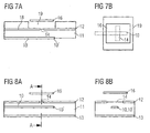
eine schematische Darstellung eines üblichen schlitzgekoppelten Planarstrahlers, wobei
Fig. 6A einen Längsschnitt undFig. 6B eine Draufsicht verdeutlicht;a schematic representation of a conventional slit-coupled Planarstrahlers, whereinFig. 6A a longitudinal section andFig. 6B a plan view illustrates; - Fig. 7A,BFig. 7A, B
-
eine schematische Darstellung der mit Bezug auf
Fig. 6A , B dargestellten Anordnung mit einer zusätzlichen mechanischen Verstärkung, wobeiFig. 7A einen Längsschnitt undFig. 7B eine Draufsicht verdeutlicht; unda schematic representation of with reference toFig. 6A , B illustrated arrangement with an additional mechanical reinforcement, whereinFig. 7A a longitudinal section andFig. 7B a plan view illustrates; and - Fig. 8A,BFig. 8A, B
-
eine schematische Darstellung eines üblichen schlitzgekoppelten Planarstrahlers mit einer unsymmetrischen Triplate-Leitungsspeisung, wobei
Fig. 8A einen Längsschnitt undFig. 8B einen Querschnitt entlang der Schnittebene A verdeutlicht.a schematic representation of a conventional slot-coupled Planarstrahlers with a single-ended tripple-line supply, whereinFig. 8A a longitudinal section andFig. 8B a cross section along the sectional plane A illustrates.
In den Figuren bezeichnen gleiche Bezugszeichen gleiche oder funktionsgleiche Bestandteile.In the figures, the same reference numerals designate the same or functionally identical components.
In
Der untere Abschluss der dargestellten Anordnung wird von einer zweiten Massefläche 13 gebildet, welche wie die erste Massefläche aus einem elektrisch leitfähigen Material, vorzugsweise ein Metall aufweisend, besteht. Die erste Massefläche 12 verfügt über eine Kopplungsöffnung 14, welche vorzugsweise rechteckig und/oder schlitzförmig vorgesehen ist, und welche mit Bezug auf ein abruptes Ende 10' der Mikrostreifenleitung 10 einen vorbestimmten Abstand d (nicht dargestellt) aufweist. Diese Kopplungsöffnung 14 ist in Y-Richtung mittig zu der Streifenleitung 10 bzw. dem Ende der Streifenleitung 10' und im rechten Winkel dazu verlaufend, ähnlich einem Kreuz, ausgerichtet. Der vorbestimmte Abstand in X-Richtung zwischen Schlitzöffnung 14 und dem Ende 10' der Streifenleitung 10 entspricht in etwa einem Viertel der Leitungswellenlänge, d.h. λ/4, des auf der Streifenleitung 10 übertragenen Nutzsignals f, welches bei diesem Beispiel eine Bandbreite des Frequenzbandes F im Bereich zwischen 20 GHz und 30 GHz aufweist.The lower end of the illustrated arrangement is formed by a
Zwischen der oberen Massefläche 12, in welcher der Koppelschlitz 14 vorgesehen ist, und der unteren Massefläche 13 ist eine Durchkontaktierungseinrichtung 15 vorgesehen, welche gemäß der vorliegenden Ausführungsform aus einzelnen Durchkontaktierungselementen 15' besteht. Die einzelnen Durchkontaktierungselemente 15' sind vorzugsweise in etwa rund und/oder zylinderförmig ausgebildet und sehen eine palisadenwandähnliche Abschirmeinrichtung vor.Between the
Eine planare Kopplungseinrichtung 16 dient im vorliegenden Fall als Planarstrahler, welcher durch das durch die Kopplungsöffnung 14 ausgekoppelte elektromagnetische Feld zu einer Resonanz angeregt wird. Die planare Kopplungseinrichtung 16 ist vorzugsweise parallel zur Kopplungsöffnung 14 ausgerichtet. Auch die Seitenkanten des hier rechteckförmig vorgesehenen Planarstrahlers 16 sind vorzugsweise parallel den Kanten der Kopplungsöffnung 14, d.h. in X- und Y-Richtung, ausgerichtet. Gemäß der vorliegenden Ausführungsform weist die Mikrostreifenleitung 10 im Bereich des Koppelschlitzes 14 und vor dem abrupten Ende 10' der Streifenleitung einen Impedanztransformator 17 auf, welcher bei Bedarf zur Impedanzanpassung eingesetzt wird. Im Bereich des Koppelschlitzes 14 weitet sich die Durchkontaktierungseinrichtung 15 auf, um longitudinal benachbart des Endabschnitts 10' der Streifenleitung 10 wieder zusammen zu gehen und somit eine geschlossene Abschirmeinrichtung darstellt.A
Zur Schirmung von solchen Triplate-Leitungen und folglich zur Vermeidung von ausbreitungsfähigen bzw. resonanzfähigen Hohlleitermoden im Substrat 11 ist eine Durchkontaktierungseinrichtung 15 oder auch durchgängig geschlossene Abschirmwände um die Streifenleitung 10 geeignet. Anstatt massive Wände vorzusehen, ist es in der Praxis von Vorteil, die Durchkontaktierungseinrichtung 15 in Form von einzelnen Durchkontaktierungen 15' (Vias) vorzusehen, die hochfrequenzseitig durch einen ausreichend geringen lateralen Abstand der Vias zueinander nahezu eine durchgängige elektrisch leitfähige Wand darstellen. Die maximale Schirmwirkung wird durch die richtige Dimensionierung von Abstand und Durchmesser der einzelnen Durchkontaktierungselemente 15' bestimmt. Um nun ausbreitungsfähige bzw. resonanzfähige Hohlleitermoden zu verhindern, darf der Abstand der Wände zueinander, d.h. beispielsweise der Abstand zwischen der auf der einen Seite der Streifenleitung 10 liegenden Durchkontaktierungseinrichtung zum Abstand der in Y-Richtung auf der anderen Seite der Streifenleitung liegenden Durchkontaktierungseinrichtung 15, einen bestimmten Wert nicht überschreiten.For shielding such triplate lines and consequently for avoiding propagatable or resonant waveguide modes in the
Der erste ausbreitungsfähige Hohlleitermode eines Rechteckhohlleiters, der hier näherungsweise vorliegt, ist der TE10-Mode, ein Mode mit transversal elektrischem (TE) Feld im Querschnitt betrachtet. Die Grenzfrequenz dieses Modes ist 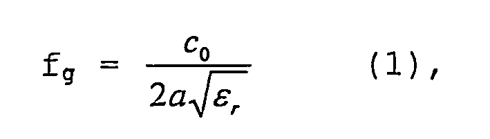
wobei C0 der Lichtgeschwindigkeit im Vakuum (C0 = 3 · 108 m/s), a dem Abstand der Durchkontaktierungseinrichtungen 15 bzw. Via-Wände und εr der dielektrischen Permittivität des Substratmaterials entspricht. Folglich muss die Ungleichung 
erfüllt sein, damit bis zur Frequenz fg kein Hohlleitermode angeregt wird. Der Abstand a ist je nach elektrischer Auswirkung der Formgebung der Vias bzw. deren Abständen sowie des zusätzlichen (vergleichsweise geringen) Einflusses der Signalleitung 10 zu reduzieren.The first propagatable waveguide mode of a rectangular waveguide, which is approximately present here, is the TE 10 mode, a mode with transverse electric field (TE) viewed in cross section. The cutoff frequency of this mode is
where C 0 corresponds to the speed of light in vacuum (C 0 = 3 × 10 8 m / s), a the distance between the via
be satisfied, so that up to the frequency fg no waveguide mode is excited. The distance a is to be reduced depending on the electrical effect of the shape of the vias or their distances and the additional (relatively low) influence of the
Führte man nun diese Via-Wand 15 mit entsprechendem Abstand a parallel zur Signalleitung 10, so würde sich diese Wand 15 im Bereich der Kopplungsöffnung 14 mit dieser orthogonal ausgerichteten Koppelöffnung 14 schneiden, wodurch die Funktionsweise des Koppelschlitzes 14 und damit der Antenne bzw. Übertragungseinrichtung nicht mehr sichergestellt wäre. Daher ist es erforderlich, in der Umgebung des Koppelschlitzes 14 den Abstand der Via-Wände deutlich zu vergrößern, um ihn erst hinter dem Schlitz 14 im Bereich der leerlaufenden Signalleitung 10' wieder auf den ursprünglichen Wert herabsetzen zu können. Hinter dem leerlaufenden Ende 10' der Mikrostreifenleitung 10 wäre dann auch ein Zusammenführen der Via-Wände 15 möglich, jedoch nicht zwangsläufig erforderlich, da aufgrund des dort vorhandenen geringen Abstandes der Via-Wände keine Anregung von Substrat bzw. Hohlleitermoden möglich wäre. Um andererseits eine maximale Schirmwirkung zu erzielen und auch elektromagnetische Einkopplungen von außen in die Anordnung zu verhindern, führt man die Durchkontaktierungseinrichtung 15, d.h. die Wände, longitudinal benachbart der leerlaufenden Signalleitung 10' vorzugsweise zusammen.If this via
Mit Bezug auf die Dimensionierung bzw. Strukturierung der Durchkontaktierungseinrichtung 15 bzw. der Via-Wände im Bereich der Kopplungsöffnung 14 muß berücksichtigt werden, dass bei Vergrößerung des Abstandes a dieser Wände die Grenzfrequenz fg des Hohlleitermodes sinkt, und zwar im allgemeinen unter die Nutzfrequenz f der Antenne selbst, damit die Beeinträchtigung der Funktion der Kopplungsöffnung 14 durch die Via-Wände 15 minimal bzw. in einem Entwurf der Anordnung berücksichtigbar ist. Andererseits birgt dies die Gefahr in sich, dass sich innerhalb dieser Schirmwände 15 mit dem stark vergrößerten Abstand B im Bereich der Kopplungsöffnung 14 Hohlraumresonanzen bilden können, welche die Funktion der Antenne stark beeinträchtigen, wenn diese eventuell auftretenden unerwünschten Resonanzfrequenzen im Nutzfrequenzbereich liegen. Um dieses nun gezielt zu verhindern, ist die Länge L der Via-Wände 15 in X-Richtung im Bereich der Kopplungsöffnung bei dem vergrößerten Abstand B der Schirmwände 15 in Y-Richtung entsprechend zu wählen.With regard to the dimensioning or structuring of the via
In einem vollständig geschlossenen, dielektrisch gefüllten, rechteckigen Hohlleiterresonator der Breite B, der Höhe H sowie der Länge L mit ideal leitenden elektrischen Wänden ergeben sich mögliche diskrete Resonanzfrequenzen gemäß folgendem Zusammenhang: 
, wobei p, m und n ganzzahlige Indizes sind, C0 die Vakuumlichtgeschwindigkeit und εr die dielektrische Permittivität des nichtleitenden Füllmaterials darstellt. Für den hier relevanten TE10-Mode gilt m = 1 sowie n = 0, so dass die möglichen Resonanzfrequenzen zwar von der Breite B, aber nicht von der Höhe H abhängen. Der ganzzahlige Index p muss bei TE-Moden größer als Null sein. Daraus ergibt sich die erste anregbare Hohlraumresonanz des TE10-Modes gemäß 
Wherein p, m and n are integer indices, C 0 is the vacuum velocity of light and ε r is the dielectric permittivity of the dielectric filling material. For the TE 10 mode relevant here, m = 1 and n = 0, so that the possible resonance frequencies depend on the width B, but not on the height H. The integer index p must be greater than zero for TE modes. This results in the first excitable cavity resonance of the TE 10 -mode according to
Im Entwurf der Antenne mit Schlitzkopplung und Via-Abschirmung 15 der Signalleitung 10 ist nun darauf zu achten, dass die Grenzfrequenz der hohlleiterähnlichen Resonanz gemäß Gleichung (1), wobei dann a = B zu setzen ist, zwar unterhalb des Nutzsignalfrequenzbandes F liegen darf, dass aber die erste Resonanzfrequenz gemäß Gleichung (4) oberhalb des Nutzsignalfrequenzbandes F liegen muss, um eine Beeinträchtigung der Funktionsweise der Übertragungseinrichtung 16 und/oder Antenne zu verhindern.In the design of the antenna with slotted coupling and via-shielding 15 of the
Darüber hinaus ist bei vorliegender Ausführungsform gemäß
In
In
Die gemäß
Damit die elektromagnetische Kopplung durch die Kopplungsöffnung 14 von der Abschirmeinrichtung 15 nicht beeinträchtigt wird, ist im Bereich des Koppelschlitzes 14 der Abstand der Via-Wände B auf beispielsweise 3,6 mm erhöht. Die Grenzfrequenz fg des TE10-Modes sinkt dadurch gemäß Gleichung (1) auf etwa 15 GHz. Damit nun die erste Resonanzfrequenz fres dieses Modes oberhalb von beispielsweise 27 GHz liegt, um einen 1 GHz-Frequenzabstand zum Nutzfrequenzband F sicherzustellen, muss gemäß Gleichung (4) die Länge L kleiner als 2,4 mm gewählt werden. Um zusätzlich die oben genannten Beeinflussungen der Resonanzfrequenz fres zu kompensieren, wird L im vorliegenden Ausführungsbeispiel vorzugsweise zu 1,2 mm gewählt.So that the electromagnetic coupling is not impaired by the
In
Planarstrahler, Kopplungsöffnung 14 bzw. Koppelschlitz, Signalleitung 10 und Impedanztransformator 17 einstellen.Planar radiator, coupling
In
Im wesentlichen entspricht die Anordnung im unteren Bereich einer unsymmetrischen Triplate-Speisung, welche jedoch ihr ausgekoppeltes Feld nicht auf einen Planarstrahler (16, hier jedoch nicht dargestellt), sondern in eine weiterführende Streifenleitung 10 überträgt. Auf diese Weise wird folglich kein Antennenelement, sondern eine Kopplungseinrichtung bereitgestellt, welche über eine elektromagnetische Ankopplung eines Signals einer Streifenleitung in einer Ebene das Signal galvanisch getrennt an eine zweite Streifenleitung 10 in einer anderen Ebene überträgt. Die in
In
Obwohl die-vorliegende Erfindung vorstehend anhand bevorzugter Ausführungsbeispiele beschrieben wurde, ist sie darauf nicht beschränkt, sondern, im Rahmen der Ansprüche, auf vielfältige Weise modifizierbar.Although the present invention has been described above with reference to preferred embodiments, it is not limited thereto but, within the scope of the claims, modifiable in a variety of ways.
Insbesondere sind die genannten Materialien für das dielektrische Substrat, die Masseflächen und die Streifenleitung beispielhaft zu sehen. Darüber hinaus ist die Gestaltung der Koppelschlitze, der planaren Kopplungseinrichtung und der Streifenleitung nicht zwangsläufig rechteckig, sondern können auch runde, ovale oder polygonförmige Querschnitte bzw. Draufsichten aufweisen. Insbesondere die Durchkontaktierungseinrichtung bzw. Abschirmwände müssen nicht rechtwinklig zueinander verlaufen, sondern können abgerundete Übergänge aufweisen.In particular, the materials mentioned for the dielectric substrate, the ground areas and the strip line can be seen by way of example. In addition, the design of the coupling slots, the planar coupling device and the strip line is not necessarily rectangular, but may also have round, oval or polygonal cross-sections or plan views. In particular, the through-contact device or shielding walls do not have to run at right angles to each other, but may have rounded transitions.
Claims (18)
- Apparatus for transmission or emission of radio-frequency waves, having:a micro stripline (10), which is provided with an end (10'), in a substrate (11) for transmission of a radio-frequency useful signal;a first ground plane (12) and a second ground plane (13), which are provided on opposite sides of the substrate (11), in order to form a TEM waveguide arrangement;a coupling opening (14) in the first ground plane (12) at a predetermined distance (d) from the end (10') of the stripline (10) for outputting the radio-frequency useful signal;a through-contacting device (15) for conductive connection of the first ground plane (12) to the second ground plane (13) in the side periphery of the coupling opening (14);
wherein the through-contacting device (15) is designed such that, at a given frequency (f) of the useful signal, it prevents the propagation of waveguide modes and the excitation of waveguide mode resonances in a useful frequency band (f) of the useful signal;
anda planar coupling device (16) for reception and transmission or emission of the output radio-frequency useful signal;
characterized in thatthe through-contacting device (15), formed as two walls, extends from both sides and parallel to the micro stripline (10) over a specific length in each of the areas before, in the area of and at the end (10'), after the coupling opening (14), with the walls before and after the coupling opening (14) being at a distance (a) apart, where
- Apparatus according to Claim 1,
characterized in that
the following relationship exists between the greater distance (B) between the walls of the through-contacting device (15) in the area of the coupling opening (14) and the length (L) of the through-contacting device in the area of the coupling opening (14):
where fres is a resonant frequency of a waveguide mode which can be excited and can be provided above the useful signal frequency band (F). - Apparatus according to Claim 2,
characterized in that
the resonant frequency fres is more than a few per cent above the useful signal frequency band (F). - Apparatus according to one of the preceding claims,
characterized in that
the apparatus is designed for useful signals in a useful signal frequency band (F) between 20 GHz and 30 GHz. - Apparatus according to one of the preceding claims, characterized in that
the through-contacting device (15) is composed of discrete through-contacting elements (15') which are arranged laterally adjacent to one another, forming a wall. - Apparatus according to Claim 5,
characterized in that
the discrete through-contacting elements (15') are round and/or cylindrical. - Apparatus according to one of the preceding Claims 1-4,
characterized in that
the through-contacting device (15) forms a continuous wall. - Apparatus according to one of the preceding claims,
characterized in that
the through-contacting device (15) is provided in a continuous form in the area longitudinally adjacent to the end (10') of the stripline (10). - Apparatus according to one of the preceding claims,
characterized in that
the through-contacting device (15) is provided with a gap in the area longitudinally adjacent to the end (10') of the stripline (10). - Apparatus according to one of the preceding claims,
characterized in that
the micro stripline (10) is arranged closer to that ground plane (12) which is provided with the coupling opening (14) than to the other ground plane (13) in the substrate (11), or vice versa. - Apparatus according to one of the preceding Claims 1-9,
characterized in that
the micro stripline (10) is arranged approximately equidistant between that ground plane (12) which is provided with the coupling opening (14) and the other ground plane (13) in the substrate (11). - Apparatus according to one of the preceding claims,
characterized in that
the micro stripline (10) has an integrated impedance transformer (17) in the area of the coupling opening (14). - Apparatus according to one of the preceding claims,
characterized in that
the planar coupling device (16) forms a second micro stripline (10) on another plane, which is provided in a galvanically isolated form, for electromagnetic coupling of this further micro stripline (10). - Apparatus according to Claim 13,
characterized in that
the planar coupling device (16) can be caused to resonate by means of the coupling opening (14), and can therefore be excited for emission. - Apparatus according to Claim 14,
characterized in that
the coupling opening (14) can itself be made to resonate and can thus be excited for emission. - Apparatus according to Claim 15,
characterized in that
the two micro striplines (10) are designed to be essentially identical and overlap by twice a predetermined distance (d) in the longitudinal direction, which distance (d) preferably corresponds to approximately half the wavelength of the coupled useful signal. - Apparatus according to one of the preceding claims,
characterized in that
the coupling opening (14) is provided in the form of a slot and/or in the form of a rectangle parallel to the ground planes (12, 13). - Apparatus according to one of the preceding claims,
characterized in that
the substrate (11) has a ceramic material, preferably low temperature cofired ceramic (LTCC).
Applications Claiming Priority (3)
| Application Number | Priority Date | Filing Date | Title |
|---|---|---|---|
| DE10244206A DE10244206A1 (en) | 2002-09-23 | 2002-09-23 | Wave transfer device for transferring/radiating high-frequency waves has a micro strip transmission line in a substrate to transfer high-frequency wanted signals |
| DE10244206 | 2002-09-23 | ||
| PCT/DE2003/002408 WO2004030141A1 (en) | 2002-09-23 | 2003-07-17 | Device for transmitting or emitting high-frequency waves |
Publications (2)
| Publication Number | Publication Date |
|---|---|
| EP1547192A1 EP1547192A1 (en) | 2005-06-29 |
| EP1547192B1 true EP1547192B1 (en) | 2010-01-20 |
Family
ID=31896308
Family Applications (1)
| Application Number | Title | Priority Date | Filing Date |
|---|---|---|---|
| EP03798044A Expired - Lifetime EP1547192B1 (en) | 2002-09-23 | 2003-07-17 | Device for transmitting or emitting high-frequency waves |
Country Status (5)
| Country | Link |
|---|---|
| US (1) | US7154441B2 (en) |
| EP (1) | EP1547192B1 (en) |
| JP (1) | JP2006500835A (en) |
| DE (2) | DE10244206A1 (en) |
| WO (1) | WO2004030141A1 (en) |
Families Citing this family (27)
| Publication number | Priority date | Publication date | Assignee | Title |
|---|---|---|---|---|
| US6743731B1 (en) * | 2000-11-17 | 2004-06-01 | Agere Systems Inc. | Method for making a radio frequency component and component produced thereby |
| DE102005011127B4 (en) * | 2005-03-10 | 2012-06-21 | Imst Gmbh | Calibration of an electronically controllable planar antenna and electronically controllable planar antenna with one cavity |
| DE102005048274B4 (en) * | 2005-10-08 | 2012-03-22 | Imst Gmbh | Fully integrated miniaturized radar sensor in LTCC multilayer technology with planar dual antenna device |
| KR100758998B1 (en) * | 2006-05-24 | 2007-09-17 | 삼성전자주식회사 | Patch antenna for local area communication |
| JP4131984B2 (en) * | 2006-05-25 | 2008-08-13 | 松下電器産業株式会社 | Variable slot antenna and driving method thereof |
| DE102006039279B4 (en) * | 2006-08-22 | 2013-10-10 | Kathrein-Werke Kg | Dipole radiator arrangement |
| US7292204B1 (en) * | 2006-10-21 | 2007-11-06 | National Taiwan University | Dielectric resonator antenna with a caved well |
| US7626549B2 (en) | 2007-03-28 | 2009-12-01 | Eswarappa Channabasappa | Compact planar antenna for single and multiple polarization configurations |
| DE102008042449A1 (en) * | 2008-09-29 | 2010-04-01 | Robert Bosch Gmbh | Radar sensor with shielded signal stabilizer |
| JP5300583B2 (en) * | 2008-11-19 | 2013-09-25 | 三菱電機株式会社 | Antenna device |
| KR100949972B1 (en) * | 2009-01-02 | 2010-03-29 | 엘지전자 주식회사 | Random access scheme for user equipment |
| JP5309209B2 (en) * | 2009-03-31 | 2013-10-09 | 京セラ株式会社 | Waveguide structure, and high-frequency module and radar apparatus including waveguide structure |
| JP5408160B2 (en) * | 2011-03-09 | 2014-02-05 | 株式会社村田製作所 | Horizontal radiating antenna |
| JP5429215B2 (en) * | 2011-03-09 | 2014-02-26 | 株式会社村田製作所 | Horizontal radiating antenna |
| KR101255947B1 (en) * | 2011-10-05 | 2013-04-23 | 삼성전기주식회사 | Dielectric resonant antenna adjustable bandwidth |
| WO2013189072A1 (en) | 2012-06-21 | 2013-12-27 | Telefonaktiebolaget L M Ericsson (Publ) | Bandpass filter and method of fabricating the same |
| JP6003811B2 (en) * | 2013-06-05 | 2016-10-05 | 日立金属株式会社 | Antenna device |
| DE102013017263A1 (en) * | 2013-10-17 | 2015-04-23 | Valeo Schalter Und Sensoren Gmbh | High-frequency antenna for a motor vehicle radar sensor, radar sensor and motor vehicle |
| KR101693843B1 (en) | 2015-03-03 | 2017-01-10 | 한국과학기술원 | Microstrip Circuit and Single Sideband Transmission Chip-to-Chip Interface using Dielectric Waveguide |
| EP3309897A1 (en) * | 2016-10-12 | 2018-04-18 | VEGA Grieshaber KG | Waveguide coupling for radar antenna |
| US11710904B2 (en) * | 2017-12-26 | 2023-07-25 | Vayyar Imaging Ltd. | Cavity backed antenna with in-cavity resonators |
| EP3582326B1 (en) * | 2018-06-15 | 2021-10-06 | Nokia Solutions and Networks Oy | Antenna coupling |
| RU2688826C1 (en) * | 2018-06-18 | 2019-05-22 | Федеральное государственное автономное образовательное учреждение высшего образования "Сибирский федеральный университет" | Microstrip band-pass filter |
| TWI678844B (en) * | 2018-11-23 | 2019-12-01 | 和碩聯合科技股份有限公司 | Antenna structure |
| CN110233333A (en) * | 2019-04-26 | 2019-09-13 | 中天宽带技术有限公司 | From decoupling antenna |
| CN110364822A (en) * | 2019-08-08 | 2019-10-22 | 天津职业技术师范大学(中国职业培训指导教师进修中心) | The super surface of double frequency c type split ring resonator Terahertz ring dipole and preparation method |
| CN114976602B (en) * | 2022-07-13 | 2022-12-20 | 荣耀终端有限公司 | Planar inverted-F antenna pair and electronic equipment |
Family Cites Families (16)
| Publication number | Priority date | Publication date | Assignee | Title |
|---|---|---|---|---|
| US4197544A (en) * | 1977-09-28 | 1980-04-08 | The United States Of America As Represented By The Secretary Of The Navy | Windowed dual ground plane microstrip antennas |
| US4531130A (en) * | 1983-06-15 | 1985-07-23 | Sanders Associates, Inc. | Crossed tee-fed slot antenna |
| JP3064395B2 (en) * | 1990-11-05 | 2000-07-12 | 三菱電機株式会社 | Microstrip antenna |
| JPH04284004A (en) * | 1991-03-13 | 1992-10-08 | Toshiba Corp | Planer antenna |
| US5241321A (en) | 1992-05-15 | 1993-08-31 | Space Systems/Loral, Inc. | Dual frequency circularly polarized microwave antenna |
| JPH10303612A (en) * | 1997-04-25 | 1998-11-13 | Kyocera Corp | Patch antenna |
| JPH11136022A (en) * | 1997-10-29 | 1999-05-21 | Mitsubishi Electric Corp | Antenna device |
| US6181279B1 (en) * | 1998-05-08 | 2001-01-30 | Northrop Grumman Corporation | Patch antenna with an electrically small ground plate using peripheral parasitic stubs |
| JP2000174515A (en) * | 1998-12-10 | 2000-06-23 | Sumitomo Metal Ind Ltd | Coplanar waveguide - waveguide converter |
| JP2000261235A (en) * | 1999-03-05 | 2000-09-22 | Mitsubishi Electric Corp | Triplate line feeding type microstrip antenna |
| US6507320B2 (en) | 2000-04-12 | 2003-01-14 | Raytheon Company | Cross slot antenna |
| DE10063437A1 (en) * | 2000-12-20 | 2002-07-11 | Bosch Gmbh Robert | antenna array |
| US6492947B2 (en) | 2001-05-01 | 2002-12-10 | Raytheon Company | Stripline fed aperture coupled microstrip antenna |
| WO2003052686A2 (en) | 2001-12-14 | 2003-06-26 | Seagate Technology Llc | Initial learn of adaptive feedforward coefficients |
| BG64431B1 (en) * | 2001-12-19 | 2005-01-31 | Skygate International Technology N.V. | Antenna element |
| GB2387036B (en) * | 2002-03-26 | 2005-03-02 | Ngk Spark Plug Co | Dielectric antenna |
-
2002
- 2002-09-23 DE DE10244206A patent/DE10244206A1/en not_active Withdrawn
-
2003
- 2003-07-17 EP EP03798044A patent/EP1547192B1/en not_active Expired - Lifetime
- 2003-07-17 DE DE50312367T patent/DE50312367D1/en not_active Expired - Lifetime
- 2003-07-17 JP JP2004538683A patent/JP2006500835A/en active Pending
- 2003-07-17 US US10/514,262 patent/US7154441B2/en not_active Expired - Fee Related
- 2003-07-17 WO PCT/DE2003/002408 patent/WO2004030141A1/en active Application Filing
Also Published As
| Publication number | Publication date |
|---|---|
| US7154441B2 (en) | 2006-12-26 |
| WO2004030141A1 (en) | 2004-04-08 |
| US20050219123A1 (en) | 2005-10-06 |
| EP1547192A1 (en) | 2005-06-29 |
| JP2006500835A (en) | 2006-01-05 |
| DE10244206A1 (en) | 2004-03-25 |
| DE50312367D1 (en) | 2010-03-11 |
Similar Documents
| Publication | Publication Date | Title |
|---|---|---|
| EP1547192B1 (en) | Device for transmitting or emitting high-frequency waves | |
| DE102017103161B4 (en) | Antenna device and antenna array | |
| DE60009874T2 (en) | V-slot antenna for circular polarization | |
| DE112004000077B4 (en) | Twisted waveguide and wireless device | |
| DE69933085T2 (en) | Radio communication device and a slot loop antenna | |
| DE69821884T2 (en) | Multifrequency stripline antenna and device with such an antenna | |
| DE102009035359B4 (en) | Microstrip antenna array | |
| EP0766099B1 (en) | Doppler radar module | |
| DE60302766T2 (en) | WAVEGUIDE | |
| EP1842263B1 (en) | Planar multiband antenna | |
| DE10350346B4 (en) | High Frequency Line Waveguide Converter and High Frequency Package | |
| DE69826223T2 (en) | Microstrip line antenna and antenna containing device | |
| DE102013012315B4 (en) | Waveguide radiators. Group Antenna Emitter and Synthetic Aperture Radar System | |
| DE69936903T2 (en) | Antenna for two frequencies for radio communication in the form of a microstrip antenna | |
| AT508750B1 (en) | DEVICE FOR TRANSFERRING HIGH-FREQUENCY SIGNALS | |
| EP2991159B1 (en) | Feed network for antenna systems | |
| DE112009001891T5 (en) | High frequency substrate and high frequency module | |
| EP0101611A2 (en) | Transmitter-receiver module | |
| DE112018006818T5 (en) | WAVELINE-MICROSTRIPLINE CONVERTER AND ANTENNA DEVICE | |
| DE102019134670A1 (en) | WAVE GUIDE DEVICE, ANTENNA DEVICE AND COMMUNICATION DEVICE | |
| DE19729664C2 (en) | Planar broadband antenna | |
| DE10065510A1 (en) | Resonator, resonator element, resonator device, filter, duplexer and communication device | |
| DE102008026579B4 (en) | Angled transition from microstrip line to rectangular waveguide | |
| DE19941881C2 (en) | Dielectric filter, dielectric duplexer and transceiver | |
| DE112020007004T5 (en) | PHASE SHIFTER AND ANTENNA |
Legal Events
| Date | Code | Title | Description |
|---|---|---|---|
| PUAI | Public reference made under article 153(3) epc to a published international application that has entered the european phase |
Free format text: ORIGINAL CODE: 0009012 |
|
| 17P | Request for examination filed |
Effective date: 20050425 |
|
| AK | Designated contracting states |
Kind code of ref document: A1 Designated state(s): AT BE BG CH CY CZ DE DK EE ES FI FR GB GR HU IE IT LI LU MC NL PT RO SE SI SK TR |
|
| RBV | Designated contracting states (corrected) |
Designated state(s): DE ES FR GB IT SE |
|
| 17Q | First examination report despatched |
Effective date: 20060707 |
|
| GRAP | Despatch of communication of intention to grant a patent |
Free format text: ORIGINAL CODE: EPIDOSNIGR1 |
|
| GRAS | Grant fee paid |
Free format text: ORIGINAL CODE: EPIDOSNIGR3 |
|
| GRAA | (expected) grant |
Free format text: ORIGINAL CODE: 0009210 |
|
| AK | Designated contracting states |
Kind code of ref document: B1 Designated state(s): DE ES FR GB IT SE |
|
| REG | Reference to a national code |
Ref country code: GB Ref legal event code: FG4D Free format text: NOT ENGLISH |
|
| REF | Corresponds to: |
Ref document number: 50312367 Country of ref document: DE Date of ref document: 20100311 Kind code of ref document: P |
|
| PG25 | Lapsed in a contracting state [announced via postgrant information from national office to epo] |
Ref country code: ES Free format text: LAPSE BECAUSE OF FAILURE TO SUBMIT A TRANSLATION OF THE DESCRIPTION OR TO PAY THE FEE WITHIN THE PRESCRIBED TIME-LIMIT Effective date: 20100501 |
|
| PG25 | Lapsed in a contracting state [announced via postgrant information from national office to epo] |
Ref country code: SE Free format text: LAPSE BECAUSE OF FAILURE TO SUBMIT A TRANSLATION OF THE DESCRIPTION OR TO PAY THE FEE WITHIN THE PRESCRIBED TIME-LIMIT Effective date: 20100120 |
|
| PLBE | No opposition filed within time limit |
Free format text: ORIGINAL CODE: 0009261 |
|
| STAA | Information on the status of an ep patent application or granted ep patent |
Free format text: STATUS: NO OPPOSITION FILED WITHIN TIME LIMIT |
|
| 26N | No opposition filed |
Effective date: 20101021 |
|
| PG25 | Lapsed in a contracting state [announced via postgrant information from national office to epo] |
Ref country code: IT Free format text: LAPSE BECAUSE OF FAILURE TO SUBMIT A TRANSLATION OF THE DESCRIPTION OR TO PAY THE FEE WITHIN THE PRESCRIBED TIME-LIMIT Effective date: 20100120 |
|
| REG | Reference to a national code |
Ref country code: FR Ref legal event code: PLFP Year of fee payment: 13 |
|
| PGFP | Annual fee paid to national office [announced via postgrant information from national office to epo] |
Ref country code: GB Payment date: 20150724 Year of fee payment: 13 |
|
| PGFP | Annual fee paid to national office [announced via postgrant information from national office to epo] |
Ref country code: FR Payment date: 20150730 Year of fee payment: 13 |
|
| GBPC | Gb: european patent ceased through non-payment of renewal fee |
Effective date: 20160717 |
|
| PG25 | Lapsed in a contracting state [announced via postgrant information from national office to epo] |
Ref country code: FR Free format text: LAPSE BECAUSE OF NON-PAYMENT OF DUE FEES Effective date: 20160801 |
|
| REG | Reference to a national code |
Ref country code: FR Ref legal event code: ST Effective date: 20170331 |
|
| PG25 | Lapsed in a contracting state [announced via postgrant information from national office to epo] |
Ref country code: GB Free format text: LAPSE BECAUSE OF NON-PAYMENT OF DUE FEES Effective date: 20160717 |
|
| PGFP | Annual fee paid to national office [announced via postgrant information from national office to epo] |
Ref country code: DE Payment date: 20190924 Year of fee payment: 17 |
|
| REG | Reference to a national code |
Ref country code: DE Ref legal event code: R119 Ref document number: 50312367 Country of ref document: DE |
|
| PG25 | Lapsed in a contracting state [announced via postgrant information from national office to epo] |
Ref country code: DE Free format text: LAPSE BECAUSE OF NON-PAYMENT OF DUE FEES Effective date: 20210202 |