EP1545165B1 - Discharge lamp driving circuit provided with discharge detecting pattern - Google Patents
Discharge lamp driving circuit provided with discharge detecting pattern Download PDFInfo
- Publication number
- EP1545165B1 EP1545165B1 EP04257799A EP04257799A EP1545165B1 EP 1545165 B1 EP1545165 B1 EP 1545165B1 EP 04257799 A EP04257799 A EP 04257799A EP 04257799 A EP04257799 A EP 04257799A EP 1545165 B1 EP1545165 B1 EP 1545165B1
- Authority
- EP
- European Patent Office
- Prior art keywords
- discharge
- discharge lamp
- driving circuit
- transformer
- pattern
- Prior art date
- Legal status (The legal status is an assumption and is not a legal conclusion. Google has not performed a legal analysis and makes no representation as to the accuracy of the status listed.)
- Not-in-force
Links
- 230000006698 induction Effects 0.000 claims description 14
- 230000004907 flux Effects 0.000 claims description 3
- 238000010891 electric arc Methods 0.000 description 10
- 238000010586 diagram Methods 0.000 description 8
- 239000004973 liquid crystal related substance Substances 0.000 description 5
- 210000002858 crystal cell Anatomy 0.000 description 3
- 230000002950 deficient Effects 0.000 description 2
- 238000001514 detection method Methods 0.000 description 2
- 238000000034 method Methods 0.000 description 2
- 230000010355 oscillation Effects 0.000 description 2
- 238000000059 patterning Methods 0.000 description 2
- 230000035945 sensitivity Effects 0.000 description 2
- 239000003990 capacitor Substances 0.000 description 1
- 238000010304 firing Methods 0.000 description 1
- 238000009413 insulation Methods 0.000 description 1
- 230000010354 integration Effects 0.000 description 1
- 229910001507 metal halide Inorganic materials 0.000 description 1
- 150000005309 metal halides Chemical class 0.000 description 1
- 230000001012 protector Effects 0.000 description 1
- 230000000391 smoking effect Effects 0.000 description 1
Images


Classifications
-
- H—ELECTRICITY
- H05—ELECTRIC TECHNIQUES NOT OTHERWISE PROVIDED FOR
- H05B—ELECTRIC HEATING; ELECTRIC LIGHT SOURCES NOT OTHERWISE PROVIDED FOR; CIRCUIT ARRANGEMENTS FOR ELECTRIC LIGHT SOURCES, IN GENERAL
- H05B41/00—Circuit arrangements or apparatus for igniting or operating discharge lamps
- H05B41/14—Circuit arrangements
- H05B41/26—Circuit arrangements in which the lamp is fed by power derived from DC by means of a converter, e.g. by high-voltage DC
- H05B41/28—Circuit arrangements in which the lamp is fed by power derived from DC by means of a converter, e.g. by high-voltage DC using static converters
- H05B41/282—Circuit arrangements in which the lamp is fed by power derived from DC by means of a converter, e.g. by high-voltage DC using static converters with semiconductor devices
- H05B41/285—Arrangements for protecting lamps or circuits against abnormal operating conditions
- H05B41/2851—Arrangements for protecting lamps or circuits against abnormal operating conditions for protecting the circuit against abnormal operating conditions
- H05B41/2856—Arrangements for protecting lamps or circuits against abnormal operating conditions for protecting the circuit against abnormal operating conditions against internal abnormal circuit conditions
Definitions
- the present invention relates to a discharge lamp driving circuit for lighting a discharge lamp to illuminate a liquid crystal display (LCD) apparatus, and more specifically to a discharge lamp driving circuit provided with a function of detecting electric discharges, such as an arc discharge, and a corona discharge, that occur in the circuit.
- a discharge lamp driving circuit provided with a function of detecting electric discharges, such as an arc discharge, and a corona discharge, that occur in the circuit.
- a backlight system has been generally used as a lighting device for an LCD apparatus.
- the backlight system comprises: one or more discharge lamp, such as a cold cathode lamp and a metal halide lamps; and a discharge lamp driving circuit composed of various circuits, such as an inverter circuit to drive the discharge lamp. Since a high voltage is required for lighting the discharge lamp, the discharge lamp driving circuit has a high-voltage transformer, and the discharge lamp is connected to the secondary side of the high-voltage transformer.
- the discharge lamp driving circuit is equipped with a protector by which the circuit is deactivated, for example, when a lamp current flowing in the discharge lamp has an abnormally high value.
- a protection circuit is activated thereby preventing an overcurrent from flowing in the discharge lamp (refer to, for example, Japanese Patent Application Laid-Open No. 2003-168585 ) .
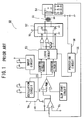
- Fig. 1 is a block diagram showing a discharge lamp driving circuit 50 disclosed in the aforementioned Japanese Patent Application Laid-Open No. 2003-168585 .
- the primary side of a transformer 51 is connected to an H-bridge circuit 52 which drives the primary side of the transformer 51, and to which a logic circuit 53 to produce a signal to be sent to the H-bridge 52 is connected, while the secondary side of the transformer 51 is connected to a discharge lamp 54, and also to a protection circuit 55 which, when a voltage of a signal 56 at the secondary side of the transformer 51 exceeds a predetermined value, deactivates the logic circuit 53 thereby preventing an overcurrent from flowing in the discharge lamp 54.
- a high-voltage transformer is provided in a discharge lamp driving circuit. So, if a withstand voltage is lowered due to poor connection of a wiring to the secondary terminal of the transformer, breakage of a wiring at the secondary side of the transformer, poor connection between connector terminals for the discharge lamp, defective wires of the discharge lamp, or poor insulation of coils in the transformer, then an arc discharge, or a corona discharge can occur at some small gaps or voids found at the defective or poor areas.
- the arc discharge is accompanied by sparks, and may damage terminals and components, or even cause smoking or firing, resulting in possibly damaging the discharge lamp driving circuit and the LCD apparatus.
- the logic circuit 53 is deactivated when the voltage of the signal 56 at the secondary side of the transformer 51 exceeds a predetermined value, whereby an overcurrent is prevented from flowing in the discharge lamp 54.
- the discharge lamp 54 is kept on lighting even if a corona discharge or an arc discharge occurs at partially broken wires at the secondary side of the transformer 51, the lamp current is kept at a constant value, and therefore the protection circuit 55 fails to duly function. Thus, the discharge cannot be detected.
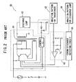
- a discharge lamp driving circuit in which a corona discharge occurring near a high-voltage transformer or a discharge lamp is detected at its very start for protection of the circuit (refer to, for example, Japanese Patent Application Laid-Open No. 2002-341775 ).
- Such a discharge lamp driving circuit includes an induction pattern for a transformer, and another induction pattern for a discharge lamp, and voltages induced in the induction patterns are detected for protection of an inverter circuit.
- Fig. 2 is a block diagram showing a discharge lamp driving circuit 60 disclosed in the aforementioned Japanese Patent Application Laid-Open No. 2002-341775 .
- the discharge lamp driving circuit 60 has an induction pattern 62 for a transformer shaped into an elongated rectangle and disposed at an area in the lower face of a printed circuit board corresponding to a high-voltage transformer 61, and an induction pattern 64 for a discharge lamp shaped into a rectangle and disposed at an areas in the lower face of a printed circuit board corresponding a discharge lamp 63.
- the discharge lamp driving circuit as described above is formed on a printed circuit board which is dimensioned substantially as large as a light conductive plate disposed on the bottom face of a liquid crystal cell, the printed circuit board has to be inevitably dimensioned as large as the liquid crystal cell. Consequently, in a large LCD apparatus used in, for example, a large TV, a large printed circuit board must be used in accordance with the size of the liquid crystal cell, which results in an increased cost of the discharge lamp driving circuit. Also, respective induction patterns must be disposed for a transformer and a discharge lamp thus constituting another factor for an increased cost.
- the present invention has been made in light of the above problems.
- a discharge lamp driving circuit as claimed in claim 1. It is an object of the present invention to provide a discharge lamp driving circuit which is deactivated upon detection of a discharge occurring at a wiring at the secondary side of a high-voltage transformer, and which is produced inexpensively for use in a large LCD apparatus.
- the discharge lamp driving circuit comprises: a control circuit; a transformer having one end of at least one discharge lamp connected to one end of a secondary side thereof; a transformer driving circuit to drive a primary side of the transformer for lighting the at least one discharge lamp; a current-voltage converting circuit provided at the other end of the at least one discharge lamp and functioning to convert a lamp current to a voltage; and a lamp current controlling pattern provided at the other end of the at least one discharge lamp.
- a discharge detecting pattern is further provided at a grounding end of the secondary side of the transformer so as to be located close to and in parallel with the lamp current controlling pattern, whereby a voltage induced at the discharge detecting pattern is detected thereby stopping supply of electric power to the secondary side of the transformer.
- a corona discharge or an arc discharge can be detected through a voltage induced in the discharge detecting pattern by a high-frequency noise component of the lamp current flowing in the lamp current controlling pattern, whereby the discharge lamp driving circuit is deactivated and protected.
- the lamp current controlling pattern and the discharge detecting pattern may be formed on one same surface of a printed circuit board. Consequently, if they are formed on the same surface that has electronic components such as the control circuit, the transformer, and the transformer driving circuit formed thereon, then the patterning work can be done coincidentally with the circuit wiring work thereby improving the working process.
- the lamp current controlling pattern and the discharge detecting pattern may be formed in a zigzag line. Consequently, the pattern inductance can be arbitrarily adjusted for detecting with an enhanced efficiency.
- More than one discharge lamp may be connected to the secondary side of the transformer. Thus, multiple discharge lamps can be lighted simultaneously.
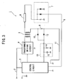
- a transformer driving circuit 4 is connected to the primary side of a transformer 5 and drives the primary side of the transformer 5, and a control circuit 3 to control the discharge lamp driving circuit 1 is connected to the transformer driving circuit 4, has an oscillation circuit to set a drive frequency for driving the primary side of the transformer 5, and outputs a control signal sent to the transformer driving circuit 4.
- the transformer driving circuit 4 has switching elements to drive the primary side of the transformer 5.
- an H-bridge is constituted by four switching elements as shown in Fig. 1
- an output signal from the control circuit 3 becomes a gate signal and is inputted into the H-bridge so as to switch the four switching elements at a predetermined time interval thereby generating an alternating voltage which lights a discharge lamp 6 connected to the secondary side of the transformer 5.
- An input voltage line 2 is connected to the control circuit 3 and the transformer driving circuit 4.
- the transformer driving circuit 4 is not limited to the H-bridge as shown in Fig. 1, but may be a half-bridge, or any circuit as long as switching elements to drive the primary side of the transformer 5 are provided.
- the discharge lamp 6 connected to the secondary side of the transformer 5 constitutes a backlight system for use in an LCD apparatus, and may be, for example, a cold cathode lamp.
- One end of the discharge lamp 6 is connected to the secondary side of the transformer 5 as described above while the other end thereof is connected to a current-voltage converting circuit 7 to convert a lamp current flowing in the discharge lamp 6 into a voltage, and an output signal from the current-voltage converting circuit 7 is sent to the control circuit 3 via a lamp current controlling pattern 8 connected to the current-voltage converting circuit 7.
- the control circuit 3 controls the lamp current flowing in the discharge lamp 6 for keeping the current constant.
- An overcurrent detecting resistor 9 and an overcurrent detecting diode 10 are connected to the grounding end of the secondary side of the transformer 5, and the control circuit 3 is connected to the overcurrent detecting resistor 9 and the overcurrent detecting diode 10. Also, a discharge detecting pattern 11 is provided at the grounding end so as to be located close to and in parallel with the lamp current controlling pattern 8, and one end of the discharge detecting pattern 11 is connected to a discharge detecting diode 12 while the other end thereof is grounded.
- the change of the magnetic flux has influence on the discharge detecting pattern 11 disposed parallel to the lamp current controlling pattern 8, and a spike-like induced voltage is generated in the discharge detecting pattern 11.
- the induced voltage goes through the discharge detecting diode 12, and an integration circuit 13 composed of a resistor 14 and a capacitor 15, and is inputted in a comparison circuit provided in the control circuit 3 and compared thereat with a predetermined reference voltage. If the induced voltage exceeds the reference voltage, then the comparison circuit outputs a signal to deactivate the oscillation circuit provided in the control circuit 3 thereby stopping the corona discharge or the arc discharge from going on.
- the discharge lamp driving circuit 1 can be protected.
- the discharge detecting pattern 11 is preferably disposed as close to the lamp current controlling pattern 8 as possible so that the corona discharge or the arc discharge can be detected with an increased sensitivity. Also, the dimension of the parallel disposition of the discharge detecting pattern 11 with respect to the lamp current controlling pattern 8 should be as large as possible for an increased sensitivity.
- the discharge detecting pattern 11 and the lamp current controlling pattern 8 may be formed on either surface of a printed circuit board (not shown), for example such that the discharge detecting pattern 11 is formed on an area of one surface of the printed circuit board corresponding to an area of the other surface having the lamp current controlling pattern 8 formed thereon, but if they are both formed on a surface thereof having electronic components such as the control circuit 3, the transformer driving circuit 4, and the transformer 5 disposed thereon, then the patterning work can coincide with the circuit wiring work thus improving the working process.
- the discharge detecting pattern 11 does not have to be formed in a straight line but alternatively in a zigzag line, or in a twisted line using through-holes in the printed circuit board (not shown).
- the pattern inductance can be adjusted appropriately for detecting discharge with an enhanced efficiency.
- a discharge lamp driving circuit 20 is adapted to drive two discharge lamps 6 connected to the secondary side of a transformer 5.
- the discharge lamp driving circuit 20 operates in the same way as the discharge lamp driving circuit 1 of the first embodiment, and a description thereof will be omitted.
- a discharge lamp driving circuit 30 according to a third embodiment of the present invention is adapted to drive more than two (four in the figure) discharge lamps 6 connected to the secondary side of a transformer 5.
- the discharge lamp driving circuit 30 operates in the same way as the discharge lamp driving circuit 1 of the first embodiment, and a description thereof will be omitted.
- a discharge lamp driving circuit 40 is structured in the same way as the discharge lamp driving circuit 1 of the first embodiment except that the overcurrent detecting resistor 9 and the overcurrent detecting diode 10 are not provided. That is to say, only a discharge detecting function is provided at the grounding end of the secondary side of a transformer 5.
- the discharge lamp driving circuit 40 operates in the same way as the discharge lamp driving circuit 1 of the first embodiment, and a description thereof will be omitted.
Landscapes
- Circuit Arrangements For Discharge Lamps (AREA)
Description
- The present invention relates to a discharge lamp driving circuit for lighting a discharge lamp to illuminate a liquid crystal display (LCD) apparatus, and more specifically to a discharge lamp driving circuit provided with a function of detecting electric discharges, such as an arc discharge, and a corona discharge, that occur in the circuit.
- A backlight system has been generally used as a lighting device for an LCD apparatus. The backlight system comprises: one or more discharge lamp, such as a cold cathode lamp and a metal halide lamps; and a discharge lamp driving circuit composed of various circuits, such as an inverter circuit to drive the discharge lamp. Since a high voltage is required for lighting the discharge lamp, the discharge lamp driving circuit has a high-voltage transformer, and the discharge lamp is connected to the secondary side of the high-voltage transformer. The discharge lamp driving circuit is equipped with a protector by which the circuit is deactivated, for example, when a lamp current flowing in the discharge lamp has an abnormally high value. In such a discharge lamp driving circuit, when a lamp current flowing in the discharge lamp exceeds a predetermined value and it is duly detected, a protection circuit is activated thereby preventing an overcurrent from flowing in the discharge lamp (refer to, for example,
Japanese Patent Application Laid-Open No. 2003-168585 - Fig. 1 is a block diagram showing a discharge
lamp driving circuit 50 disclosed in the aforementionedJapanese Patent Application Laid-Open No. 2003-168585 circuit 50, the primary side of atransformer 51 is connected to an H-bridge circuit 52 which drives the primary side of thetransformer 51, and to which alogic circuit 53 to produce a signal to be sent to the H-bridge 52 is connected, while the secondary side of thetransformer 51 is connected to adischarge lamp 54, and also to aprotection circuit 55 which, when a voltage of asignal 56 at the secondary side of thetransformer 51 exceeds a predetermined value, deactivates thelogic circuit 53 thereby preventing an overcurrent from flowing in thedischarge lamp 54. - Since the discharge lamp used in a backlight system as a lighting device for an LCD apparatus must be driven by a high voltage, a high-voltage transformer is provided in a discharge lamp driving circuit. So, if a withstand voltage is lowered due to poor connection of a wiring to the secondary terminal of the transformer, breakage of a wiring at the secondary side of the transformer, poor connection between connector terminals for the discharge lamp, defective wires of the discharge lamp, or poor insulation of coils in the transformer, then an arc discharge, or a corona discharge can occur at some small gaps or voids found at the defective or poor areas. The arc discharge is accompanied by sparks, and may damage terminals and components, or even cause smoking or firing, resulting in possibly damaging the discharge lamp driving circuit and the LCD apparatus. Therefore, in a discharge lamp driving circuit provided with a high-voltage transformer, it is necessary to detect a corona discharge or an arc discharge, and to stop supplying electric power to a discharge lamp upon detection of such discharges thereby preventing damages to the circuit and the LCD apparatus.
- In the discharge
lamp driving circuit 50 described above, thelogic circuit 53 is deactivated when the voltage of thesignal 56 at the secondary side of thetransformer 51 exceeds a predetermined value, whereby an overcurrent is prevented from flowing in thedischarge lamp 54. However, since thedischarge lamp 54 is kept on lighting even if a corona discharge or an arc discharge occurs at partially broken wires at the secondary side of thetransformer 51, the lamp current is kept at a constant value, and therefore theprotection circuit 55 fails to duly function. Thus, the discharge cannot be detected. - An inverter circuit corresponding to the circuit shown in Figure 1 is also disclosed in
EP 1 296 542 - It is required that a discharge occurring at partially broken wires at the secondary side of a high-voltage transformer be detected in order to stop supply of electric power for the purpose of protecting the circuit. Under the circumstances, a discharge lamp driving circuit is proposed, in which a corona discharge occurring near a high-voltage transformer or a discharge lamp is detected at its very start for protection of the circuit (refer to, for example,
Japanese Patent Application Laid-Open No. 2002-341775 - Fig. 2 is a block diagram showing a discharge
lamp driving circuit 60 disclosed in the aforementionedJapanese Patent Application Laid-Open No. 2002-341775 lamp driving circuit 60 has aninduction pattern 62 for a transformer shaped into an elongated rectangle and disposed at an area in the lower face of a printed circuit board corresponding to a high-voltage transformer 61, and aninduction pattern 64 for a discharge lamp shaped into a rectangle and disposed at an areas in the lower face of a printed circuit board corresponding adischarge lamp 63. When a corona discharge occurs at thetransformer 61 or thedischarge lamp 63, voltages induced at theinduction patterns discharge detecting circuits circuit 60. - Since the discharge lamp driving circuit as described above is formed on a printed circuit board which is dimensioned substantially as large as a light conductive plate disposed on the bottom face of a liquid crystal cell, the printed circuit board has to be inevitably dimensioned as large as the liquid crystal cell. Consequently, in a large LCD apparatus used in, for example, a large TV, a large printed circuit board must be used in accordance with the size of the liquid crystal cell, which results in an increased cost of the discharge lamp driving circuit. Also, respective induction patterns must be disposed for a transformer and a discharge lamp thus constituting another factor for an increased cost. Further, since a plurality of transformers and discharge lamps are provided in a large LCD apparatus, typically in a liquid crystal TV, a plurality of induction patterns must be provided for a transformer and a discharge lamp, respectively, which results in requirement of a number of induction patterns, and also which makes the induction pattern arrangement difficult.
- The present invention has been made in light of the above problems.
- According to the present invention there is provided a discharge lamp driving circuit as claimed in
claim 1. It is an object of the present invention to provide a discharge lamp driving circuit which is deactivated upon detection of a discharge occurring at a wiring at the secondary side of a high-voltage transformer, and which is produced inexpensively for use in a large LCD apparatus. - The discharge lamp driving circuit comprises: a control circuit; a transformer having one end of at least one discharge lamp connected to one end of a secondary side thereof; a transformer driving circuit to drive a primary side of the transformer for lighting the at least one discharge lamp; a current-voltage converting circuit provided at the other end of the at least one discharge lamp and functioning to convert a lamp current to a voltage; and a lamp current controlling pattern provided at the other end of the at least one discharge lamp. A discharge detecting pattern is further provided at a grounding end of the secondary side of the transformer so as to be located close to and in parallel with the lamp current controlling pattern, whereby a voltage induced at the discharge detecting pattern is detected thereby stopping supply of electric power to the secondary side of the transformer. With the structure described above, a corona discharge or an arc discharge can be detected through a voltage induced in the discharge detecting pattern by a high-frequency noise component of the lamp current flowing in the lamp current controlling pattern, whereby the discharge lamp driving circuit is deactivated and protected.
- The lamp current controlling pattern and the discharge detecting pattern may be formed on one same surface of a printed circuit board. Consequently, if they are formed on the same surface that has electronic components such as the control circuit, the transformer, and the transformer driving circuit formed thereon, then the patterning work can be done coincidentally with the circuit wiring work thereby improving the working process.
- The lamp current controlling pattern and the discharge detecting pattern may be formed in a zigzag line. Consequently, the pattern inductance can be arbitrarily adjusted for detecting with an enhanced efficiency.
- More than one discharge lamp may be connected to the secondary side of the transformer. Thus, multiple discharge lamps can be lighted simultaneously.
- Fig. 1 is a block diagram showing a conventional discharge lamp driving circuit;
- Fig. 2 is a block diagram showing another conventional discharge lamp driving circuit;
- Fig. 3 is a block diagram showing a discharge lamp driving circuit according to a first embodiment of the present invention;
- Fig. 4 is a block diagram showing a discharge lamp driving circuit according to a second embodiment of the present invention;
- Fig. 5 is a block diagram showing a discharge lamp driving circuit according to a third embodiment of the present invention; and
- Fig. 6 is a block diagram showing a discharge lamp driving circuit according to a fourth embodiment of the present invention.
- Preferred embodiments of the present invention will hereinafter be described with reference to the accompanying drawings.
- Referring to Fig. 3, in a discharge
lamp driving circuit 1 according to a first embodiment of the present invention, a transformer driving circuit 4 is connected to the primary side of atransformer 5 and drives the primary side of thetransformer 5, and a control circuit 3 to control the dischargelamp driving circuit 1 is connected to the transformer driving circuit 4, has an oscillation circuit to set a drive frequency for driving the primary side of thetransformer 5, and outputs a control signal sent to the transformer driving circuit 4. - The transformer driving circuit 4 has switching elements to drive the primary side of the
transformer 5. For example, if an H-bridge is constituted by four switching elements as shown in Fig. 1, an output signal from the control circuit 3 becomes a gate signal and is inputted into the H-bridge so as to switch the four switching elements at a predetermined time interval thereby generating an alternating voltage which lights adischarge lamp 6 connected to the secondary side of thetransformer 5. An input voltage line 2 is connected to the control circuit 3 and the transformer driving circuit 4. - The transformer driving circuit 4 is not limited to the H-bridge as shown in Fig. 1, but may be a half-bridge, or any circuit as long as switching elements to drive the primary side of the
transformer 5 are provided. - The
discharge lamp 6 connected to the secondary side of thetransformer 5 constitutes a backlight system for use in an LCD apparatus, and may be, for example, a cold cathode lamp. One end of thedischarge lamp 6 is connected to the secondary side of thetransformer 5 as described above while the other end thereof is connected to a current-voltage converting circuit 7 to convert a lamp current flowing in thedischarge lamp 6 into a voltage, and an output signal from the current-voltage converting circuit 7 is sent to the control circuit 3 via a lamp current controllingpattern 8 connected to the current-voltage converting circuit 7. With the output signal from the current-voltage converting circuit 7, the control circuit 3 controls the lamp current flowing in thedischarge lamp 6 for keeping the current constant. - An
overcurrent detecting resistor 9 and anovercurrent detecting diode 10 are connected to the grounding end of the secondary side of thetransformer 5, and the control circuit 3 is connected to the overcurrent detectingresistor 9 and theovercurrent detecting diode 10. Also, adischarge detecting pattern 11 is provided at the grounding end so as to be located close to and in parallel with the lamp current controllingpattern 8, and one end of thedischarge detecting pattern 11 is connected to adischarge detecting diode 12 while the other end thereof is grounded. - Description will hereinafter be made on a discharge detecting operation in case of a corona discharge or an arc discharge occurring at a partially broken wire at the secondary side of the
transformer 5. - When a corona discharge or an arc discharge occurs at a partially broken wire at the secondary side of the
transformer 5, a noise component gets in a lamp current. Since the noise component resulting from the discharge contains a high-frequency component, magnetic flux which is generated by the high-frequency component in the lamp current controllingpattern 8 is caused to change rapidly. - The change of the magnetic flux has influence on the
discharge detecting pattern 11 disposed parallel to the lamp current controllingpattern 8, and a spike-like induced voltage is generated in thedischarge detecting pattern 11. The induced voltage goes through thedischarge detecting diode 12, and anintegration circuit 13 composed of a resistor 14 and acapacitor 15, and is inputted in a comparison circuit provided in the control circuit 3 and compared thereat with a predetermined reference voltage. If the induced voltage exceeds the reference voltage, then the comparison circuit outputs a signal to deactivate the oscillation circuit provided in the control circuit 3 thereby stopping the corona discharge or the arc discharge from going on. Thus, the dischargelamp driving circuit 1 can be protected. - The
discharge detecting pattern 11 is preferably disposed as close to the lamp current controllingpattern 8 as possible so that the corona discharge or the arc discharge can be detected with an increased sensitivity. Also, the dimension of the parallel disposition of thedischarge detecting pattern 11 with respect to the lamp currentcontrolling pattern 8 should be as large as possible for an increased sensitivity. - The
discharge detecting pattern 11 and the lamp currentcontrolling pattern 8 may be formed on either surface of a printed circuit board (not shown), for example such that thedischarge detecting pattern 11 is formed on an area of one surface of the printed circuit board corresponding to an area of the other surface having the lamp currentcontrolling pattern 8 formed thereon, but if they are both formed on a surface thereof having electronic components such as the control circuit 3, the transformer driving circuit 4, and thetransformer 5 disposed thereon, then the patterning work can coincide with the circuit wiring work thus improving the working process. - The
discharge detecting pattern 11 does not have to be formed in a straight line but alternatively in a zigzag line, or in a twisted line using through-holes in the printed circuit board (not shown). When thedischarge detecting pattern 11 is formed in a zigzag line, the pattern inductance can be adjusted appropriately for detecting discharge with an enhanced efficiency. - Referring now to Fig. 4, a discharge
lamp driving circuit 20 according to a second embodiment of the present invention is adapted to drive twodischarge lamps 6 connected to the secondary side of atransformer 5. The dischargelamp driving circuit 20 operates in the same way as the dischargelamp driving circuit 1 of the first embodiment, and a description thereof will be omitted. - Referring then to Fig. 5, a discharge
lamp driving circuit 30 according to a third embodiment of the present invention is adapted to drive more than two (four in the figure)discharge lamps 6 connected to the secondary side of atransformer 5. The dischargelamp driving circuit 30 operates in the same way as the dischargelamp driving circuit 1 of the first embodiment, and a description thereof will be omitted. - Referring finally to Fig. 6, a discharge
lamp driving circuit 40 according to a fourth embodiment of the present invention is structured in the same way as the dischargelamp driving circuit 1 of the first embodiment except that theovercurrent detecting resistor 9 and theovercurrent detecting diode 10 are not provided. That is to say, only a discharge detecting function is provided at the grounding end of the secondary side of atransformer 5. The dischargelamp driving circuit 40 operates in the same way as the dischargelamp driving circuit 1 of the first embodiment, and a description thereof will be omitted.
Claims (4)
- A discharge lamp driving circuit (1) comprising:a control circuit (3);a transformer (5) having one end of at least one discharge lamp (6) connected to one end of a secondary side thereof;a transformer driving circuit (4) to drive a primary side of the transformer (5) for lighting the at least one discharge lamp (6);a current-voltage converting circuit (7) provided at the other end of the at least one discharge lamp (6) and functioning to convert a lamp current to a voltage; anda lamp current controlling pattern (8) provided at the other end of the at least one discharge lamp (6),CHARACTERISED IN THAT:a discharge detecting induction pattern (1-1) is provided at a grounding end of the secondary side of the transformer (5) so as to be located close to and in parallel with the lamp current controlling pattern (8), wherein the discharge lamp driving circuit (1) is arranged to detect a voltage induced in the discharge detecting induction pattern (11) by a change in a magnetic flux in the lamp current controlling pattern (8) and to stop supply of electric power to the secondary side of the transformer (5) based on the detected voltage.
- A discharge lamp driving circuit according to Claim 1, wherein the lamp current controlling pattern and the discharge detecting induction pattern are formed on one same surface of a printed circuit board.
- A discharge lamp driving circuit according to Claim 1 or Claim 2, wherein the lamp current controlling pattern and the discharge detecting induction pattern are formed in a zigzag line.
- A discharge lamp driving circuit according to any one of Claims 1 to 3, wherein a plurality of discharge lamps are connected to the secondary side of the transformer.
Applications Claiming Priority (2)
| Application Number | Priority Date | Filing Date | Title |
|---|---|---|---|
| JP2003420247A JP3930473B2 (en) | 2003-12-18 | 2003-12-18 | Discharge lamp lighting circuit |
| JP2003420247 | 2003-12-18 |
Publications (3)
| Publication Number | Publication Date |
|---|---|
| EP1545165A2 EP1545165A2 (en) | 2005-06-22 |
| EP1545165A3 EP1545165A3 (en) | 2006-08-30 |
| EP1545165B1 true EP1545165B1 (en) | 2008-01-30 |
Family
ID=34510653
Family Applications (1)
| Application Number | Title | Priority Date | Filing Date |
|---|---|---|---|
| EP04257799A Not-in-force EP1545165B1 (en) | 2003-12-18 | 2004-12-15 | Discharge lamp driving circuit provided with discharge detecting pattern |
Country Status (4)
| Country | Link |
|---|---|
| US (1) | US7098609B2 (en) |
| EP (1) | EP1545165B1 (en) |
| JP (1) | JP3930473B2 (en) |
| DE (1) | DE602004011595T2 (en) |
Families Citing this family (15)
| Publication number | Priority date | Publication date | Assignee | Title |
|---|---|---|---|---|
| CN1735312A (en) * | 2004-08-11 | 2006-02-15 | 皇家飞利浦电子股份有限公司 | Device and method for eliminating electric arc |
| US20070247087A1 (en) * | 2006-04-21 | 2007-10-25 | Marketing Displays Inc. | Lamp power supply and protection circuit |
| JP4716105B2 (en) | 2005-11-14 | 2011-07-06 | ミネベア株式会社 | Discharge lamp lighting device |
| KR101147181B1 (en) | 2005-11-17 | 2012-05-25 | 삼성전자주식회사 | Inverter circuit, backlight assembly and liquid crystal display having the same |
| KR101164199B1 (en) | 2005-11-30 | 2012-07-11 | 삼성전자주식회사 | Inverter circuit, backlight device, and liquid crystal display device using the same |
| US20070132402A1 (en) * | 2005-12-08 | 2007-06-14 | Sony Corporation | Lighting-drive device, light source device, and display device |
| JP4683306B2 (en) * | 2005-12-16 | 2011-05-18 | ミネベア株式会社 | Discharge lamp lighting device |
| US7834559B2 (en) * | 2006-02-16 | 2010-11-16 | Logah Technology Corp. | Lamp circuit of liquid crystal device backlight source |
| JP5129461B2 (en) * | 2006-06-14 | 2013-01-30 | 日立アプライアンス株式会社 | Discharge lamp lighting device |
| JP5266570B2 (en) | 2007-09-04 | 2013-08-21 | Nltテクノロジー株式会社 | DC / AC inverter board with voltage abnormality detection circuit |
| JP2009093831A (en) * | 2007-10-04 | 2009-04-30 | Minebea Co Ltd | Discharge lamp lighting device |
| JP5274126B2 (en) * | 2008-07-04 | 2013-08-28 | スミダコーポレーション株式会社 | Abnormality detection circuit |
| JP2012193703A (en) * | 2011-03-17 | 2012-10-11 | Toyota Motor Corp | Particulate-matter processing device |
| JP6073196B2 (en) * | 2013-07-19 | 2017-02-01 | シャープ株式会社 | High frequency heating device |
| JP7362205B2 (en) * | 2019-08-26 | 2023-10-17 | 日東工業株式会社 | Discharge detection device |
Family Cites Families (8)
| Publication number | Priority date | Publication date | Assignee | Title |
|---|---|---|---|---|
| JP3521509B2 (en) * | 1994-12-07 | 2004-04-19 | 株式会社デンソー | Discharge lamp lighting device |
| WO1998048506A1 (en) * | 1997-04-22 | 1998-10-29 | Nippo Electric Co., Ltd. | Neutral-point inverter |
| JP4252117B2 (en) * | 1997-05-16 | 2009-04-08 | 株式会社デンソー | Discharge lamp device |
| US6153962A (en) * | 1998-09-21 | 2000-11-28 | Murata Manufacturing Co., Ltd. | Piezoelectric transformer inverter |
| JP3710951B2 (en) * | 1999-03-17 | 2005-10-26 | 株式会社小糸製作所 | Discharge lamp lighting circuit |
| JP2002341775A (en) | 2001-05-11 | 2002-11-29 | Toshiba Corp | Corona discharge protective device for flat display device |
| JP4267883B2 (en) | 2001-09-21 | 2009-05-27 | ミネベア株式会社 | LCD display unit |
| JP4350933B2 (en) * | 2002-03-29 | 2009-10-28 | パナソニック株式会社 | High pressure discharge lamp lighting method and high pressure discharge lamp apparatus |
-
2003
- 2003-12-18 JP JP2003420247A patent/JP3930473B2/en not_active Expired - Fee Related
-
2004
- 2004-12-07 US US11/007,712 patent/US7098609B2/en not_active Expired - Fee Related
- 2004-12-15 DE DE602004011595T patent/DE602004011595T2/en active Active
- 2004-12-15 EP EP04257799A patent/EP1545165B1/en not_active Not-in-force
Also Published As
| Publication number | Publication date |
|---|---|
| DE602004011595T2 (en) | 2009-01-29 |
| DE602004011595D1 (en) | 2008-03-20 |
| EP1545165A2 (en) | 2005-06-22 |
| EP1545165A3 (en) | 2006-08-30 |
| US7098609B2 (en) | 2006-08-29 |
| US20050134199A1 (en) | 2005-06-23 |
| JP2005183099A (en) | 2005-07-07 |
| JP3930473B2 (en) | 2007-06-13 |
Similar Documents
| Publication | Publication Date | Title |
|---|---|---|
| EP1545165B1 (en) | Discharge lamp driving circuit provided with discharge detecting pattern | |
| US6809483B2 (en) | Method and apparatus for arc detection and protection for electronic ballasts | |
| US7358682B2 (en) | Discharge lamp lighting apparatus | |
| US8373641B2 (en) | Power control system for LCD monitor | |
| JP5266570B2 (en) | DC / AC inverter board with voltage abnormality detection circuit | |
| US5747941A (en) | Electronic ballast that monitors direct current through lamp filaments | |
| US7372214B2 (en) | Apparatus and method for driving lamp of liquid crystal display device | |
| JP4683306B2 (en) | Discharge lamp lighting device | |
| JP3677174B2 (en) | microwave | |
| US7227316B2 (en) | Protective and measure device for multiple cold cathode fluorescent lamps | |
| US8022642B2 (en) | Discharge lamp lighting device | |
| JP2002341775A (en) | Corona discharge protective device for flat display device | |
| EP1524886B1 (en) | Ballast with load-adaptable fault detection circuit | |
| TWI285520B (en) | Operating circuit for a dielectrically impeded discharge lamp having an overvoltage protection circuit | |
| US6674251B2 (en) | Multiple discharge lamp ballast with equalizer voltage protection | |
| EP0860097B1 (en) | Circuit arrangement | |
| EP1423992B1 (en) | Circuit arrangement | |
| KR200240827Y1 (en) | Inverter for LCD backlight | |
| JP2002075677A (en) | High-voltage electric discharge lamp lighting equipment | |
| JPH11252937A (en) | Inverter circuit for lighting cold-cathode tube | |
| KR100681511B1 (en) | Flash over avoidable voltage conversion circuit | |
| KR20050095032A (en) | Backlight inverter protecting device for eefl | |
| KR20150021208A (en) | LED Lamp | |
| JPH09161986A (en) | Discharge lamp lighting device | |
| WO2002035673A1 (en) | Flash over avoidable voltage conversion circuit |
Legal Events
| Date | Code | Title | Description |
|---|---|---|---|
| PUAI | Public reference made under article 153(3) epc to a published international application that has entered the european phase |
Free format text: ORIGINAL CODE: 0009012 |
|
| AK | Designated contracting states |
Kind code of ref document: A2 Designated state(s): AT BE BG CH CY CZ DE DK EE ES FI FR GB GR HU IE IS IT LI LT LU MC NL PL PT RO SE SI SK TR |
|
| AX | Request for extension of the european patent |
Extension state: AL BA HR LV MK YU |
|
| PUAL | Search report despatched |
Free format text: ORIGINAL CODE: 0009013 |
|
| AK | Designated contracting states |
Kind code of ref document: A3 Designated state(s): AT BE BG CH CY CZ DE DK EE ES FI FR GB GR HU IE IS IT LI LT LU MC NL PL PT RO SE SI SK TR |
|
| AX | Request for extension of the european patent |
Extension state: AL BA HR LV MK YU |
|
| 17P | Request for examination filed |
Effective date: 20061109 |
|
| 17Q | First examination report despatched |
Effective date: 20070209 |
|
| AKX | Designation fees paid |
Designated state(s): DE FR GB IT |
|
| GRAP | Despatch of communication of intention to grant a patent |
Free format text: ORIGINAL CODE: EPIDOSNIGR1 |
|
| GRAS | Grant fee paid |
Free format text: ORIGINAL CODE: EPIDOSNIGR3 |
|
| GRAA | (expected) grant |
Free format text: ORIGINAL CODE: 0009210 |
|
| AK | Designated contracting states |
Kind code of ref document: B1 Designated state(s): DE FR GB IT |
|
| REG | Reference to a national code |
Ref country code: GB Ref legal event code: FG4D |
|
| REF | Corresponds to: |
Ref document number: 602004011595 Country of ref document: DE Date of ref document: 20080320 Kind code of ref document: P |
|
| EN | Fr: translation not filed | ||
| PLBE | No opposition filed within time limit |
Free format text: ORIGINAL CODE: 0009261 |
|
| STAA | Information on the status of an ep patent application or granted ep patent |
Free format text: STATUS: NO OPPOSITION FILED WITHIN TIME LIMIT |
|
| 26N | No opposition filed |
Effective date: 20081031 |
|
| PG25 | Lapsed in a contracting state [announced via postgrant information from national office to epo] |
Ref country code: FR Free format text: LAPSE BECAUSE OF FAILURE TO SUBMIT A TRANSLATION OF THE DESCRIPTION OR TO PAY THE FEE WITHIN THE PRESCRIBED TIME-LIMIT Effective date: 20081121 |
|
| GBPC | Gb: european patent ceased through non-payment of renewal fee |
Effective date: 20081215 |
|
| PG25 | Lapsed in a contracting state [announced via postgrant information from national office to epo] |
Ref country code: IT Free format text: LAPSE BECAUSE OF FAILURE TO SUBMIT A TRANSLATION OF THE DESCRIPTION OR TO PAY THE FEE WITHIN THE PRESCRIBED TIME-LIMIT Effective date: 20080130 |
|
| PG25 | Lapsed in a contracting state [announced via postgrant information from national office to epo] |
Ref country code: GB Free format text: LAPSE BECAUSE OF NON-PAYMENT OF DUE FEES Effective date: 20081215 |
|
| PGFP | Annual fee paid to national office [announced via postgrant information from national office to epo] |
Ref country code: DE Payment date: 20091222 Year of fee payment: 6 |
|
| REG | Reference to a national code |
Ref country code: DE Ref legal event code: R119 Ref document number: 602004011595 Country of ref document: DE Effective date: 20110701 |
|
| PG25 | Lapsed in a contracting state [announced via postgrant information from national office to epo] |
Ref country code: DE Free format text: LAPSE BECAUSE OF NON-PAYMENT OF DUE FEES Effective date: 20110701 |