EP1544994B1 - Improved method for balancing the DC link of a three level inverter - Google Patents
Improved method for balancing the DC link of a three level inverter Download PDFInfo
- Publication number
- EP1544994B1 EP1544994B1 EP20040405509 EP04405509A EP1544994B1 EP 1544994 B1 EP1544994 B1 EP 1544994B1 EP 20040405509 EP20040405509 EP 20040405509 EP 04405509 A EP04405509 A EP 04405509A EP 1544994 B1 EP1544994 B1 EP 1544994B1
- Authority
- EP
- European Patent Office
- Prior art keywords
- switching state
- state combination
- connection
- phases
- voltage
- Prior art date
- Legal status (The legal status is an assumption and is not a legal conclusion. Google has not performed a legal analysis and makes no representation as to the accuracy of the status listed.)
- Not-in-force
Links
Images


Classifications
-
- H—ELECTRICITY
- H02—GENERATION; CONVERSION OR DISTRIBUTION OF ELECTRIC POWER
- H02M—APPARATUS FOR CONVERSION BETWEEN AC AND AC, BETWEEN AC AND DC, OR BETWEEN DC AND DC, AND FOR USE WITH MAINS OR SIMILAR POWER SUPPLY SYSTEMS; CONVERSION OF DC OR AC INPUT POWER INTO SURGE OUTPUT POWER; CONTROL OR REGULATION THEREOF
- H02M7/00—Conversion of ac power input into dc power output; Conversion of dc power input into ac power output
- H02M7/42—Conversion of dc power input into ac power output without possibility of reversal
- H02M7/44—Conversion of dc power input into ac power output without possibility of reversal by static converters
- H02M7/48—Conversion of dc power input into ac power output without possibility of reversal by static converters using discharge tubes with control electrode or semiconductor devices with control electrode
- H02M7/483—Converters with outputs that each can have more than two voltages levels
- H02M7/487—Neutral point clamped inverters
Definitions
- the invention relates to the field of power electronics. It is based on a method for balancing a DC voltage circuit of an inverter circuit for switching three voltage levels according to the preamble of the independent claim.
- Today high power voltage converters are used in many applications. Such a converter commonly switches three voltage levels, for which a DC voltage circuit is provided, which is formed by a first capacitor and by a second capacitor connected in series with the first capacitor.
- the DC voltage circuit furthermore has a first main connection on the first capacitor, a second main connection on the second capacitor, and a partial connection formed by the two capacitors connected in series with one another.
- the converter comprises the circuit of three voltage levels power semiconductor switch, which are connected in the usual way.
- the above-mentioned DC voltage difference value is monitored for a threshold value, wherein when the threshold value is exceeded, ie if the first DC voltage is greater than the second DC voltage, or falls below the threshold value, ie if the second DC voltage is greater than the first DC voltage, the three phases according to a Weg-stand combination selected from the switching state combinations be connected to the first main connection, to the second main connection or to the partial connection.
- the selection of the appropriate switching state combination takes place as a function of the preceding switching state combination of the sequence sequence, the flow direction of a phase current and the exceeding or undershooting of the threshold value.
- connection of the three phases to the first main connection, to the second main connection or to the partial connection it is achieved that, for example, in the event of an asymmetry of the DC voltage circuit occurring in the case of operation of the converter circuit, ie if, for example, the first DC voltage is greater in magnitude than the second DC voltage is, the first DC voltage is reduced in terms of amount, so that a magnitude adjustment is made to the second DC voltage and thus a symmetrical distribution of the two DC voltages of the DC voltage circuit can be achieved.
- the object of the invention is therefore an improved method for balancing a DC voltage circuit of a converter circuit for switching three voltage levels specify by which inequalities in the amounts of DC voltages across capacitors of the DC circuit in a simple manner and without significant generation of harmonics or change the fundamental of the phase output voltages of the converter circuit can be compensated.
- This object is solved by the features of claim 1.
- advantageous developments of the invention are given.
- the DC voltage circuit is formed by a first capacitor and by a second capacitor connected in series with the first capacitor and furthermore has a first main connection on the first capacitor, a second main connection on the second capacitor a partial connection formed by the two capacitors connected in series, wherein a DC voltage difference value is formed from a first DC voltage applied to the first capacitor and from a second DC voltage applied to the second capacitor.
- each phase of the converter circuit is connected by power semiconductor switch of the converter circuit after each predetermined sequence of switching states within a predetermined period of time with the first main terminal, with the second main terminal or with the partial terminal, the switching states of the phases are given to each other by switching state combinations.
- the switching state combinations are still set in a sequence.
- the DC voltage difference value is monitored for a threshold value, wherein when exceeding or falling below the threshold value, the phases according to a selected from the switching state combinations depending on the preceding switching state combination of the sequence sequence, the flow direction of a phase current and the exceeding or falling below the threshold switching state combination with the first main connection, to the second main connection or to the partial connection.
- the phases are connected to the first main connection, to the second main connection or to the partial connection in an impermissible transition to the selected switching state combination, ie a transition changing the fundamental of phase output voltages, in a first step after a switching state combination generating the same phase conductor voltages as the selected switching state combination, the same phase conductor voltages as the one selected Switching state combination generating switching state combination is the next in the sequence sequence switching state combination. Furthermore, in a second step, the phases are connected after a selected first additional switching state combination and then in a third step according to the selected switching state combination to the first main connection, to the second main connection or to the partial connection.
- a fourth step the phases are then connected to the first main connection, to the second main connection or to the partial connection according to a selected second additional switching state combination, wherein the first and the second additional switching state combination are selected such that the respective phase of the first and second averaging values corresponding respectively to the phase corresponding to the phase output voltages of the same phase conductor voltages as the selected switching state combination generating switching state combination are second auxiliary switching state combination of corresponding phase output voltages.
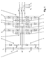
- Fig. 1 An embodiment of a three-phase converter circuit for switching three voltage levels is shown.
- the converter circuit after Fig. 1 has a DC voltage circuit 1, which is formed by a first capacitor C 1 and by a second capacitor C 2 connected in series with the first capacitor C 1 .
- the DC voltage circuit 1 has a first main terminal V + at the first capacitor C 1 , a second main terminal V- at the second capacitor C 2, and a partial terminal NP formed by the two series-connected capacitors C 1 , C 2 .
- a partial converter system 4 provided for each phase u, v, w, which is formed in each case by a first switch group 5, by a second switch group 6 and by a third switch group 7, each switch group 5, 6, 7 being formed by two series-connected power semiconductor switches is. Furthermore, in each partial converter system 4, the first switching group 5 is connected to the first main terminal V + and the second switching group 6 is connected to the second main terminal V-. Furthermore, the first switching group 5 is connected in series with the second switching group 6, wherein the connection point of the first switching group 5 with the second switching group 6 forms a phase connection.
- the third switching group 7, which is designed as a clamping switching group, is connected to the first Switching group 5, in particular with the connection point of the two series-connected power semiconductor switch of the first switching group 5, connected.
- the third switching group 7 is connected to the second switching group 6, in particular to the connection point of the two series-connected power semiconductor switches of the second switching group 6.
- the third switching group 7, in particular the connection point of the two series-connected power semiconductor switches of the third switching group 7, is connected to the partial connection NP.
- the power semiconductor switches of the first and second switching groups 5, 6 are according to Fig. 1 designed as controllable bidirectional power semiconductor switch, wherein the power semiconductor switches of the third switching group are formed as unidirectional non-controllable semiconductor switch.
- the power semiconductor switches of the third switching group are designed as controllable bidirectional power semiconductor switches.
- Fig. 1 is in the converter circuit commonly provided a first parallel to the first capacitor C 1 connected voltage reduction means 2.
- a second parallel to the second capacitor C 2 connected voltage reduction device 3 is provided.
- the first and second voltage reducing means 2, 3 are each formed by a resistor and a switch connected in series with the resistor, wherein and the first and second voltage reducing means 2, 3 is actuated by closing the associated switch.
- energy of the associated capacitor C 1 , C 2 is converted into heat in the associated resistor and thus the associated DC voltage U DC1 , U DC2 is reduced simply, quickly and effectively, so that the equalization of the two DC voltages U DC1 , U DC2 in desired mass.
- the actuation of the first and second voltage reduction means takes place in each case for a predetermined period of time. This period of time is preferably predetermined as a function of the thermal capacity of the resistor. The operation is carried out according to known to the expert criteria, which will not be discussed in detail at this point.
- each phase u, w, v of the converter circuit is connected to the first main terminal V + , to the second main terminal V or to the partial terminal NP by the power semiconductor switches after a predetermined sequence PM of switching states within a predetermined period of time, the switching states of Phases u, v, w are given to each other by switching state combinations SK.
- switching state combinations SK As already mentioned, is in Fig.
- FIG. 2a a state diagram of these switching state combinations SK, where "+" for a connection of the corresponding phase u, v, w with the first main terminal V + , "-" for a connection of the corresponding phase u, v, w with the second main terminal V- and "0" stands for a connection of the corresponding phase u, v, w with the partial connection NP and the lines between the switching state combinations SK represent permissible transitions between the switching state combinations SK.
- Fig. 2b are typical time courses of the phase output voltages U u , U v , U w of the converter circuit after Fig. 1 shown.
- phase output voltages U u , U v , U w are formed by the respective sequences PM of switching states, as an example in the phase output voltage U u for the phase U a sequence PM for the first half of the period of the phase output voltage U u is specially designated as the aforesaid predetermined period of time and a sequence PM for the second half of the period of the phase output voltage U u as the aforementioned predetermined time period.
- the phase output voltages U v , U w of the phase v and phase w are obtained according to Fig. 2b from the phase output voltage U u by a phase shift of 120 ° or 240 °.
- Such sequences are commonly referred to as so-called pulse patterns.
- the aforementioned DC voltage difference value becomes U NP monitored at a threshold value U DCS1 out, wherein when exceeding or falling below the threshold value U DCS1 the phases u, v, w after one of the switching state combinations SK depending on the previous switching state combination SK v the follow-up, the flow direction of a phase current i u , i v , i w and exceeding or falling below the threshold value U DCS1 selected switching state combination SK a with the first main terminal V + , be connected to the second main terminal V- or to the partial terminal NP.
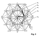
- FIG. 3 is a state diagram with switching state combinations SK of the phases of the converter circuit according to Fig. 2a and exemplified switching state combinations SK a , SK n , SK z1 , SK z2 according to the invention described in detail steps of the inventive method shown.
- an exemplary sequence 5 - 3 - 22 - 0 is based on switching state combinations SK, this sequence being followed by thick lines in the state diagram according to FIG Fig. 3 is specially marked.
- the switching combination 23 is selected according to the already mentioned dependencies as the selected switching state combination SK a , for example in the switching state combination 3, this transition, however, known undesirable large harmonics or change the fundamental of the phase output voltages U u , U v , U w generated and thus inadmissible, the phases u, v, w according to the invention in a general impermissible transition to the selected switching state combination SK a in a first step after a same phase conductor voltages U uv , U vw , U wu as the selected switching state combination SK a generating Switching state combination SK n with the first main terminal V + , connected to the second main terminal V- or to the partial connection NP.
- the phase conductor voltages U uv , u vw , u wu are the voltages that occur between the phase conductors (chained voltages).
- the switching state combination SK n generating the same phase conductor voltages U uv , U vw , U wu as the selected switching state combination SK a is the switching state combination SK n following the sequence of steps. According to Fig. 3 This switching state combination SK n following the sequence sequence is then, for example, the switching state combination 22, which follows the switching state combination 3.
- phase conductor voltages U uv , U vw , U wu are voltages between the phases u, v and v, w and w, u, respectively, the phase conductor voltages U uv , U vw , U wu for the sake of clarity in Fig. 1 are not shown.
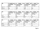
- All selected switching state combinations SK a are in a table according to Fig. 2c compiled. These switching state combinations SK a occur according to Fig. 2c and Fig. 3 in pairs, ie the paired switching state combinations SK a produce the same phase conductor voltages U uv , U vw , U wu .
- the phases u, v, w according to the invention according to a selected first additional switching state combination SK z1 and then in a third step after the selected switching state combination SK a with the first main terminal V + , with the second main terminal V- or with the partial connection NP connected.
- the first additional switching state combination SK z1 is the switching combination 18 and the selected switching state combination SK a the switching combination 23 already mentioned several times.
- the transitions according to the second step and according to the fourth step are specially marked by dashed thick lines.
- the first and the second additional switching state combination SK z1 , SK z2 are selected such that the per phase u, v, w from the first and second additional switching state combination SK z1 ; SK z2 corresponding phase output voltages U u, SK1 , U v, SKz1, U w, SKz1 , U u, SK2 , U v, SKz2 , U w, SKz2 averages formed U u , U v , U w are each equal to the u with respect to the phase, v, w corresponding phase output voltages U u, U v, U w of the same phase conductor voltages U uv, U vw, U wu as the selected switching state combination SK a generating switching
- t 1 is the contact time for the voltage U u
- SK1 and t 2 is the contact time for the voltage U u
- SK2 and t 1 t 2 .
- the time averages U v , U w for the phase v and the phase w result according to the above formula.
- the first step described above is advantageously achieved that no harmonics or change in the fundamental of the phase output voltages U u , U v , U w are generated, since the follow-up process is adhered to.
- the already explained second step is also required as a starting point for the transition to the selected switching state combinations SK a according to the third step.
- This above-described third step then advantageously has the effect that, for example, in the event of an asymmetry of the DC voltage circuit 1 occurring in the operating case of the converter circuit, ie if the first DC voltage U DC1 is greater than the second DC voltage U DC2 , the first DC voltage U DC1 is reduced in terms of amount , so that a magnitude adjustment is made to the second DC voltage U DC2 and thus a symmetrical distribution of the two DC voltages U DC1 , U DC2 of the DC voltage circuit 1 can be achieved.
- the selected switching state combinations SK a according to the third step and after Fig. 2c Inequalities in the amounts between the first and second DC voltage U DC1 , U DC2 are very specific, ie according to the case distinctions Fig.
- the selection of the first additional switching state combination SK z1 of the second step and the selection of the second additional switching state combination SK z2 of the fourth step advantageously serves to ensure the transition to the selected switching state combination SK a , ie to the third step, and the transition from the selected switching state combination SK a , ie from the third step, almost no significant harmonics or change the fundamental of the phase output voltages U u , U v , U w are generated at the same time as described above compensation of an occurring imbalance of the DC voltage circuit 1 by means of the selected switching state combination SK a .
- the phases u, v, w are preferably in the already mentioned fifth step Fig. 3 after the same phase conductor voltages U uv , U vw , U wu as the selected switching state combination SK a generating switching state combination SK n with the first main terminal V + , with the second main terminal V - or connected to the partial connection NP.
- Fig. 3 is that of the same phase conductor voltages U uv , U vw , U wu as the selected switching state combination SK a generating switching state combination SK n according to the fifth step then the switching state combination 22, so that through the fifth step back to the sequence sequence of the switching state combinations SK can be passed and the sequence sequence of the switching state combinations SK can be continued thereafter.
- the selected switching state combination SK a only a number of the phases u, v, w with the first main terminal V + and the remaining number of phases u, v, w with the sub-terminal NP or only a number of phases u, v, w with the second main terminal V and the remaining part of the phases u, v, w connected to the partial connection NP.
- the threshold value U DCS1 is preferably selected in the order of magnitude between 0% and 3% of the sum of the first and second DC voltage U DC1 , U DC2 , so that occurring inequalities in the amounts between the first and second DC voltage U DC1 , U DC2 by the above-mentioned process steps when exceeding and falling below the threshold value U DCS1 very early and thus can be compensated very quickly.
- the inventive improved method for balancing the DC circuit 1 of the converter circuit for switching three voltage levels is a very simple, efficient and therefore cost-effective solution, inequalities in the amounts of DC voltages U DC1 , U DC2 to the capacitors C 1 , C 2 of the DC circuit 1 without generating any significant harmonics or change in the fundamental oscillation of the phase output voltages U u , U v , U w to compensate.
Description
Die Erfindung bezieht sich auf das Gebiet der Leistungselektronik. Sie geht aus von einem Verfahren zur Symmetrierung eines Gleichspannungskreises einer Umrichterschaltung zur Schaltung von drei Spannungsniveaus gemäss dem Oberbegriff des unabhängigen Anspruchs.The invention relates to the field of power electronics. It is based on a method for balancing a DC voltage circuit of an inverter circuit for switching three voltage levels according to the preamble of the independent claim.
Heute werden in vielen Anwendungen Hochleistungsspannungsumrichter eingesetzt. Ein solcher Umrichter schaltet gängigerweise drei Spannungsniveaus, wozu ein Gleichspannungskreis vorgesehen ist, der durch einen ersten Kondensator und durch einen in Serie zum ersten Kondensator geschalteten zweiten Kondensator gebildet ist. Der Gleichspannungskreis weist weiterhin am ersten Kondensator einen ersten Hauptanschluss, am zweiten Kondensator einen zweiten Hauptanschluss und einen durch die zwei seriell miteinander verbundenen Kondensatoren gebildeten Teilanschluss auf. Weiterhin umfasst der Umrichter zur Schaltung von drei Spannungsniveaus Leistungshalbleiterschalter, welche in üblicher Weise verschaltet sind.Today high power voltage converters are used in many applications. Such a converter commonly switches three voltage levels, for which a DC voltage circuit is provided, which is formed by a first capacitor and by a second capacitor connected in series with the first capacitor. The DC voltage circuit furthermore has a first main connection on the first capacitor, a second main connection on the second capacitor, and a partial connection formed by the two capacitors connected in series with one another. Furthermore, the converter comprises the circuit of three voltage levels power semiconductor switch, which are connected in the usual way.
Während des Betriebs der Umrichterschaltung kann es nun vorkommen, dass entweder die am ersten Kondensator anliegende erste Gleichspannung grösser ist als die am zweiten Kondensator anliegende zweite Gleichspannung, oder dass die zweite Gleichspannung grösser ist als die erste Gleichspannung. Um dieser Unsymmetrie entgegenzuwirken, ist in dem Dokument
Ein weiteres Verfahren zur Symmetrierung eines Gleichspannungskreises eines Umrichterschaltung zur Schaltung von drei Spannungsniveaus ist in dem Dokument
In einem in
Darüber hinaus wird der vorstehend genannte Gleichspannungsdifferenzwert auf einen Schwellwert hin überwacht, wobei bei Überschreiten des Schwellwertes, d.h. falls die erste Gleichspannung grösser ist als die zweite Gleichspannung, oder bei Unterschreiten des Schwellwertes, d.h. falls die zweite Gleichspannung grösser ist als die erste Gleichspannung, die drei Phasen nach einer aus den Schaltzustandskombinationen ausgewählten Schaltzu-standskombination mit dem ersten Hauptanschluss, mit dem zweiten Hauptanschluss oder mit dem Teilanschluss verbunden werden. Die Auswahl der geeigneten Schaltzustandskombination erfolgt in Abhängigkeit der vorangehenden Schaltzustandskombination des Abfolgeablaufs, der Flussrichtung eines Phasenstromes und des Überschreitens oder des Unterschreitens des Schwellwertes. Durch die vorstehend beschriebene Verbindung der drei Phasen mit dem ersten Hauptanschluss, mit dem zweiten Hauptanschluss oder mit dem Teilanschluss wird erreicht, dass beispielsweise bei einer auftretenden Unsymmetrie des Gleichspannungskreises im Betriebsfall der Umrichterschaltung, d.h. falls zum Beispiel die erste Gleichspannung betragsmässig grösser als die zweite Gleichspannung ist, die erste Gleichspannung betragsmässig verringert wird, so dass eine betragsmässige Angleichung an die zweite Gleichspannung erfolgt und somit eine symmetrische Verteilung der beiden Gleichspannungen des Gleichspannungskreises erzielt werden kann.In addition, the above-mentioned DC voltage difference value is monitored for a threshold value, wherein when the threshold value is exceeded, ie if the first DC voltage is greater than the second DC voltage, or falls below the threshold value, ie if the second DC voltage is greater than the first DC voltage, the three phases according to a Schaltzu-stand combination selected from the switching state combinations be connected to the first main connection, to the second main connection or to the partial connection. The selection of the appropriate switching state combination takes place as a function of the preceding switching state combination of the sequence sequence, the flow direction of a phase current and the exceeding or undershooting of the threshold value. By means of the above-described connection of the three phases to the first main connection, to the second main connection or to the partial connection, it is achieved that, for example, in the event of an asymmetry of the DC voltage circuit occurring in the case of operation of the converter circuit, ie if, for example, the first DC voltage is greater in magnitude than the second DC voltage is, the first DC voltage is reduced in terms of amount, so that a magnitude adjustment is made to the second DC voltage and thus a symmetrical distribution of the two DC voltages of the DC voltage circuit can be achieved.
In dem in Dokument
Aufgabe der Erfindung ist es deshalb, ein verbessertes Verfahren zur Symmetrierung eines Gleichspannungskreises einer Umrichterschaltung zur Schaltung von drei Spannungsniveaus anzugeben, durch welches Ungleichheiten in den Beträgen von Gleichspannungen an Kondensatoren des Gleichspannungskreises in einfacher Weise und ohne nennenswerte Erzeugung von Oberschwingungen beziehungsweise Änderung der Grundschwingung der Phasenausgangsspannungen der Umrichterschaltung kompensiert werden können. Diese Aufgabe wird durch die Merkmale des Anspruchs 1 gelöst. In den abhängigen Ansprüchen sind vorteilhafte Weiterbildungen der Erfindung angegeben.The object of the invention is therefore an improved method for balancing a DC voltage circuit of a converter circuit for switching three voltage levels specify by which inequalities in the amounts of DC voltages across capacitors of the DC circuit in a simple manner and without significant generation of harmonics or change the fundamental of the phase output voltages of the converter circuit can be compensated. This object is solved by the features of claim 1. In the dependent claims advantageous developments of the invention are given.
Beim erfindungsgemässen Verfahren zur Symmetrierung eines Gleichspannungskreises einer Umrichterschaltung zur Schaltung von drei Spannungsniveaus ist der Gleichspannungskreis durch einen ersten Kondensator und durch einen in Serie zum ersten Kondensator geschalteten zweiten Kondensator gebildet und weist weiterhin am ersten Kondensator einen ersten Hauptanschluss, am zweiten Kondensator einen zweiten Hauptanschluss und einen durch die zwei seriell verbundenen Kondensatoren gebildeten Teilanschluss auf, wobei aus einer am ersten Kondensator anliegenden ersten Gleichspannung und aus einer am zweiten Kondensator anliegenden zweiten Gleichspannung ein Gleichspannungsdifferenzwert gebildet wird. Ferner wird jede Phase der Umrichterschaltung durch Leistungshalbleiterschalter der Umrichterschaltung nach jeweils einer vorgegebenen Abfolge von Schaltzuständen innerhalb einer vorgegebenen Zeitdauer mit dem ersten Hauptanschluss, mit dem zweiten Hauptanschluss oder mit dem Teilanschluss verbunden, wobei die Schaltzustände der Phasen zueinander durch Schaltzustandskombinationen vorgegeben sind. Die Schaltzustandskombinationen sind weiterhin in einem Abfolgeablauf festgelegt. Darüber hinaus wird der Gleichspannungsdifferenzwert auf einen Schwellwert hin überwacht wird, wobei bei Überschreiten oder Unterschreiten des Schwellwertes die Phasen nach einer aus den Schaltzustandskombinationen in Abhängigkeit der vorangehenden Schaltzustandskombination des Abfolgeablaufs, der Flussrichtung eines Phasenstromes und des Überschreitens oder des Unterschreitens des Schwellwertes ausgewählten Schaltzustandskombination mit dem ersten Hauptanschluss, mit dem zweiten Hauptanschluss oder mit dem Teilanschluss verbunden werden.In the method according to the invention for balancing a DC voltage circuit of a converter circuit for switching three voltage levels, the DC voltage circuit is formed by a first capacitor and by a second capacitor connected in series with the first capacitor and furthermore has a first main connection on the first capacitor, a second main connection on the second capacitor a partial connection formed by the two capacitors connected in series, wherein a DC voltage difference value is formed from a first DC voltage applied to the first capacitor and from a second DC voltage applied to the second capacitor. Furthermore, each phase of the converter circuit is connected by power semiconductor switch of the converter circuit after each predetermined sequence of switching states within a predetermined period of time with the first main terminal, with the second main terminal or with the partial terminal, the switching states of the phases are given to each other by switching state combinations. The switching state combinations are still set in a sequence. In addition, the DC voltage difference value is monitored for a threshold value, wherein when exceeding or falling below the threshold value, the phases according to a selected from the switching state combinations depending on the preceding switching state combination of the sequence sequence, the flow direction of a phase current and the exceeding or falling below the threshold switching state combination with the first main connection, to the second main connection or to the partial connection.
Erfindungsgemäss werden die Phasen bei einem unzulässigen Übergang zur ausgewählten Schaltzustandskombination, d.h. einem die Grundschwingung von Phasenausgangsspannungen ändernden Übergang, in einem ersten Schritt nach einer dieselben Phasenleiterspannungen wie die ausgewählte Schaltzustandskombination erzeugende Schaltzustandskombination mit dem ersten Hauptanschluss, mit dem zweiten Hauptanschluss oder mit dem Teilanschluss verbunden, wobei die dieselben Phasenleiterspannungen wie die ausgewählte Schaltzustandskombination erzeugende Schaltzustandskombination die im Abfolgeablauf nächstfolgende Schaltzustandskombination ist. Ferner werden die Phasen in einem zweiten Schritt nach einer gewählten ersten zusätzlichen Schaltzustandskombination und danach in einem dritten Schritt nach der ausgewählten Schaltzustandskombination mit dem ersten Hauptanschluss, mit dem zweiten Hauptanschluss oder mit dem Teilanschluss verbunden. In einem vierten Schritt werden dann die Phasen nach einer gewählten zweiten zusätzlichen Schaltzustandskombination mit dem ersten Hauptanschluss, mit dem zweiten Hauptanschluss oder mit dem Teilanschluss verbunden, wobei die erste und die zweite zusätzliche Schaltzustandskombination derart gewählt werden, dass die je Phase aus den der ersten und zweiten zusätzlichen Schaltzustandskombination entsprechenden Phasenausgangsspannungen gebildeten Mittelwerte jeweils gleich den in Bezug auf die Phase entsprechenden Phasenausgangsspannungen der dieselben Phasenleiterspannungen wie die ausgewählte Schaltzustandskombination erzeugende Schaltzustandskombination sind.According to the invention, the phases are connected to the first main connection, to the second main connection or to the partial connection in an impermissible transition to the selected switching state combination, ie a transition changing the fundamental of phase output voltages, in a first step after a switching state combination generating the same phase conductor voltages as the selected switching state combination, the same phase conductor voltages as the one selected Switching state combination generating switching state combination is the next in the sequence sequence switching state combination. Furthermore, in a second step, the phases are connected after a selected first additional switching state combination and then in a third step according to the selected switching state combination to the first main connection, to the second main connection or to the partial connection. In a fourth step, the phases are then connected to the first main connection, to the second main connection or to the partial connection according to a selected second additional switching state combination, wherein the first and the second additional switching state combination are selected such that the respective phase of the first and second averaging values corresponding respectively to the phase corresponding to the phase output voltages of the same phase conductor voltages as the selected switching state combination generating switching state combination are second auxiliary switching state combination of corresponding phase output voltages.
Mittels der vorstehend genannten erfindungsgemässen Schritte eins bis vier wird vorteilhaft erreicht, dass Ungleichheiten in den Beträgen von Gleichspannungen an Kondensatoren des Gleichspannungskreises in einfacher Weise kompensiert werden, wobei gleichzeitig nahezu keine nennenswerten Oberschwingungen beziehungsweise Änderung der Grundschwingung der Phasenausgangsspannungen der Umrichterschaltung erzeugt werden. Die Qualität der Phasenausgangsspannungen kann durch das erfindungsgemässe Verfahren somit entscheidend verbessert werden.By means of the abovementioned steps one to four according to the invention, it is advantageously achieved that inequalities in the amounts of DC voltages on capacitors of the DC voltage circuit are compensated in a simple manner, wherein at the same time virtually no appreciable harmonics or change in the fundamental frequency of the phase output voltages of the converter circuit are generated. The quality of the phase output voltages can thus be decisively improved by the method according to the invention.
Diese und weitere Aufgaben, Vorteile und Merkmale der vorliegenden Erfindung werden aus der nachfolgenden detaillierten Beschreibung bevorzugter Ausführungsformen der Erfindung in Verbindung mit der Zeichnung offensichtlich.These and other objects, advantages and features of the present invention will become more apparent from the following detailed description of preferred embodiments of the invention taken in conjunction with the accompanying drawings.
Es zeigen:
- Fig. 1
- eine Ausführungsform einer dreiphasigen Umrichterschaltung zur Schaltung von drei Spannungsniveaus,
- Fig. 2a
- ein Zustandsdiagramm mit Schaltzustandkombinationen der Phasen der Umrichterschaltung,
- Fig. 2b
- typische Zeitverläufe der Phasenausgangsspannungen der Umrichterschaltung nach
Fig. 1 , - Fig. 2c
- eine Tabelle mit aus
Fig. 2a ausgewählten Schaltzustandskombinationen und - Fig. 3
- ein Zustandsdiagramm mit Schaltzustandkombinationen der Phasen der Umrichterschaltung gemäss
Fig. 2a und beispielhaft hervorgehobenen Schaltzustandkombinationen entsprechend den erfindungsgemässen Schritten des erfindungsgemässen Verfahrens.
- Fig. 1
- an embodiment of a three-phase converter circuit for switching three voltage levels,
- Fig. 2a
- a state diagram with switching state combinations of the phases of the converter circuit,
- Fig. 2b
- typical time courses of the phase output voltages of the converter circuit after
Fig. 1 . - Fig. 2c
- a table with
Fig. 2a selected switching state combinations and - Fig. 3
- a state diagram with switching state combinations of the phases of the converter circuit according to
Fig. 2a and exemplified switching state combinations according to the inventive steps of the inventive method.
Die in der Zeichnung verwendeten Bezugszeichen und deren Bedeutung sind in der Bezugszeichenliste zusammengefasst aufgelistet. Grundsätzlich sind in den Figuren gleiche Teile mit gleichen Bezugszeichen versehen. Die beschriebenen Ausführungsformen stehen beispielhaft für den Erfindungsgegenstand und haben keine beschränkende Wirkung.The reference numerals used in the drawings and their meaning are listed in the list of reference numerals. Basically, the same parts are provided with the same reference numerals in the figures. The described embodiments are exemplary of the subject invention and have no limiting effect.
In
Es wird nun aus einer am ersten Kondensator C1 anliegenden ersten Gleichspannung UDC1 und aus einer am zweiten Kondensator C2 anliegenden zweiten Gleichspannung UDC2 ein Gleichspannungsdifferenzwert 
Ferner wird jede Phase u, w, v der Umrichterschaltung durch die Leistungshalbleiterschalter nach jeweils einer vorgegebenen Abfolge PM von Schaltzuständen innerhalb einer vorgegebenen Zeitdauer mit dem ersten Hauptanschluss V+, mit dem zweiten Hauptanschluss V. oder mit dem Teilanschluss NP verbunden, wobei die Schaltzustände der Phasen u, v, w zueinander durch Schaltzustandskombinationen SK vorgegeben sind. Wie bereits eingangs erwähnt, ist in
In
In einem zweiten Schritt werden die Phasen u, v, w erfindungsgemäss nach einer gewählten ersten zusätzlichen Schaltzustandskombination SKz1 und danach in einem dritten Schritt nach der ausgewählten Schaltzustandskombination SKa mit dem ersten Hauptanschluss V+, mit dem zweiten Hauptanschluss V- oder mit dem Teilanschluss NP verbunden. Gemäss 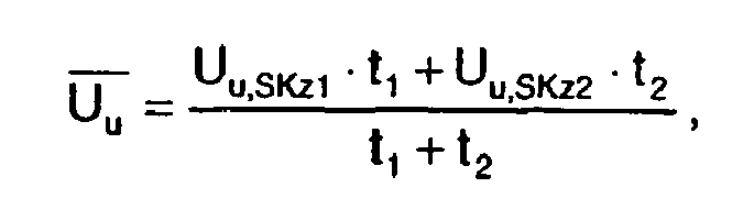
wobei t1 die Anliegezeit für die Spannung Uu,SK1 und t2 die Anliegezeit für die Spannung Uu,SK2 ist und t1=t2 ist. Die zeitlichen Mittelwerte
where t 1 is the contact time for the voltage U u, SK1 and t 2 is the contact time for the voltage U u, SK2 and t 1 = t 2 . The time averages
Durch den vorstehend beschriebenen ersten Schritt wird vorteilhaft erreicht, dass keine Oberschwingungen beziehungsweise Änderung der Grundschwingung der Phasenausgangsspannungen Uu, Uv, Uw erzeugt werden, da beim der Abfolgeablauf einhalten wird. Der bereits erläuterte zweite Schritts wird ferner als Ausgangspunkt für den Übergang zur ausgewählten Schaltzustandskombinationen SKa gemäss dem dritten Schritt benötigt. Dieser vorstehend beschriebe dritte Schritt bewirkt dann vorteilhaft, dass beispielsweise bei einer auftretenden Unsymmetrie des Gleichspannungskreises 1 im Betriebsfall der Umrichterschaltung, d.h. falls zum Beispiel die ersten Gleichspannung UDC1 betragsmässig grösser als die zweite Gleichspannung UDC2 ist, die erste Gleichspannung UDC1 betragsmässig verringert wird, so dass eine betragsmässige Angleichung an die zweite Gleichspannung UDC2 erfolgt und somit eine symmetrische Verteilung der beiden Gleichspannungen UDC1, UDC2 des Gleichspannungskreis 1 erzielt werden kann. Mittels der ausgewählten Schaltzustandskombinationen SKa gemäss dem dritten Schritt und nach
Die Phasen u, v, w werden vorzugsweise in dem bereits erwähnten fünften Schritt gemäss
Vorzugsweise wird bei der ausgewählten Schaltzustandskombination SKa nur eine Anzahl der Phasen u, v, w mit dem ersten Hauptanschluss V+ und die restliche Anzahl der Phasen u, v, w mit dem Teilanschluss NP oder nur eine Anzahl der Phasen u, v, w mit dem zweiten Hauptanschluss V- und der restliche Teil der Phasen u, v, w mit dem Teilanschluss NP verbunden.Preferably, in the selected switching state combination SK a only a number of the phases u, v, w with the first main terminal V + and the remaining number of phases u, v, w with the sub-terminal NP or only a number of phases u, v, w with the second main terminal V and the remaining part of the phases u, v, w connected to the partial connection NP.
Desweiteren wird der Schwellwert UDCS1 vorzugsweise in der Grössenordnung zwischen 0% und 3% der Summe der ersten und zweiten Gleichspannung UDC1, UDC2 gewählt, so dass auftretende Ungleichheiten in den Beträgen zwischen der ersten und zweiten Gleichspannung UDC1, UDC2 durch die vorstehend genannten Verfahrensschritte bei Überschreiten und Unterschreiten des Schwellwertes UDCS1 sehr frühzeitig und damit sehr schnell ausgeglichen werden können.Furthermore, the threshold value U DCS1 is preferably selected in the order of magnitude between 0% and 3% of the sum of the first and second DC voltage U DC1 , U DC2 , so that occurring inequalities in the amounts between the first and second DC voltage U DC1 , U DC2 by the above-mentioned process steps when exceeding and falling below the threshold value U DCS1 very early and thus can be compensated very quickly.
Insgesamt stellt das erfindungsgemässe verbesserte Verfahren zur Symmetrierung des Gleichspannungskreises 1 der Umrichterschaltung zur Schaltung von drei Spannungsniveaus eine sehr einfache, effiziente und somit kostengünstige Lösung dar, Ungleichheiten in den Beträgen der Gleichspannungen UDC1, UDC2 an den Kondensatoren C1, C2 des Gleichspannungskreises 1 ohne Erzeugung nennenswerter Oberschwingungen beziehungsweise Änderung der Grundschwingung der Phasenausgangsspannungen Uu, Uv, Uw zu kompensieren.Overall, the inventive improved method for balancing the DC circuit 1 of the converter circuit for switching three voltage levels is a very simple, efficient and therefore cost-effective solution, inequalities in the amounts of DC voltages U DC1 , U DC2 to the capacitors C 1 , C 2 of the DC circuit 1 without generating any significant harmonics or change in the fundamental oscillation of the phase output voltages U u , U v , U w to compensate.
- 11
- GleichspannungskreisDC circuit
- 22
- erste Spannungsreduziereinrichtungfirst voltage reduction device
- 33
- zweite Spannungsreduziereinrichtungsecond voltage reduction device
- 44
- Teilumrichtersystemconverter subsystem
- 55
- erste Schaltgruppefirst switching group
- 66
- zweite Schaltgruppesecond switching group
- 77
- dritte Schaltgruppethird switching group
Claims (4)
- Method for balancing a DC voltage circuit (1) in a converter circuit for switching three voltage levels, in which the DC voltage circuit (1) is formed by a first capacitor (C1) and by a second capacitor (C2) which is connected in series with the first capacitor (C1) and has a first main connection (V+) on the first capacitor (C1), a second main connection (V-) on the second capacitor (C2), and a partial connection (NP) which is formed by the two series-connected capacitors (C1, C2), and a DC voltage difference value (
UNP ) is formed from the DC voltages (UDC1, UDC2) across the capacitors (C1, C2), in which
each phase (u,v,w) of the converter circuit is connected by means of power semiconductor switches in the converter circuit, in each case after a predetermined sequence (PM) of switching states within a predetermined time period, to the first main connection (V+), to the second main connection (V-) or to the partial connection (NP), with the switching states of the phases (u,v,w) with respect to one another being predetermined by switching state combinations (SK), and with the switching state combinations (SK) being defined in a sequence,
in which the DC voltage difference value (UNP ) is monitored for a threshold value (UDCS1), and
in which, if the threshold value (UDCS1) is overshot or undershot on the basis of a switching state combination (SKa) which is selected as a function of the previous switching state combinations (SKV) in the sequence, the flow direction of a phase current (iu, iv, iw) and the overshooting or the undershooting of the threshold (UDCS1), the phases (u,v,w) are connected to the first main connection (V+), to the second main connection (V-) or to the partial connection (NP),
characterized
in that, when a transition into the selected switching state combination (SKa) which changes the fundamental frequency of the phase output voltages (Uu, Uv, Uw) takes place, in a first step after a switching state combination (SKn) which produces the same phase conductor voltages (Uuv, Uvw, Uwu) as the selected switching state combination (SKa), the phases (u, v, w) are connected to the first main connection (V+), to the second main connection (V-) or to the partial connection (NP), with the switching state combination (SKn) which produces the same phase conductor voltages (Uuv, Uvw, Uwu) as the selected switching state combination (SKa) being the next switching state combination (SKn) in the sequence,
in that, in a second state after a selected first additional switching state combination (SKz1) and, after this, in a third step after the selected switching state combination (SKa), the phases (u, v, w) are connected to the first main connection (V+), to the second main connection (V-) or to the partial connection (NP), and
in that in a fourth step after a selected second additional switching state combination (SKz2), the phases (u,v,w) are connected to the first main connection (V+), to the second main connection (V-) or to the partial connection (NP), with the first and the second additional switching state combinations (SKz1; SKz2) being selected such that the mean values (U u,U v,U w) formed from each phase (u,v,w) from the phase output voltages (Uu,SK1, Uv,SKz1, Uw,SKz1, Uu,SK2, Uv,SKz2, Uw,SKz2) which correspond to the first and the second additional switching state combination to (SKz1; SKz2) in each case being equal to the phase output voltages (Uu, Uv, Uw) which correspond with respect to the phase (u, v, w) of the same phase conductor voltages (Uuv, Uvw, Uwu) as the switching state combination (SKn) which produces the selected switching state combination (SKa). - Method according to Claim 1, characterized in that, in a fifth step after the switching state combination (SKn) which produces the same phase conductor voltages (Uuv, Uvw, Uwu) as the selected switching state combination (SKa), the phases (u,v,w) are connected to the first main connection (V+), to the second connection (V-) or to the partial connection (NP).
- Method according to one of the preceding claims, characterized in that, in the selected switching state combination (SKa), only a number of the phases (u,v,w) are connected to the first main connection (V+), and the remaining number of the phases (u,v,w) are connected to the partial connection (NP), or only a number of the phases (u,v,w) are connected to the second main connection (V-), and the remaining phases (u,v,w) are connected to the partial connection (NP).
- Method according to one of the preceding claims, characterized in that the threshold value (UDCS1) is chosen to be in the order of magnitude of between 0% and 3% of the sum of the first and the second DC voltage (UDC1, UDC2).
Priority Applications (1)
| Application Number | Priority Date | Filing Date | Title |
|---|---|---|---|
| EP20040405509 EP1544994B1 (en) | 2003-12-15 | 2004-08-13 | Improved method for balancing the DC link of a three level inverter |
Applications Claiming Priority (3)
| Application Number | Priority Date | Filing Date | Title |
|---|---|---|---|
| EP03405895 | 2003-12-15 | ||
| EP03405895 | 2003-12-15 | ||
| EP20040405509 EP1544994B1 (en) | 2003-12-15 | 2004-08-13 | Improved method for balancing the DC link of a three level inverter |
Publications (3)
| Publication Number | Publication Date |
|---|---|
| EP1544994A2 EP1544994A2 (en) | 2005-06-22 |
| EP1544994A3 EP1544994A3 (en) | 2007-04-11 |
| EP1544994B1 true EP1544994B1 (en) | 2008-05-28 |
Family
ID=34524783
Family Applications (1)
| Application Number | Title | Priority Date | Filing Date |
|---|---|---|---|
| EP20040405509 Not-in-force EP1544994B1 (en) | 2003-12-15 | 2004-08-13 | Improved method for balancing the DC link of a three level inverter |
Country Status (1)
| Country | Link |
|---|---|
| EP (1) | EP1544994B1 (en) |
Families Citing this family (3)
| Publication number | Priority date | Publication date | Assignee | Title |
|---|---|---|---|---|
| FR2947971A1 (en) | 2009-07-07 | 2011-01-14 | Converteam Technology Ltd | DEVICE FOR CONVERTING A CONTINUOUS VOLTAGE OF INPUT INTO AN ALTERNATIVE OUTPUT VOLTAGE, AND METHOD FOR CONTROLLING A SWITCH OF SUCH A DEVICE |
| EP2413489B1 (en) | 2010-07-30 | 2013-09-11 | Vinotech Holdings S.à.r.l. | Highly efficient half-bridge DC/AC converter |
| CN105226982B (en) * | 2015-11-02 | 2018-01-12 | 南京航空航天大学 | A kind of three level NPC inverter midpoint potential balance control methods based on midpoint electric current |
Family Cites Families (4)
| Publication number | Priority date | Publication date | Assignee | Title |
|---|---|---|---|---|
| DE3875728D1 (en) * | 1988-08-30 | 1992-12-10 | Siemens Ag | METHOD FOR OPERATING A THREE-POINT INVERTER. |
| JP2526700B2 (en) * | 1990-04-11 | 1996-08-21 | 三菱電機株式会社 | 3-phase 3-value level inverter |
| CN100492856C (en) * | 1999-08-12 | 2009-05-27 | 株式会社安川电机 | Tri-phase neutral point clamping type PWM inventer device |
| JP3434746B2 (en) * | 1999-09-01 | 2003-08-11 | 芝府エンジニアリング株式会社 | Control device for power converter |
-
2004
- 2004-08-13 EP EP20040405509 patent/EP1544994B1/en not_active Not-in-force
Also Published As
| Publication number | Publication date |
|---|---|
| EP1544994A2 (en) | 2005-06-22 |
| EP1544994A3 (en) | 2007-04-11 |
Similar Documents
| Publication | Publication Date | Title |
|---|---|---|
| EP3496259B1 (en) | Electrical converter system | |
| EP1759450B1 (en) | Low harmonic multiphase converter circuit | |
| EP1695434B1 (en) | Converter circuit with two partial converters | |
| EP3245727B1 (en) | Converter module for a multi-level energy converter | |
| EP2348627A1 (en) | Converter circuit and method for operating a multilevel converter circuit | |
| DE112008004182T5 (en) | Magnetic energy recovery switch, comprising a protection circuit | |
| EP1670135B1 (en) | Method of operating a rotary electrical machine | |
| DE2846491A1 (en) | DEVICE AND METHOD FOR GENERATING ELECTRICAL SIGNALS | |
| EP2110939A1 (en) | Inverter and method for controlling an inverter with flying capacitors | |
| EP2223426B1 (en) | Method for operating a rotating electric machine | |
| EP1513249B1 (en) | Method for neutral-point balancing of a three-level inverter | |
| EP2034606B1 (en) | Method for operating an electric rotary machine | |
| EP3602762B1 (en) | Inverter | |
| EP1544994B1 (en) | Improved method for balancing the DC link of a three level inverter | |
| EP3895312B1 (en) | Electronic switch with power regulation | |
| DE102016118039A1 (en) | Solar module, photovoltaic system and voltage limiting method | |
| EP3326283B1 (en) | Method for operating an inverter, inverter, and photovoltaic system | |
| DE102019105196B4 (en) | Method for current limitation in the event of transient voltage changes at an AC output of a multilevel inverter and multilevel inverter | |
| EP2182625B1 (en) | Method for operating a frequency converter, computer program to implement such a method and data medium and computer system, especially frequency converter on which such a computer program is saved or loaded | |
| DE10320521B4 (en) | Electrical control device for controls and method for controlling controls | |
| EP4254767A1 (en) | Method and system for modifying carrier signals in phase shifted pulse width modulation | |
| EP2893603A2 (en) | Method for driving an active bridge rectifier in the event of load shedding, rectifier arrangement and computer program product | |
| EP1298781B1 (en) | Power converter device and method for adjusting a variable DC voltage | |
| EP1988402A2 (en) | Method for determining work/power | |
| EP1742343A1 (en) | Modulation method |
Legal Events
| Date | Code | Title | Description |
|---|---|---|---|
| PUAI | Public reference made under article 153(3) epc to a published international application that has entered the european phase |
Free format text: ORIGINAL CODE: 0009012 |
|
| AK | Designated contracting states |
Kind code of ref document: A2 Designated state(s): AT BE BG CH CY CZ DE DK EE ES FI FR GB GR HU IE IT LI LU MC NL PL PT RO SE SI SK TR |
|
| AX | Request for extension of the european patent |
Extension state: AL HR LT LV MK |
|
| PUAL | Search report despatched |
Free format text: ORIGINAL CODE: 0009013 |
|
| AK | Designated contracting states |
Kind code of ref document: A3 Designated state(s): AT BE BG CH CY CZ DE DK EE ES FI FR GB GR HU IE IT LI LU MC NL PL PT RO SE SI SK TR |
|
| AX | Request for extension of the european patent |
Extension state: AL HR LT LV MK |
|
| 17P | Request for examination filed |
Effective date: 20070430 |
|
| AKX | Designation fees paid |
Designated state(s): AT BE BG CH CY CZ DE DK EE ES FI FR GB GR HU IE IT LI LU MC NL PL PT RO SE SI SK TR |
|
| GRAP | Despatch of communication of intention to grant a patent |
Free format text: ORIGINAL CODE: EPIDOSNIGR1 |
|
| GRAS | Grant fee paid |
Free format text: ORIGINAL CODE: EPIDOSNIGR3 |
|
| GRAA | (expected) grant |
Free format text: ORIGINAL CODE: 0009210 |
|
| AK | Designated contracting states |
Kind code of ref document: B1 Designated state(s): AT BE BG CH CY CZ DE DK EE ES FI FR GB GR HU IE IT LI LU MC NL PL PT RO SE SI SK TR |
|
| REG | Reference to a national code |
Ref country code: GB Ref legal event code: FG4D Free format text: NOT ENGLISH |
|
| REG | Reference to a national code |
Ref country code: CH Ref legal event code: EP |
|
| REF | Corresponds to: |
Ref document number: 502004007272 Country of ref document: DE Date of ref document: 20080710 Kind code of ref document: P |
|
| REG | Reference to a national code |
Ref country code: CH Ref legal event code: NV Representative=s name: ABB SCHWEIZ AG INTELLECTUAL PROPERTY (CH-LC/IP) |
|
| REG | Reference to a national code |
Ref country code: IE Ref legal event code: FG4D Free format text: LANGUAGE OF EP DOCUMENT: GERMAN |
|
| PG25 | Lapsed in a contracting state [announced via postgrant information from national office to epo] |
Ref country code: SI Free format text: LAPSE BECAUSE OF FAILURE TO SUBMIT A TRANSLATION OF THE DESCRIPTION OR TO PAY THE FEE WITHIN THE PRESCRIBED TIME-LIMIT Effective date: 20080528 |
|
| PG25 | Lapsed in a contracting state [announced via postgrant information from national office to epo] |
Ref country code: ES Free format text: LAPSE BECAUSE OF FAILURE TO SUBMIT A TRANSLATION OF THE DESCRIPTION OR TO PAY THE FEE WITHIN THE PRESCRIBED TIME-LIMIT Effective date: 20080908 Ref country code: FI Free format text: LAPSE BECAUSE OF FAILURE TO SUBMIT A TRANSLATION OF THE DESCRIPTION OR TO PAY THE FEE WITHIN THE PRESCRIBED TIME-LIMIT Effective date: 20080528 |
|
| PG25 | Lapsed in a contracting state [announced via postgrant information from national office to epo] |
Ref country code: NL Free format text: LAPSE BECAUSE OF FAILURE TO SUBMIT A TRANSLATION OF THE DESCRIPTION OR TO PAY THE FEE WITHIN THE PRESCRIBED TIME-LIMIT Effective date: 20080528 |
|
| NLV1 | Nl: lapsed or annulled due to failure to fulfill the requirements of art. 29p and 29m of the patents act | ||
| REG | Reference to a national code |
Ref country code: IE Ref legal event code: FD4D |
|
| PG25 | Lapsed in a contracting state [announced via postgrant information from national office to epo] |
Ref country code: CZ Free format text: LAPSE BECAUSE OF FAILURE TO SUBMIT A TRANSLATION OF THE DESCRIPTION OR TO PAY THE FEE WITHIN THE PRESCRIBED TIME-LIMIT Effective date: 20080528 Ref country code: IE Free format text: LAPSE BECAUSE OF FAILURE TO SUBMIT A TRANSLATION OF THE DESCRIPTION OR TO PAY THE FEE WITHIN THE PRESCRIBED TIME-LIMIT Effective date: 20080528 Ref country code: DK Free format text: LAPSE BECAUSE OF FAILURE TO SUBMIT A TRANSLATION OF THE DESCRIPTION OR TO PAY THE FEE WITHIN THE PRESCRIBED TIME-LIMIT Effective date: 20080528 Ref country code: PT Free format text: LAPSE BECAUSE OF FAILURE TO SUBMIT A TRANSLATION OF THE DESCRIPTION OR TO PAY THE FEE WITHIN THE PRESCRIBED TIME-LIMIT Effective date: 20081028 Ref country code: SE Free format text: LAPSE BECAUSE OF FAILURE TO SUBMIT A TRANSLATION OF THE DESCRIPTION OR TO PAY THE FEE WITHIN THE PRESCRIBED TIME-LIMIT Effective date: 20080828 |
|
| PG25 | Lapsed in a contracting state [announced via postgrant information from national office to epo] |
Ref country code: SK Free format text: LAPSE BECAUSE OF FAILURE TO SUBMIT A TRANSLATION OF THE DESCRIPTION OR TO PAY THE FEE WITHIN THE PRESCRIBED TIME-LIMIT Effective date: 20080528 Ref country code: RO Free format text: LAPSE BECAUSE OF FAILURE TO SUBMIT A TRANSLATION OF THE DESCRIPTION OR TO PAY THE FEE WITHIN THE PRESCRIBED TIME-LIMIT Effective date: 20080528 |
|
| PG25 | Lapsed in a contracting state [announced via postgrant information from national office to epo] |
Ref country code: MC Free format text: LAPSE BECAUSE OF NON-PAYMENT OF DUE FEES Effective date: 20080831 |
|
| PLBE | No opposition filed within time limit |
Free format text: ORIGINAL CODE: 0009261 |
|
| STAA | Information on the status of an ep patent application or granted ep patent |
Free format text: STATUS: NO OPPOSITION FILED WITHIN TIME LIMIT |
|
| PG25 | Lapsed in a contracting state [announced via postgrant information from national office to epo] |
Ref country code: EE Free format text: LAPSE BECAUSE OF FAILURE TO SUBMIT A TRANSLATION OF THE DESCRIPTION OR TO PAY THE FEE WITHIN THE PRESCRIBED TIME-LIMIT Effective date: 20080528 Ref country code: BG Free format text: LAPSE BECAUSE OF FAILURE TO SUBMIT A TRANSLATION OF THE DESCRIPTION OR TO PAY THE FEE WITHIN THE PRESCRIBED TIME-LIMIT Effective date: 20080828 |
|
| 26N | No opposition filed |
Effective date: 20090303 |
|
| PG25 | Lapsed in a contracting state [announced via postgrant information from national office to epo] |
Ref country code: BE Free format text: LAPSE BECAUSE OF NON-PAYMENT OF DUE FEES Effective date: 20080831 |
|
| PG25 | Lapsed in a contracting state [announced via postgrant information from national office to epo] |
Ref country code: AT Free format text: LAPSE BECAUSE OF NON-PAYMENT OF DUE FEES Effective date: 20080813 |
|
| PGFP | Annual fee paid to national office [announced via postgrant information from national office to epo] |
Ref country code: CH Payment date: 20090825 Year of fee payment: 6 Ref country code: DE Payment date: 20090821 Year of fee payment: 6 Ref country code: GB Payment date: 20090827 Year of fee payment: 6 |
|
| PGFP | Annual fee paid to national office [announced via postgrant information from national office to epo] |
Ref country code: IT Payment date: 20090819 Year of fee payment: 6 |
|
| PG25 | Lapsed in a contracting state [announced via postgrant information from national office to epo] |
Ref country code: PL Free format text: LAPSE BECAUSE OF FAILURE TO SUBMIT A TRANSLATION OF THE DESCRIPTION OR TO PAY THE FEE WITHIN THE PRESCRIBED TIME-LIMIT Effective date: 20080528 |
|
| PG25 | Lapsed in a contracting state [announced via postgrant information from national office to epo] |
Ref country code: CY Free format text: LAPSE BECAUSE OF FAILURE TO SUBMIT A TRANSLATION OF THE DESCRIPTION OR TO PAY THE FEE WITHIN THE PRESCRIBED TIME-LIMIT Effective date: 20080528 Ref country code: HU Free format text: LAPSE BECAUSE OF FAILURE TO SUBMIT A TRANSLATION OF THE DESCRIPTION OR TO PAY THE FEE WITHIN THE PRESCRIBED TIME-LIMIT Effective date: 20081129 Ref country code: LU Free format text: LAPSE BECAUSE OF NON-PAYMENT OF DUE FEES Effective date: 20080813 |
|
| PG25 | Lapsed in a contracting state [announced via postgrant information from national office to epo] |
Ref country code: TR Free format text: LAPSE BECAUSE OF FAILURE TO SUBMIT A TRANSLATION OF THE DESCRIPTION OR TO PAY THE FEE WITHIN THE PRESCRIBED TIME-LIMIT Effective date: 20080528 |
|
| PG25 | Lapsed in a contracting state [announced via postgrant information from national office to epo] |
Ref country code: GR Free format text: LAPSE BECAUSE OF FAILURE TO SUBMIT A TRANSLATION OF THE DESCRIPTION OR TO PAY THE FEE WITHIN THE PRESCRIBED TIME-LIMIT Effective date: 20080829 |
|
| REG | Reference to a national code |
Ref country code: CH Ref legal event code: PL |
|
| GBPC | Gb: european patent ceased through non-payment of renewal fee |
Effective date: 20100813 |
|
| PG25 | Lapsed in a contracting state [announced via postgrant information from national office to epo] |
Ref country code: LI Free format text: LAPSE BECAUSE OF NON-PAYMENT OF DUE FEES Effective date: 20100831 Ref country code: CH Free format text: LAPSE BECAUSE OF NON-PAYMENT OF DUE FEES Effective date: 20100831 |
|
| REG | Reference to a national code |
Ref country code: FR Ref legal event code: ST Effective date: 20110502 |
|
| PG25 | Lapsed in a contracting state [announced via postgrant information from national office to epo] |
Ref country code: IT Free format text: LAPSE BECAUSE OF NON-PAYMENT OF DUE FEES Effective date: 20100813 |
|
| REG | Reference to a national code |
Ref country code: DE Ref legal event code: R119 Ref document number: 502004007272 Country of ref document: DE Effective date: 20110301 |
|
| PG25 | Lapsed in a contracting state [announced via postgrant information from national office to epo] |
Ref country code: FR Free format text: LAPSE BECAUSE OF NON-PAYMENT OF DUE FEES Effective date: 20100831 Ref country code: DE Free format text: LAPSE BECAUSE OF NON-PAYMENT OF DUE FEES Effective date: 20110301 |
|
| PG25 | Lapsed in a contracting state [announced via postgrant information from national office to epo] |
Ref country code: GB Free format text: LAPSE BECAUSE OF NON-PAYMENT OF DUE FEES Effective date: 20100813 |
|
| PGFP | Annual fee paid to national office [announced via postgrant information from national office to epo] |
Ref country code: FR Payment date: 20090914 Year of fee payment: 6 |