EP1544648A2 - Convertisseur de modes utilisant des réflecteurs omnidirectionnels - Google Patents
Convertisseur de modes utilisant des réflecteurs omnidirectionnels Download PDFInfo
- Publication number
- EP1544648A2 EP1544648A2 EP04029915A EP04029915A EP1544648A2 EP 1544648 A2 EP1544648 A2 EP 1544648A2 EP 04029915 A EP04029915 A EP 04029915A EP 04029915 A EP04029915 A EP 04029915A EP 1544648 A2 EP1544648 A2 EP 1544648A2
- Authority
- EP
- European Patent Office
- Prior art keywords
- waveguide
- mode converter
- mode
- omnidirectional
- refractive index
- Prior art date
- Legal status (The legal status is an assumption and is not a legal conclusion. Google has not performed a legal analysis and makes no representation as to the accuracy of the status listed.)
- Granted
Links
Images


Classifications
-
- G—PHYSICS
- G02—OPTICS
- G02B—OPTICAL ELEMENTS, SYSTEMS OR APPARATUS
- G02B6/00—Light guides; Structural details of arrangements comprising light guides and other optical elements, e.g. couplings
- G02B6/10—Light guides; Structural details of arrangements comprising light guides and other optical elements, e.g. couplings of the optical waveguide type
- G02B6/12—Light guides; Structural details of arrangements comprising light guides and other optical elements, e.g. couplings of the optical waveguide type of the integrated circuit kind
- G02B6/122—Basic optical elements, e.g. light-guiding paths
- G02B6/1225—Basic optical elements, e.g. light-guiding paths comprising photonic band-gap structures or photonic lattices
-
- B—PERFORMING OPERATIONS; TRANSPORTING
- B82—NANOTECHNOLOGY
- B82Y—SPECIFIC USES OR APPLICATIONS OF NANOSTRUCTURES; MEASUREMENT OR ANALYSIS OF NANOSTRUCTURES; MANUFACTURE OR TREATMENT OF NANOSTRUCTURES
- B82Y20/00—Nanooptics, e.g. quantum optics or photonic crystals
-
- G—PHYSICS
- G02—OPTICS
- G02B—OPTICAL ELEMENTS, SYSTEMS OR APPARATUS
- G02B6/00—Light guides; Structural details of arrangements comprising light guides and other optical elements, e.g. couplings
- G02B6/10—Light guides; Structural details of arrangements comprising light guides and other optical elements, e.g. couplings of the optical waveguide type
- G02B6/12—Light guides; Structural details of arrangements comprising light guides and other optical elements, e.g. couplings of the optical waveguide type of the integrated circuit kind
- G02B6/122—Basic optical elements, e.g. light-guiding paths
- G02B6/1228—Tapered waveguides, e.g. integrated spot-size transformers
-
- G—PHYSICS
- G02—OPTICS
- G02B—OPTICAL ELEMENTS, SYSTEMS OR APPARATUS
- G02B6/00—Light guides; Structural details of arrangements comprising light guides and other optical elements, e.g. couplings
- G02B6/10—Light guides; Structural details of arrangements comprising light guides and other optical elements, e.g. couplings of the optical waveguide type
- G02B6/14—Mode converters
Definitions
- the present invention relates to an optical mode converter using omnidirectional reflectors, and more particularly, to an optical mode converter designed to minimize coupling loss through mode conversion between either an optic fiber or a laser diode and a waveguide through which light is transmitted.
- ADSL Asynchronous Digital Subscriber Line
- VDSL Very-High-Data-Rate DSL
- ISP Internet Service Provider
- An optical transmitter-receiver (hereinafter transceiver) is essentially required for implementing an optical network.
- the optical transceiver converts a digitized electric signal to an optical signal within an arbitrary wavelength band for transmission through an optic fiber, and vice versa.
- the waveguide is composed of a central core and a cladding layer surrounding the core.
- the core has a refractive index higher than that of the cladding layer. The total reflection due to the refractive index difference within the waveguide causes light to propagate through the core.
- a mode size (beam diameter) is inversely proportional to a refractive index difference between the core and the cladding layer.
- a single mode optic fiber with low signal loss is commonly used for signal transmission.
- the single mode optic fiber typically has a large mode size of about 10 ⁇ m due to a small refractive index difference.
- a waveguide can have a core with a small cross-section and realize a small bending radius due to low bending loss, thereby reducing the overall size as well as its price.
- the core is made of silicon (Si) with a refractive index of about 3.5
- the cladding layer is made of silicon dioxide (Si02) with a refractive index of about 1.5
- the waveguide has a refractive index difference greater than 130% and can realize a core size of sub-micrometers.
- a mode converter uses a tapered waveguide with a progressively increasing or decreasing width or thickness.
- mode conversion cannot be achieved based on typical tapering since it has a very small mode size.
- U. S. Patent Publication No. 2002/0118916 A1 has proposed a mode-size converter between a low index difference optic fiber and a high index contrast waveguide.
- the proposed mode converter includes a tapered low index difference waveguide with a width that gradually decreases for coupling with an optic fiber and a tapered high index contrast waveguide with a width that gradually increases in opposite direction in order to provide low loss coupling with the low index difference waveguide.
- the two waveguides are configured to overlap so that a tapered region of the high index contrast waveguide is embedded within a tapered region of the low index difference waveguide.
- optical mode converter configured so that the two tapered regions overlap each other is not only difficult to actually realize due to an extremely complicated manufacturing process, but also has not sufficiently high optical coupling efficiency (75% coupling efficiency at wavelength of 1.55 ⁇ m)
- the present invention provides an optical mode converter with increased coupling efficiency.
- a mode converter device that includes a substrate, a first waveguide formed on the substrate, a second waveguide formed on the substrate and optically coupled into the first waveguide, and omnidirectional reflectors that are disposed on either side of the first waveguide and have omnidirectional reflectivity with respect to a mode propagating in the first waveguide.
- the first waveguide has a refractive index lower than that of the second waveguide.
- the first and second waveguides may be made of Si02 and Si or SiN, respectively.
- the omnidirectional reflector is composed of a multilayer stack of alternating Si/SiO2 layers.
- the space between the omnidirectional reflectors disposed on either side of the first waveguide is linearly or non-linearly tapered toward the second waveguide. More preferably, one end of the second waveguide connected to the first waveguide has an acicular shape.
- the mode converter device further includes an air gap sandwiched between the first waveguide and the omnidirectional reflector.
- the present invention provides a novel mode-size converter designed to achieve minimum loss coupling between either an optical fiber or a low index difference waveguide and a high index contrast waveguide using omnidirectional reflectors.
- the present invention can realize a mode-size converter to achieve high optical coupling efficiency in both directions over a wide range of wavelength bands with a simple manufacturing process.
- a first waveguide 10 with a low refractive index and a second waveguide 30 with a high refractive index are embedded in a substrate 50.
- the first waveguide 10 is disposed on a first waveguide region A and, for example, corresponds to an optical fiber with a mode size of 10 ⁇ m.
- the second waveguide 30 is disposed on a second waveguide region C and, for example, has a mode size less than 1 ⁇ m.
- the first and second waveguides 10 and 30 overlap each other on a coupling region B between the first and second waveguide regions A and B.
- Omnidirectional reflectors 20 are disposed on either side of the first waveguide on the first waveguide region A and converges a mode propagating through the first waveguide 10 onto the coupling region B for coupling into the second waveguide 30.
- the first waveguide 10 is tapered down in the direction of mode propagation. While the tapering shape is linear as shown in FIG 1, it may be curved like an exponential or elliptic function. The tapering shape of the first waveguide 10 will be described later in more detail.
- the omnidirectional reflectors 20 disposed on either side of the first waveguide 10 exhibit high reflectance at all incident angles of a mode, a propagating mode is confined in the first waveguide 10 and most mode excluding internal loss is converged onto the second waveguide 30.
- the omnidirectional reflectors 20 is composed of a periodic stack of two or more material layers 21 and 22 having different refractive indices. Cladding layers 51 and 52 are disposed below and above the first and second waveguides 10 and 30 and the omnidirectional reflectors 20, respectively, and the multilayer stack is formed on the substrate 50.
- the first waveguide 10 is preferably made of a material having the same refractive index as that of an optical fiber used.
- the first waveguide 10 since the core of the optical fiber is made of Si02, the first waveguide 10 may be made of Si02.
- the first waveguide 10 is made of the same material as that of the optical fiber in this way, reflection due to a refractive index difference does not occur between them.
- the mode can be incident into the first waveguide 10 from the optical fiber with high efficiency without any reflection loss.
- the mode with a large size incident from the optical fiber becomes progressively smaller as it passes through the first waveguide 10 bound between the omnidirectional reflectors 20 and the is coupled into the second waveguide 30 made of Si02 or SiN with high refractive index.
- the second waveguide 30 has an acicular front end in the coupling region B, the mode size transiently increases at the front end, thus improving coupling efficiency
- the omnidirectional reflectors 20 is constructed as a stack of layers of two materials with different refractive indices and two adjacent layers having an optimized spacing such that rejection occurs at all incident angles in a specific wavelength region.
- the omnidirectional reflectors 20 are also used as a wavelength filter to selectively transmit light according to its wavelength by adjusting the layer spacing and stacking sequence in the multilayer stack.
- the omnidirectional reflector 20 is composed of a stack of six pairs of two Si (with refractive index of 3.7 and thickness of 112.1 nm)/Si02 (with refractive index of 1.5 and thickness of 276.4 nm) layers
- the result of experiment shows total reflection occurs in the wavelength region from 1,300 to 1,700 nm. Since the wavelength region contains optical communication wavelength range from 1,300 to 1,500 nm, the present invention can be applied to optical communication devices.
- FIGS. 4 and 5 show results of simulations of a mode converter with omnidirectional reflectors according to the present invention and a conventional mode converter without omnidirectional reflectors, respectively.
- FIG. 5A shows a contour map of energy distribution in the conventional mode converter without omnidirectional reflectors
- FIG. 5B is a graph illustrating a simulation result of coupling efficiency.
- energy is distributed inside and outside a waveguide, and in particular, energy is very densely distributed around a coupling region where coupling with high refractive index waveguide occurs. This means inefficient mode propagation between waveguides, and energy leakage is expressed numerically in FIG 5B.
- FIG. 5B about 20% of light is reflected back into an optical fiber and the conventional mode converter exhibits 35% coupling efficiency (4.5 dB).
- This low coupling efficiency is attributed to two factors: a large refractive index difference between the optical fiber and waveguide and high losses due to mode mismatch therebetween. That is, the conventional mode converter suffers high losses due to a large index difference between the optical fiber (refractive index of 1.5) and the silicon waveguide (refractive index of 3.5) and mode size mismatch.
- the present invention guides the propagation of light waves using omnidirectional reflectors while significantly reducing the losses due to a refractive index difference.
- FIG. 6A shows the result of a simulation of light propagating from a high refractive index waveguide to an optical fiber in a mode converter according to another embodiment of the present invention.
- the simulation is intended to evaluate bi-directional mode coupling in a mode converter according to the present invention in order to transmit/receive an optical signal.
- the result of the simulation shows that energy is distributed inside a waveguide bound by omnidirectional reflectors in an orderly manner while little energy is distributed outside the waveguide.
- FIG. 6B in which the result has been expressed numerically, the mode converter exhibits very high coupling ratio of about 90% even when a mode propagates from a high refractive index waveguide to a low refractive index waveguide.
- FIG. 7 is a graph illustrating coupling efficiency over a wavelength band from 1,300 to 1,550 nm for optical communication in order to identify a wavelength band that can be used for a mode converter according to the present invention.
- the mode converter according to the present invention exhibits high coupling efficiency of about 90% and low reflectance of less than 10% over the wavelength range (from 1.3 to 1.55 nm), thereby allowing it to be applied to an actual optical device.
- FIGS. 8 and 9 are cross-sectional views showing the structures of mode converters according to embodiments of the present invention.
- omnidirectional reflectors 20 are disposed on either side of a first waveguide 10 and composed of Si high refractive index layer 21 and Si02 low refractive index layer 22, and the first waveguide 10 and the omnidirectional reflectors 20 are on the same plane.
- SiON Graded index (GRIN) layers 51 a and 52a and Si02 cladding layers 51 b and 52b are formed above and below the first waveguide 10 and the omnidirectional reflectors 20, respectively.
- the stack structure is formed on the Si substrate 50.
- Si02 cladding layer 51 b and GRIN layer 51 a are formed on the substrate 50, on which a first Si02 waveguide 10 is centered.
- Omnidirectional reflectors 20 are disposed on either side of the first Si02 waveguide 10 with an air gap sandwiched therebetween and composed of Si high refractive index layer 21 and Si02 low refractive index layer 22.
- the first Si02 waveguide is surrounded by a very low refractive index air medium, and the air gap and the omnidirectional reflectors 20 forming a reflective layer are symmetrically disposed on the substrate 50.
- the illustrative embodiments show mode converts including omnidirectional reflectors made of two Si/SiO2 layers
- the omnidirectional reflectors may be composed of different materials when being optimally designed according to a refractive index difference.
- the omnidirectional reflectors are obliquely inclined, they may be designed to reduce the amount of reflection into an optical fiber as much as possible using the shape of a circle, an ellipse, a trigonometric function, or an exponential function.
- waveguides in the mode converter according to the present invention may be formed in various shapes so that a waveguide, in particular, a waveguide with a large mode size is optically confined by omnidirectional reflectors.
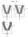
- FIG 10 illustrates modified examples of omnidirectional reflectors disposed on either side of the first waveguide in a mode converter according to the present invention.
- FIG. 10A illustrates the omnidirectional reflector 20 shown in FIG. 1, which is linearly tapered from both sides of the waveguide 10.
- FIGS. 10B and 10C show omnidirectional reflectors 20a and 20b tapered exponentially and in an elliptical or curved shape from both sides of the waveguide 10, respectively.
- the feature of the present invention lies in the use of a forward reflector that is disposed on either side of the low refractive index waveguide 10 and converges a mode onto the high refractive index waveguide 30 for coupling.
- the design details of the mode converter other than described herein conform to the specification of a typical mode converter.
- the present invention achieves a uniform coupling efficiency over a wide wavelength range.
- the mode converter includes omnidirectional reflectors made of the same material as waveguides, thereby simplifying a manufacturing process.
- the mode converter provides a high, bi-directional coupling efficiency regardless of the direction of transmission/reception.
- the mode converter is designed to minimize the optical coupling loss thus allowing the use of a high refractive index waveguide and to simplify the manufacturing process, thereby reducing the size and price of the device.
- the present invention is suitable for use in various devices employing a mode converter such as a coupler for an optical communication transport network.
Landscapes
- Physics & Mathematics (AREA)
- Engineering & Computer Science (AREA)
- Optics & Photonics (AREA)
- General Physics & Mathematics (AREA)
- Chemical & Material Sciences (AREA)
- Microelectronics & Electronic Packaging (AREA)
- Nanotechnology (AREA)
- Life Sciences & Earth Sciences (AREA)
- Biophysics (AREA)
- Crystallography & Structural Chemistry (AREA)
- Power Engineering (AREA)
- Optical Integrated Circuits (AREA)
- Optical Couplings Of Light Guides (AREA)
Applications Claiming Priority (2)
| Application Number | Priority Date | Filing Date | Title |
|---|---|---|---|
| KR1020030092508A KR100543708B1 (ko) | 2003-12-17 | 2003-12-17 | 전 방향성의 반사경을 이용한 광 모드 변환기 |
| KR2003092508 | 2003-12-17 |
Publications (3)
| Publication Number | Publication Date |
|---|---|
| EP1544648A2 true EP1544648A2 (fr) | 2005-06-22 |
| EP1544648A3 EP1544648A3 (fr) | 2005-06-29 |
| EP1544648B1 EP1544648B1 (fr) | 2007-11-07 |
Family
ID=34511240
Family Applications (1)
| Application Number | Title | Priority Date | Filing Date |
|---|---|---|---|
| EP04029915A Expired - Fee Related EP1544648B1 (fr) | 2003-12-17 | 2004-12-16 | Convertisseur de modes utilisant des réflecteurs omnidirectionnels |
Country Status (5)
| Country | Link |
|---|---|
| US (1) | US7236662B2 (fr) |
| EP (1) | EP1544648B1 (fr) |
| JP (1) | JP2005182038A (fr) |
| KR (1) | KR100543708B1 (fr) |
| DE (1) | DE602004009886T2 (fr) |
Families Citing this family (7)
| Publication number | Priority date | Publication date | Assignee | Title |
|---|---|---|---|---|
| US7565046B2 (en) * | 2006-12-13 | 2009-07-21 | Massachusetts Institute Of Technology | Mode transformers for low index high confinement waveguides |
| US9529156B2 (en) * | 2012-06-26 | 2016-12-27 | Acacia Communications, Inc. | Cladding defined transmission grating |
| KR102064908B1 (ko) * | 2013-01-25 | 2020-01-10 | 삼성전자주식회사 | 광 커플링 시스템 및 이를 포함하는 광 센서 |
| US9759864B2 (en) * | 2014-02-28 | 2017-09-12 | Ciena Corporation | Spot-size converter for optical mode conversion and coupling between two waveguides |
| CN105031829B (zh) * | 2015-08-28 | 2018-01-30 | 中国人民解放军第四军医大学 | 一种能量实时反馈式激光理疗仪 |
| KR102143594B1 (ko) * | 2020-02-04 | 2020-08-11 | 국방과학연구소 | 모드 변환 설계자유도가 향상된 광모드 변환기 |
| US11835764B2 (en) * | 2022-01-31 | 2023-12-05 | Globalfoundries U.S. Inc. | Multiple-core heterogeneous waveguide structures including multiple slots |
Citations (5)
| Publication number | Priority date | Publication date | Assignee | Title |
|---|---|---|---|---|
| JP2001051244A (ja) * | 1999-08-11 | 2001-02-23 | Communication Research Laboratory Mpt | フォトニックバンドギャップ構造を用いた光変調器及び光変調方法 |
| US6404952B1 (en) * | 1998-03-26 | 2002-06-11 | Lasercomm Inc. | Optical communication system with chromatic dispersion compensation |
| US20020118916A1 (en) * | 2000-07-10 | 2002-08-29 | Lee Kevin K. | Mode transformer between low index difference waveguide and high index difference waveguide |
| US20020191929A1 (en) * | 1998-10-14 | 2002-12-19 | Massachusetts Institute Of Technology, A Massachusetts Corporation | Omnidirectional multilayer device for enhanced optical waveguiding |
| WO2003023473A1 (fr) * | 2001-09-10 | 2003-03-20 | California Institute Of Technology | Structure et procede de couplage de lumiere entre differents guides d'ondes |
Family Cites Families (1)
| Publication number | Priority date | Publication date | Assignee | Title |
|---|---|---|---|---|
| US7184625B2 (en) * | 2003-02-11 | 2007-02-27 | Luxtera, Inc | Optical waveguide grating coupler incorporating reflective optical elements and anti-reflection elements |
-
2003
- 2003-12-17 KR KR1020030092508A patent/KR100543708B1/ko not_active IP Right Cessation
-
2004
- 2004-12-16 EP EP04029915A patent/EP1544648B1/fr not_active Expired - Fee Related
- 2004-12-16 US US11/012,311 patent/US7236662B2/en not_active Expired - Fee Related
- 2004-12-16 DE DE602004009886T patent/DE602004009886T2/de not_active Expired - Fee Related
- 2004-12-17 JP JP2004366346A patent/JP2005182038A/ja active Pending
Patent Citations (5)
| Publication number | Priority date | Publication date | Assignee | Title |
|---|---|---|---|---|
| US6404952B1 (en) * | 1998-03-26 | 2002-06-11 | Lasercomm Inc. | Optical communication system with chromatic dispersion compensation |
| US20020191929A1 (en) * | 1998-10-14 | 2002-12-19 | Massachusetts Institute Of Technology, A Massachusetts Corporation | Omnidirectional multilayer device for enhanced optical waveguiding |
| JP2001051244A (ja) * | 1999-08-11 | 2001-02-23 | Communication Research Laboratory Mpt | フォトニックバンドギャップ構造を用いた光変調器及び光変調方法 |
| US20020118916A1 (en) * | 2000-07-10 | 2002-08-29 | Lee Kevin K. | Mode transformer between low index difference waveguide and high index difference waveguide |
| WO2003023473A1 (fr) * | 2001-09-10 | 2003-03-20 | California Institute Of Technology | Structure et procede de couplage de lumiere entre differents guides d'ondes |
Non-Patent Citations (4)
| Title |
|---|
| FENNER MILTON A ET AL: "MODE COUPLING IN OPTICAL WAVEGUIDE HORNS" IEEE JOURNAL OF QUANTUM ELECTRONICS, IEEE INC. NEW YORK, US, vol. QE-13, no. 10, October 1977 (1977-10), pages 828-835, XP000563351 ISSN: 0018-9197 * |
| GALARZA M ET AL: "MODE-EXPANDED 1.55-MUM INP-INGAASP FABRY-PEROT LASERS USING ARROW WAVEGUIDES FOR EFFICIENT FIBER COUPLING" IEEE JOURNAL OF SELECTED TOPICS IN QUANTUM ELECTRONICS, IEEE SERVICE CENTER, US, vol. 8, no. 6, November 2002 (2002-11), pages 1389-1398, XP001175370 ISSN: 1077-260X * |
| HADLEY G R: "DESIGN OF TAPERED WAVEGUIDES FOR IMPROVED OUTPUT COUPLING" IEEE PHOTONICS TECHNOLOGY LETTERS, IEEE INC. NEW YORK, US, vol. 5, no. 9, 1 September 1993 (1993-09-01), pages 1068-1070, XP000414180 ISSN: 1041-1135 * |
| PATENT ABSTRACTS OF JAPAN vol. 2000, no. 19, 5 June 2001 (2001-06-05) & JP 2001 051244 A (COMMUNICATION RESEARCH LABORATORY MPT), 23 February 2001 (2001-02-23) * |
Also Published As
| Publication number | Publication date |
|---|---|
| EP1544648A3 (fr) | 2005-06-29 |
| JP2005182038A (ja) | 2005-07-07 |
| EP1544648B1 (fr) | 2007-11-07 |
| KR100543708B1 (ko) | 2006-01-20 |
| US7236662B2 (en) | 2007-06-26 |
| US20050135739A1 (en) | 2005-06-23 |
| DE602004009886D1 (de) | 2007-12-20 |
| DE602004009886T2 (de) | 2008-02-21 |
| KR20050060787A (ko) | 2005-06-22 |
Similar Documents
| Publication | Publication Date | Title |
|---|---|---|
| US7496264B2 (en) | Optical waveguide | |
| JP2004521378A5 (fr) | ||
| US10451797B2 (en) | Few-mode optical fiber | |
| US7480430B2 (en) | Partial confinement photonic crystal waveguides | |
| EP0371675B1 (fr) | Coupleur optique non invasif | |
| CA2352950A1 (fr) | Article comprenant un coupleur a fibres optiques multimode | |
| EP1544648B1 (fr) | Convertisseur de modes utilisant des réflecteurs omnidirectionnels | |
| TW200411239A (en) | Optical coupler apparatus and methods having reduced geometry sensitivity | |
| EP0877284B1 (fr) | Commutateur acousto-optique pour circuit optique en silice | |
| EP0013972A1 (fr) | Corps mélangeur conique pour un élément coupleur de plusieurs fibres optiques | |
| US6748132B1 (en) | Wavelength add drop element for configurable add drop multiplexing | |
| US20230367060A1 (en) | Hollow-core fiber cable and method of manufacturing the same | |
| US7317854B2 (en) | Waveguide and optical coupling device | |
| EP0880048A1 (fr) | Modulateurs acousto-optiques comprenant des guides d'ondes planaires | |
| US6621644B2 (en) | Optical wavelength-demultiplexer with an improved optical lens | |
| CN116520492A (zh) | 一种定向耦合装置 | |
| JP3879521B2 (ja) | 光学素子及び当該光学素子を用いた光トランシーバその他の光学装置 | |
| KR102315387B1 (ko) | 광 통신용 인터페이스 | |
| US11635570B1 (en) | Multi-mode multi-pass delay | |
| CN113985524A (zh) | 一种基于超材料波导的阵列波导光栅 | |
| CN114035269A (zh) | 模斑转换器及其制备方法 | |
| JPS6042715A (ja) | マルチプル−アクセスネツトワ−ク | |
| CN115598764B (zh) | 端面耦合器、光电子芯片和端面耦合器的制作方法 | |
| CN115144962B (zh) | 电磁波传输结构、器件及光芯片 | |
| US11789205B1 (en) | Multi-mode spiral delay device |
Legal Events
| Date | Code | Title | Description |
|---|---|---|---|
| PUAI | Public reference made under article 153(3) epc to a published international application that has entered the european phase |
Free format text: ORIGINAL CODE: 0009012 |
|
| PUAL | Search report despatched |
Free format text: ORIGINAL CODE: 0009013 |
|
| 17P | Request for examination filed |
Effective date: 20041216 |
|
| AK | Designated contracting states |
Kind code of ref document: A2 Designated state(s): AT BE BG CH CY CZ DE DK EE ES FI FR GB GR HU IE IS IT LI LT LU MC NL PL PT RO SE SI SK TR |
|
| AX | Request for extension of the european patent |
Extension state: AL BA HR LV MK YU |
|
| AK | Designated contracting states |
Kind code of ref document: A3 Designated state(s): AT BE BG CH CY CZ DE DK EE ES FI FR GB GR HU IE IS IT LI LT LU MC NL PL PT RO SE SI SK TR |
|
| AX | Request for extension of the european patent |
Extension state: AL BA HR LV MK YU |
|
| AKX | Designation fees paid |
Designated state(s): DE FR GB |
|
| RIN1 | Information on inventor provided before grant (corrected) |
Inventor name: KIM, YOUNG-CHAN Inventor name: HWANG, SEONG-MO,401-1406 CHEONGMYEONG MAEUL Inventor name: KIM, YOUNG-HUN Inventor name: LEE, HONG-SEOK Inventor name: NAM, SEUNG-HO |
|
| 17Q | First examination report despatched |
Effective date: 20051125 |
|
| GRAP | Despatch of communication of intention to grant a patent |
Free format text: ORIGINAL CODE: EPIDOSNIGR1 |
|
| GRAS | Grant fee paid |
Free format text: ORIGINAL CODE: EPIDOSNIGR3 |
|
| GRAA | (expected) grant |
Free format text: ORIGINAL CODE: 0009210 |
|
| AK | Designated contracting states |
Kind code of ref document: B1 Designated state(s): DE FR GB |
|
| REG | Reference to a national code |
Ref country code: GB Ref legal event code: FG4D |
|
| REF | Corresponds to: |
Ref document number: 602004009886 Country of ref document: DE Date of ref document: 20071220 Kind code of ref document: P |
|
| ET | Fr: translation filed | ||
| PLBE | No opposition filed within time limit |
Free format text: ORIGINAL CODE: 0009261 |
|
| STAA | Information on the status of an ep patent application or granted ep patent |
Free format text: STATUS: NO OPPOSITION FILED WITHIN TIME LIMIT |
|
| 26N | No opposition filed |
Effective date: 20080808 |
|
| PGFP | Annual fee paid to national office [announced via postgrant information from national office to epo] |
Ref country code: FR Payment date: 20081212 Year of fee payment: 5 |
|
| PGFP | Annual fee paid to national office [announced via postgrant information from national office to epo] |
Ref country code: DE Payment date: 20081211 Year of fee payment: 5 |
|
| PGFP | Annual fee paid to national office [announced via postgrant information from national office to epo] |
Ref country code: GB Payment date: 20081210 Year of fee payment: 5 |
|
| PG25 | Lapsed in a contracting state [announced via postgrant information from national office to epo] |
Ref country code: FR Free format text: LAPSE BECAUSE OF NON-PAYMENT OF DUE FEES Effective date: 20091231 |
|
| GBPC | Gb: european patent ceased through non-payment of renewal fee |
Effective date: 20091216 |
|
| PG25 | Lapsed in a contracting state [announced via postgrant information from national office to epo] |
Ref country code: DE Free format text: LAPSE BECAUSE OF NON-PAYMENT OF DUE FEES Effective date: 20100701 |
|
| PG25 | Lapsed in a contracting state [announced via postgrant information from national office to epo] |
Ref country code: GB Free format text: LAPSE BECAUSE OF NON-PAYMENT OF DUE FEES Effective date: 20091216 |
|
| REG | Reference to a national code |
Ref country code: FR Ref legal event code: ST Effective date: 20110826 |