EP1542367A2 - Non-linear D/A converter, audio signal processing circuit and liquid crystal display device including the same - Google Patents
Non-linear D/A converter, audio signal processing circuit and liquid crystal display device including the same Download PDFInfo
- Publication number
- EP1542367A2 EP1542367A2 EP04028257A EP04028257A EP1542367A2 EP 1542367 A2 EP1542367 A2 EP 1542367A2 EP 04028257 A EP04028257 A EP 04028257A EP 04028257 A EP04028257 A EP 04028257A EP 1542367 A2 EP1542367 A2 EP 1542367A2
- Authority
- EP
- European Patent Office
- Prior art keywords
- reference voltage
- resistors
- converter
- input digital
- resistor
- Prior art date
- Legal status (The legal status is an assumption and is not a legal conclusion. Google has not performed a legal analysis and makes no representation as to the accuracy of the status listed.)
- Withdrawn
Links
Images





Classifications
-
- G—PHYSICS
- G09—EDUCATION; CRYPTOGRAPHY; DISPLAY; ADVERTISING; SEALS
- G09G—ARRANGEMENTS OR CIRCUITS FOR CONTROL OF INDICATING DEVICES USING STATIC MEANS TO PRESENT VARIABLE INFORMATION
- G09G3/00—Control arrangements or circuits, of interest only in connection with visual indicators other than cathode-ray tubes
- G09G3/20—Control arrangements or circuits, of interest only in connection with visual indicators other than cathode-ray tubes for presentation of an assembly of a number of characters, e.g. a page, by composing the assembly by combination of individual elements arranged in a matrix no fixed position being assigned to or needed to be assigned to the individual characters or partial characters
- G09G3/34—Control arrangements or circuits, of interest only in connection with visual indicators other than cathode-ray tubes for presentation of an assembly of a number of characters, e.g. a page, by composing the assembly by combination of individual elements arranged in a matrix no fixed position being assigned to or needed to be assigned to the individual characters or partial characters by control of light from an independent source
- G09G3/36—Control arrangements or circuits, of interest only in connection with visual indicators other than cathode-ray tubes for presentation of an assembly of a number of characters, e.g. a page, by composing the assembly by combination of individual elements arranged in a matrix no fixed position being assigned to or needed to be assigned to the individual characters or partial characters by control of light from an independent source using liquid crystals
-
- H—ELECTRICITY
- H03—ELECTRONIC CIRCUITRY
- H03M—CODING; DECODING; CODE CONVERSION IN GENERAL
- H03M1/00—Analogue/digital conversion; Digital/analogue conversion
- H03M1/66—Digital/analogue converters
- H03M1/664—Non-linear conversion not otherwise provided for in subgroups of H03M1/66
-
- H—ELECTRICITY
- H03—ELECTRONIC CIRCUITRY
- H03M—CODING; DECODING; CODE CONVERSION IN GENERAL
- H03M1/00—Analogue/digital conversion; Digital/analogue conversion
- H03M1/66—Digital/analogue converters
- H03M1/74—Simultaneous conversion
- H03M1/76—Simultaneous conversion using switching tree
Definitions
- the present invention relates to a D/A converter (digital/analog converter or DAC).
- the invention relates to an audio signal processing circuit having the D/A converter and a liquid crystal display device including the same.
- liquid crystal flat panel displays capable of displaying an image clearly have been widely used and employed as displays for mobile apparatuses such as a mobile phone, a digital camera, a notebook computer, and a PDA (Personal Data Assistant).
- Such a semiconductor device having a display function in many cases, requires an audio circuit for outputting sound in addition to a display portion. Therefore, in conventional display devices, an audio signal processing circuit is generally provided as a dedicated LSI.
- a D/A converter for converting digital data into analog data is essential for such mobile apparatuses.
- a D/A converter as shown in FIG 3 of Patent Document 1, in which an upper limit reference voltage VH and a lower limit reference voltage VL are divided by the capacitance ratio and a divide ratio thereof is changed by changing a combination of capacitors by a switch based on an input digital signal
- a D/A converter as shown in FIG 1 of Patent Document 2 (referred to as a resistor string D/A converter), in which an upper limit reference voltage VH and a lower limit reference voltage VL are divided by a plurality of resistors connected in series therebetween and a divided potential is outputted by selecting one of connections between the resistors based on an input digital signal by a switch.
- an audio signal processing circuit is formed as a dedicated LSI chip
- another printed circuit board is required in addition to a display portion although correct D/A conversion can be realized, which disturbs downsizing and reduction in thickness of a display device.
- non-linear A/D conversion such as a digital signal encoded according to a ⁇ -Law system or an A-Law system
- the input digital signal is required to be performed a data conversion into a digital signal having a linear relationship with an analog signal (linear conversion signal), that is, decoded before D/A conversion.
- a data conversion circuit for converting a non-linear conversion digital signal into a linear conversion digital signal namely a decode circuit (e.g., Look-Up Table) is necessarily provided before a D/A converter. Consequently, space for providing an audio circuit is increased by the decode circuit, making a chip size larger in the case where an audio signal processing circuit is formed as a dedicated LSI chip. It leads to increase of cost and decrease of yield, and makes difficult to form an audio signal processing circuit and a display portion integrally on the same substrate in order to achieve compactness of a display device such as a mobile apparatus.
- a decode circuit e.g., Look-Up Table
- the invention is made in view of solving such problems of a conventional technology.
- the main feature of the invention is to provide a D/A converter to which non-linear conversion digital data such as a digital signal encoded according to a ⁇ -Law system or an A-Law system can be inputted as it is to be converted into an analog signal without a decode circuit, and a semiconductor device including the D/A converter.
- a D/A converter is of a resistor string type, and wherein a resistance value of each of resistors is not set uniform but weighted corresponding to an input signal, namely a digital signal after non-linear A/D conversion.
- a D/A converter comprises a resistor string having a plurality of resistors connected in series between reference voltages and a plurality of switching elements for extracting a potential from respective connections between the plurality of resistors, and wherein the resistors of the resistor string are set at respective resistance values weighted so that a non-linear relationship between an encoded input digital signal and an output analog signal is converted into a linear relationship.
- non-linear conversion digital data can be inputted as it is to be converted into an analog signal
- a decode circuit for converting non-linear conversion digital data into linear conversion digital data is not required. Therefore, more compact device employing a D/A converter can be realized and a configuration of the device can be simplified, leading to higher reliability of the device while decreasing manufacturing cost and improving yield.
- digitalized audio data encoded according to a ⁇ -Law system or an A-Law system can be used as an input digital signal, namely non-linear conversion digital data.
- each of two m-th resistor groups (m is an integral numeral satisfying 1 ⁇ m ⁇ n-1) from both ends connected to the reference voltages includes 2n resistors each having a resistance value of 2 n-m ⁇ R
- each of the middle two n-th resistor groups from the ends connected to the reference voltages includes 2n - 1 resistors each having a resistance value of R
- two connections for extracting a potential are provided between the middle two n-th resistor groups from the ends connected to the reference voltages.
- a decode circuit for converting non-linear conversion digital data into linear conversion digital data is not required. Therefore, more compact analog audio signal processing circuit employing a D/A converter can be realized and a configuration of a device can be simplified, leading to increase the reliability of the device while decreasing manufacturing cost and improving yield.
- the memory circuit can adopt a masked ROM in which digital audio data have been written in advance as a circuit pattern, thereby a step of writing digital audio data into the memory can be omitted. Consequently, a manufacturing step of products of a certain kind can be simplified and cost thereof can be reduced.
- a counter is provided between the control circuit and the memory circuit, thereby data is read out from the memory by increasing or decreasing an address one by one in sequence by the control circuit.
- the audio signal processing circuit may comprise a level shifter between the D/A converter and the control circuit, and between the memory circuit and the D/A converter, thereby a logic level is converted in transmitting a control signal so that the D/Aconverter can be driven with high voltage.
- a liquid crystal display device including the D/A converter according to the invention comprises a substrate, a pixel portion having thin film transistors formed on the substrate, a driver circuit portion having thin film transistors formed on the substrate and for driving the pixel portion, an opposing substrate provided opposite to the substrate, a sealing member provided between the substrate and the opposing substrate, and liquid crystal filled in the region surrounded by the substrate, the opposing substrate and the sealing member.
- An audio signal processing circuit for supplying an analog audio signal formed on the substrate is further provided.
- the audio signal processing circuit comprises a memory circuit for storing digital audio data, a D/A converter for receiving an encoded digital signal from the memory circuit and then converting into an analog signal, an analog circuit for amplifying and outputting the analog signal received from the D/A converter, and a control circuit for controlling the memory circuit and the D/A converter, wherein the D/A converter comprises a resistor string having a plurality of resistors connected in series between reference voltages and a plurality of switching elements for extracting a potential from respective connections between the plurality of resistors, and the resistors of the resistor string are set at respective resistance values weighted so that a non-linear relationship between an encoded input digital signal and an output analog signal is converted into a linear relationship.
- a decode circuit for converting non-linear conversion digital data into linear conversion digital data is not required. Therefore, more compact liquid crystal display device including a D/A converter can be realized and a configuration of a device can be simplified, leading to increase the reliability of the device while decreasing manufacturing cost and improving yield.
- liquid crystal display device described above may comprise a speaker provided on the substrate and connected to the audio signal processing circuit. Accordingly, a compact unit can be configured in which a speaker and a liquid crystal display portion are provided integrally on the same substrate and can be applied to various mobile apparatuses, leading to achieve further lightweight, thinness, and compactness of a device.
- a D/A converter can be inputted with non-linear conversion digital data such as a digital signal encoded according to a ⁇ -Law system or an A-Law system as it is to be converted into an analog signal, thereby a decode circuit for converting a non-linear conversion digital signal into a linear conversion digital signal is not required. Consequently, reduction of space and simplification of configuration of an audio signal processing circuit including a D/A converter can be achieved, which realizes a compact semiconductor device including a D/A converter at a low manufacturing cost.
- FIG. 1 is a conceptual diagram of a general resistor string D/A converter.
- the resistor string D/A converter in the case of input digital data of n-bit (n is an integral numeral of two or more), 2 n or 2 n - 1 resistors (unit resistors) are connected in series between an upper limit reference voltage VH and a lower limit reference voltage VL to form a resistor line in a string form (a resistor string).
- One of connections between the resistors is selected by switch groups for output selection to output a divided potential by the resistors.
- resistors 101 to 107 connected between VH and VL constitute a resistor string, one of eight connections between the resistors is selected by controlling each of a first switch group of switches for output selection 108 to 115, a second switch group of switches for output selection 116 to 119, and a third switch group of switches for output selection 120 and 121 based on 3-bit digital data, so that an analog signal divided by the resistors is outputted through a buffer amplifier 123 and an output terminal 122.
- resistance of each of resistors is not set uniform but weighted, thereby a potential is weighted to be divided. Accordingly, in the case where an input digital signal is a digital signal converted non-linearly from an analog signal (non-linear conversion signal) such as a digital signal encoded according to a ⁇ -Law system or an A-Law system, a non-linear relationship between the input digital signal and an output analog signal can be converted into a linear relationship while converting the encoded input digital signal into the analog signal. Therefore, the non-linear conversion digital signal can be directly inputted to a D/A converter without a decode circuit for converting a non-linear conversion digital signal into a linear conversion digital signal.
- an analog signal non-linear conversion signal
- ⁇ -Law system and A-Law system are audio data compression technologies for a mobile phone and the like, and the ⁇ -Law system is employed in Japan and US whereas the A-Law system is employed in Europe in practice.
- Table 1 an analog input (amplitude) and a digital output do not form a proportionate relationship and a whole analog signal is divided into 16 segments (8 segments in both positive and negative directions, respectively) corresponding to more significant 4 bits of a digital output.
- each of the segments is further divided into 16 steps uniformly corresponding to less significant 4 bits of the digital output to quantize an analog input.
- FIG 2 shows a concept of a logarithmic compressive conversion of a ⁇ -Law system.
- a corresponding digital value is taken in smaller steps in a small amplitude of an input signal compared to in a large amplitude of the input signal. Therefore, a Look-Up Table which is a decode circuit for converting non-linear conversion digital data (input digital data) encoded according to the ⁇ -Law system into linear conversion digital data (output digital data) that is used in a conventional technology has a property shown in FIG 3.
- the D/A converter according to the invention is provided with the digital data conversion function as shown in FIG. 3 by weighting respective resistance values of resistors in the resistor string D/A converter, thus the decode circuit such as the Look-Up Table is not required.
- FIG 4 shows an example of a resister string of a resistor string D/A converter in which respective resistance values of resistors are weighted according to the invention as described above.
- the resister string shown in FIG 4 is a configuration example in the case of an 8-bit input signal in ⁇ -Law format, which is weighted so that a non-linear relationship between the 8-bit input digital signal encoded according to the ⁇ -Law system and an output analog signal is converted into a linear relationship.
- a resistor string of a D/A converter has 2n groups of resistors and wherein each of the two m-th resistor groups (m is an integral numeral satisfying 1 ⁇ m ⁇ n-1) from ends connected to the reference voltages includes 2n resistors each having a resistance value of 2 n-m .
- each of the middle two n-th resistor groups from the ends connected to the reference voltages includes 2n - 1 resistors each having a resistance value of R, and two connections for extracting a potential are provided between the middle two n-th resistor groups from the ends.
- a configuration of a resistor string as mentioned above, namely a pattern of weighting respective resistors depends on the number of bits of an input digital signal, namely a non-linear characteristic of a relationship between an encoded input digital signal and an output analog signal. For instance, in the case of an input digital signal in A-Law format, another pattern of weighting respective resistors is set.
- an audio signal processing circuit as illustrated in FIG. 5 can be configured.
- either digital data stored in a memory circuit 501 or digital data supplied externally through an external interface circuit 503 is selected by a selection circuit 504 under the control of a control circuit 502, then inputted to a resistor string D/A converter 505 of the invention directly as an input digital signal.
- the input digital signal is converted into an analog signal in the resistor string D/A converter 505 to be supplied to an analog circuit 506.
- the resistor string D/A converter 505 comprises a resistor string having a plurality of resistors, in which respective resistance values are set such that a non-linear relationship between an encoded input digital signal and an output analog signal is converted into a linear relationship. Accordingly, in view of adopting for an audio circuit of a digital apparatuse and the like, a decode circuit for converting non-linear conversion digital data into linear conversion digital data such as a Look-Up Table with a property as shown in FIG. 3 is not required to be provided before a D/A converter, unlike a conventional audio signal processing circuit. Therefore, as compared to the conventional audio signal processing circuit, an audio signal processing circuit can be configured in a small space, contributing to downsizing of a device. In addition, a circuit configuration can be simplified, leading to lower manufacturing cost and higher yield while higher reliability of a device.
- a memory circuit of an audio signal processing circuit as described above can adopt a memory such as an SRAM, a DRAM, and a flash memory, though the invention is not limited to these.
- a masked ROM that has a configuration including an X decoder 601 and a Y decoder 602 as shown in FIG. 6 and has a circuit pattern of digital audio data which has been written in advance may be adopted.
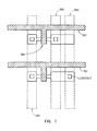
- FIG. 7 shows an example of a masked ROM, in which one memory cell comprises a word line 701, a bit line 702, a high potential line 703, a low potential line 704, and a memory transistor 705.
- the memory transistor 705 one of a source and a drain is connected to the bit line 702 whereas the other is connected to the high potential line 703 or the low potential line 704.
- the memory cell is determined whether to become Hi (high potential state) or Low (low potential state) depending on whether on a low potential line side or on a high potential line side a connection between silicon forming the source and the drain and a wiring is provided in the transistor.
- the memory transistor 705 is an N-channel transistor
- the word line 701 becomes Hi
- the bit line 702 is shorted to one of the high potential line 703 and the low potential line 704 through the memory transistor 705 and Hi or Low potential is generated in the bit line 702.
- This potential is amplified by a sense amplifier and outputted, thereby data can be obtained.
- a step of writing digital audio data into a memory is omitted. Consequently, a manufacturing step of products of certain kind can be simplified and cost thereof can be reduced.
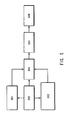
- FIG. 8 illustrates one example of a control circuit used in the above-described audio signal processing circuit. It can be controlled externally, though can be controlled internally as well by a signal of a CPU 801 which is integrally formed with an audio signal processing circuit as shown in FIG. 8.
- a counter 803 may be provided between a control circuit 802 and the memory circuit 804 as shown in FIG. 8, thereby data is read out from the memory circuit 804 by counting addresses in descending order or in ascending order in sequence.
- level shifters 805 for converting a logic level in transmitting a control signal are provided between the control circuit 802 and a D/A converter 806, and between the memory circuit 804 and the D/A converter 806, thereby the D/A converter 806 can be driven with high voltage (e.g., the same voltage as that of a signal line driver circuit).
- a converted analog signal is supplied to an analog circuit 807.
- FIGS. 9A and 9B are a top plan view and a side view respectively, showing an example of a liquid crystal display device including a D/A converter according to the invention.
- TFTs thin film transistors
- a source signal line driver circuit 902 a gate signal line driver circuit 903, a pixel portion 904, a memory circuit 911, a control circuit 912, a D/A converter 913, and an analog circuit 914 are integrally formed.
- the source signal line driver circuit 902, the gate signal line driver circuit 903, and the pixel portion 904 constitute a display portion.
- Signals required for the gate signal line driver circuit 903 are inputted externally from an FPC (flexible printed circuit board) 907.
- Liquid crystal is filled in the region surrounded by the substrate 909, a sealing member, and an opposing substrate 910 which is provided so as to sandwich the sealing member on the substrate 909.
- the memory circuit 911, the control circuit 912, the D/A converter 913, and the analog circuit 914 constitute an audio signal processing circuit 905.
- a speaker 906 mounted on the substrate 909 is connected to the audio signal processing circuit 905 by an FPC 908.
- Digital audio data is stored in the memory circuit 911 of the audio signal processing circuit 905 and converted into an analog signal in the D/A converter 913, and then the analog signal is outputted as a sound though the analog circuit 914 and the speaker 906.
- resistors of a resistor string can be made of an impurity diffusion layer or a polysilicon film in a semiconductor thin film, and switches for output selection can be made of thin film transistors.
- a decode circuit for converting a non-linear conversion digital signal into a linear conversion digital signal is not required in the audio signal processing circuit 905, enabling reduction in area of the audio signal processing circuit 905.
- This space reduction of the audio signal processing circuit 905 realizes a compact unit for providing sound and image at the same time, in which a display portion and an audio output portion are integrally formed on one substrate, such as the liquid crystal display device shown in FIG 9.
- the thickness of the opposing substrate 910 and the substrate 909 are in general approximately 0.7 mm respectively in this unit. Therefore, by adopting a speaker of thin type, the maximum thickness of the unit (normally, a speaker portion is the thickest) can result in 2 mm or less.
- the thickness of a speaker that is provided outside of a substrate is in general approximately 7 mm, therefore, a thin type speaker is provided on the same substrate so that volume occupied by a speaker within a device can be reduced.
- a decode circuit is not required in the audio signal processing circuit 905, a space thereof can be applied to a larger memory circuit so that a larger amount of data can be stored therein.
- a liquid crystal material is mainly used for a display portion in a semiconductor device of this type, however, the invention is not exclusively limited to this and any configuration that is known to those skilled in the art can be adopted as long as it has a similar display function.
- a D/A converter according to the invention can be inputted with non-linear conversion digital data such as a digital signal encoded according to a ⁇ -Law system or an A-Law system as it is to convert into an analog signal. Consequently, a decode circuit for converting a non-linear conversion digital signal into a linear conversion digital signal is not required and a device can be more compact. Therefore, the D/A converter according to the invention is useful for any semiconductor device including a D/A converter.
Landscapes
- Engineering & Computer Science (AREA)
- Physics & Mathematics (AREA)
- Theoretical Computer Science (AREA)
- Nonlinear Science (AREA)
- Chemical & Material Sciences (AREA)
- Crystallography & Structural Chemistry (AREA)
- Computer Hardware Design (AREA)
- General Physics & Mathematics (AREA)
- Analogue/Digital Conversion (AREA)
Abstract
Description
| Sign Bit | Segment Bit | Step Bit | Sign | Step Side × Number of Steps | Analog Input (Amplitude) | |||
| 1 | 0 | 0 | 0 | 0000 | 2031+128 × 16 | 4079 | ||
| 1111 | 2031+128 | 2159 | ||||||
| 1 | 0 | 0 | 1 | 0000 | 1007+64 × 16 | 2031 | ||
| 1111 | 1007+64 | 1071 | ||||||
| 1 | 0 | 1 | 0 | 0000 | 495+32 × 16 | 1007 | ||
| 1111 | 495+32 | 527 | ||||||
| 1 | 0 | 1 | 1 | 0000 | 239+16 × 16 | 495 | ||
| 1111 | 239+16 | 255 | ||||||
| 1 | 1 | 0 | 0 | 0000 | 118+8 × 16 | 239 | ||
| 1111 | 111+8 | 119 | ||||||
| 1 | 1 | 0 | 1 | 0000 | 47+4 × 16 | 111 | ||
| 1111 | 47+4 | 52 | ||||||
| 1 | 1 | 1 | 0 | 0000 | 15+2 × 16 | 47 | ||
| 1111 | 15+2 | 17 | ||||||
| 1 | 1 | 1 | 1 | 0000 | 15 | 15 | ||
| 1110 | 1 | 1 | ||||||
| 1111 | 0 | 0 | ||||||
| 0 | 1 | 1 | 1 | 1111 | - | 0 | 0 | |
| 1110 | - | 1 | 1 | |||||
| 0000 | - | 15 | 15 | |||||
| 0 | 1 | 1 | 0 | 1111 | - | 15+2 | 17 | |
| 0000 | - | 15+2 × 16 | 98 | |||||
| 0 | 1 | 0 | 1 | 1111 | - | 47+4 | 104 | |
| 0000 | - | 47+4 × 16 | 111 | |||||
| 0 | 1 | 0 | 0 | 1111 | - | 111+8 | 119 | |
| 0000 | - | 111 +8 × 16 | 239 | |||||
| 0 | 0 | 1 | 1 | 1111 | - | 239+16 | 255 | |
| 0000 | - | 239+16 × 16 | 495 | |||||
| 0 | 0 | 1 | 0 | 1111 | - | 495+32 | 527 | |
| 0000 | - | 495+32 × 16 | 1007 | |||||
| 0 | 0 | 0 | 1 | 1111 | - | 1007+64 | 1071 | |
| 0000 | - | 1007+64 × 16 | 2031 | |||||
| 0 | 0 | 0 | 0 | 1111 | - | 2031+128 | 2159 | |
| 0000 | - | 2031+128 × 16 | 4079 |
Claims (16)
- A D/A converter comprising:wherein the plurality of switching elements are controlled by an input digital data,a first reference voltage;a second reference voltage;a plurality of resistors connected in series between the first reference voltage and the second reference voltage; anda plurality of switching elements;
wherein the plurality of switching elements extract a potential from selected one of connecting portions between the plurality of resistors,
wherein the input digital data is a non-linear conversion digital signal, and
wherein resistance values of the plurality of the resistors are set so that the potential is a linear conversion analog signal. - A D/A converter according to claim 1, wherein the input digital data is digitalized data encoded according to a µ-Law system.
- A D/A converter according to claim 1, wherein the input digital data is digitalized data encoded according to an A-Law system.
- A D/A converter according to claim 2,
wherein the input digital signal is a digitalized n-bit signal, n is an integral numeral of two or more, encoded according to a µ-Law system,
wherein the plurality of resistor is 2n resistor groups,
wherein a m-th resistor group, m is an integral numeral satisfying 1 ≤ m ≤ (n-1), from the first reference voltage includes 2n resistors each having a resistance value of 2n-m. R,
wherein a m-th resistor group from the second reference voltage includes 2n resistors each having a resistance value of (2n-m · R),
wherein a n-th resistor groups from the first reference voltage includes (2n - 1) resistors each having a resistance value of R,
wherein a n-th resistor groups from the second reference voltage includes (2n - 1) resistors each having a resistance value of R, and
wherein two connections for extracting the potential are provided between the n-th resistor groups from the first reference voltage and the n-th resistor groups from the second reference voltage. - An audio signal processing circuit comprising:wherein the plurality of switching elements are controlled by an input digital audio data,a memory circuit storing an input digital audio data;a D/A converter comprising:a first reference voltage;a second reference voltage;a plurality of resistors connected in series between the first reference voltage and the second reference voltage; anda plurality of switching elements;an analog circuit connected to the D/A converter; anda control circuit connected to a memory circuit and the D/A converter;
wherein the plurality of switching elements extract a potential from selected one of connecting portions between the plurality of resistors,
wherein the input digital audio data is a non-linear conversion digital signal, and
wherein resistance values of the plurality of the resistors are set so that the potential is a linear conversion analog audio signal. - An audio signal processing circuit according to claim 5, wherein the input digital audio data is digitalized data encoded according to a µ-Law system.
- An audio signal processing circuit according to claim 5, wherein the input digital audio data is digitalized data encoded according to an A-Law system.
- An audio signal processing circuit according to claim 6,
wherein the input digital audio signal is a digitalized n-bit signal, n is an integral numeral of two or more, encoded according to a µ-Law system,
wherein the plurality of resistor is 2n resistor groups,
wherein a m-th resistor group, m is an integral numeral satisfying 1 ≤ m ≤ (n-1), from the first reference voltage includes 2n resistors each having a resistance value of 2n-m. R,
wherein a m-th resistor group from the second reference voltage includes 2n resistors each having a resistance value of (2n-m. R),
wherein a n-th resistor groups from the first reference voltage includes (2n - 1) resistors each having a resistance value of R,
wherein a n-th resistor groups from the second reference voltage includes (2n - 1) resistors each having a resistance value of R, and
wherein two connections for extracting the potential are provided between the n-th resistor groups from the first reference voltage and the n-th resistor groups from the second reference voltage. - An audio signal processing circuit according to claim 5, wherein the memory circuit is a masked ROM in which digital audio data has been written in advance as a circuit pattern
- An audio signal processing circuit according to claim 5, wherein a counter is provided between the control circuit and the memory circuit, thereby data is read out from a memory by increasing or decreasing an address one by one in sequence by the control circuit.
- An audio signal processing circuit according to claim 5, wherein a level shifter is provided between the D/A converter and the control circuit, and between the memory circuit and the D/A converter.
- A liquid crystal display device comprising:wherein the plurality of switching elements are controlled by an input digital audio data,a substrate;a pixel portion having a first thin film transistor formed over the substrate;a driver circuit portion having a second thin film transistor formed over the substrate, connected to the pixel portion;an opposing substrate provided opposite to the substrate;a sealing member provided between the substrate and the opposing substrate;liquid crystal provided in a region surrounded by the substrate, the opposing substrate and the sealing member, andan audio signal processing circuit formed over the substrate comprising:a memory circuit storing an input digital audio data;a D/A converter comprising:a first reference voltage;a second reference voltage;a plurality of resistors connected in series between the first reference voltage and the second reference voltage; anda plurality of switching elements;an analog circuit connected to the D/A converter; anda control circuit connected to a memory circuit and the D/A converter;
wherein the plurality of switching elements extract a potential from selected one of connecting portions between the plurality of resistors,
wherein the input digital audio data is a non-linear conversion digital signal, and
wherein resistance values of the plurality of the resistors are set so that the potential is a linear conversion analog audio signal. - A liquid crystal display device according to claim 12, wherein the input digital audio data is digitalized data encoded according to a µ-Law system.
- A liquid crystal display device according to claim 12, wherein the input digital audio data is digitalized data encoded according to an A-Law system.
- A liquid crystal display device according to claim 13,
wherein the input digital audio signal is a digitalized n-bit signal, n is an integral numeral of two or more, encoded according to a µ-Law system,
wherein the plurality of resistor is 2n resistor groups,
wherein a m-th resistor group, m is an integral numeral satisfying 1 ≤ m ≤ (n-1), from the first reference voltage includes 2n resistors each having a resistance value of 2n-m· R,
wherein a m-th resistor group from the second reference voltage includes 2n resistors each having a resistance value of (2n-m · R),
wherein a n-th resistor groups from the first reference voltage includes (2n - 1) resistors each having a resistance value of R,
wherein a n-th resistor groups from the second reference voltage includes (2n - 1) resistors each having a resistance value of R, and
wherein two connections for extracting the potential are provided between the n-th resistor groups from the first reference voltage and the n-th resistor groups from the second reference voltage. - A liquid crystal display device according to claim 12, wherein a speaker is mounted on the substrate and connected. to the audio signal processing circuit.
Applications Claiming Priority (2)
| Application Number | Priority Date | Filing Date | Title |
|---|---|---|---|
| JP2003413156 | 2003-12-11 | ||
| JP2003413156A JP4629971B2 (en) | 2003-12-11 | 2003-12-11 | Nonlinear A / D converted digital signal compatible D / A conversion circuit, audio signal processing circuit incorporating the same, and display device |
Publications (2)
| Publication Number | Publication Date |
|---|---|
| EP1542367A2 true EP1542367A2 (en) | 2005-06-15 |
| EP1542367A3 EP1542367A3 (en) | 2006-05-10 |
Family
ID=34510540
Family Applications (1)
| Application Number | Title | Priority Date | Filing Date |
|---|---|---|---|
| EP04028257A Withdrawn EP1542367A3 (en) | 2003-12-11 | 2004-11-29 | Non-linear D/A converter, audio signal processing circuit and liquid crystal display device including the same |
Country Status (6)
| Country | Link |
|---|---|
| US (1) | US7369074B2 (en) |
| EP (1) | EP1542367A3 (en) |
| JP (1) | JP4629971B2 (en) |
| KR (1) | KR101111989B1 (en) |
| CN (1) | CN100530975C (en) |
| TW (1) | TWI350064B (en) |
Cited By (2)
| Publication number | Priority date | Publication date | Assignee | Title |
|---|---|---|---|---|
| WO2012078922A3 (en) * | 2010-12-09 | 2012-08-09 | Qualcomm Incorporated | A digital-to-analog converter with non-uniform resolution |
| GB2590513A (en) * | 2019-12-17 | 2021-06-30 | Cirrus Logic Int Semiconductor Ltd | Digital to analog converters |
Families Citing this family (16)
| Publication number | Priority date | Publication date | Assignee | Title |
|---|---|---|---|---|
| US8280345B2 (en) | 2000-12-22 | 2012-10-02 | Google Inc. | LPRF device wake up using wireless tag |
| US20080303897A1 (en) | 2000-12-22 | 2008-12-11 | Terahop Networks, Inc. | Visually capturing and monitoring contents and events of cargo container |
| US7522568B2 (en) * | 2000-12-22 | 2009-04-21 | Terahop Networks, Inc. | Propagating ad hoc wireless networks based on common designation and routine |
| US8315563B2 (en) * | 2000-12-22 | 2012-11-20 | Google Inc. | Wireless reader tags (WRTs) with sensor components in asset monitoring and tracking systems |
| ATE490602T1 (en) * | 2004-07-06 | 2010-12-15 | Kenet Inc | VOLTAGE RANDOM ACCESS MEMORY (VRAM) |
| JP4639153B2 (en) * | 2006-01-20 | 2011-02-23 | Okiセミコンダクタ株式会社 | Digital / analog converter |
| JP2008160782A (en) * | 2006-01-31 | 2008-07-10 | Matsushita Electric Ind Co Ltd | Digital / analog converter |
| JP2008022301A (en) * | 2006-07-13 | 2008-01-31 | Sony Corp | D / A converter |
| JP5116269B2 (en) * | 2006-08-25 | 2013-01-09 | 株式会社ジャパンディスプレイイースト | Image display device |
| JP4627773B2 (en) * | 2007-10-16 | 2011-02-09 | Okiセミコンダクタ株式会社 | Drive circuit device |
| KR20100041151A (en) * | 2008-10-13 | 2010-04-22 | 삼성전자주식회사 | Switch circuit, dc-dc converter and display driver ic including the same |
| US8705523B2 (en) | 2009-02-05 | 2014-04-22 | Google Inc. | Conjoined class-based networking |
| US9112790B2 (en) | 2013-06-25 | 2015-08-18 | Google Inc. | Fabric network |
| CN103745695B (en) * | 2013-12-02 | 2016-03-30 | 深圳市华星光电技术有限公司 | Gamma Voltag driving circuit, source drive module and liquid crystal panel |
| JP6504345B2 (en) | 2015-02-04 | 2019-04-24 | セイコーエプソン株式会社 | D / A converter circuit, oscillator, electronic device and moving body |
| US10096631B2 (en) | 2015-11-30 | 2018-10-09 | Semiconductor Energy Laboratory Co., Ltd. | Signal processing circuit and semiconductor device including the signal processing circuit |
Family Cites Families (28)
| Publication number | Priority date | Publication date | Assignee | Title |
|---|---|---|---|---|
| US3997892A (en) * | 1973-07-27 | 1976-12-14 | Trw Inc. | Digital to analog converter with improved companding |
| SE386790B (en) * | 1975-09-26 | 1976-08-16 | Ellemtel Utvecklings Ab | DIGITAL ANALOG CONVERTER |
| NL7511840A (en) * | 1975-10-09 | 1977-04-13 | Philips Nv | DIGITAL ANALOG CONVERTER. |
| US4126853A (en) * | 1975-11-05 | 1978-11-21 | Rockwell International Corporation | Non-linear digital-to analog conversion |
| US4160244A (en) | 1976-02-25 | 1979-07-03 | National Semiconductor Corporation | Conversion circuit |
| US4146882A (en) * | 1976-08-24 | 1979-03-27 | Intel Corporation | Digital-to-analog converter employing two levels of decoding |
| DE2836079C2 (en) * | 1978-08-17 | 1986-01-16 | Siemens AG, 1000 Berlin und 8000 München | Digital-to-analog converter |
| US4385286A (en) * | 1980-07-18 | 1983-05-24 | American Microsystems, Inc. | Use of single reference voltage for analog to digital or digital to analog conversion of bipolar signals |
| US4594576A (en) * | 1983-06-24 | 1986-06-10 | Matsushita Electric Industrial Company, Limited | Circuit arrangement for A/D and/or D/A conversion with nonlinear D/A conversion |
| US4933675A (en) * | 1987-03-19 | 1990-06-12 | Beard Terry D | Audio digital/analog encoding and decoding |
| US4983973A (en) * | 1989-05-22 | 1991-01-08 | Brooktree Corporation | Non-linear analog-to-digital converter |
| US5643804A (en) | 1993-05-21 | 1997-07-01 | Semiconductor Energy Laboratory Co., Ltd. | Method of manufacturing a hybrid integrated circuit component having a laminated body |
| JPH0822024A (en) | 1994-07-05 | 1996-01-23 | Mitsubishi Electric Corp | Active matrix substrate and manufacturing method thereof |
| US5841384A (en) * | 1994-08-18 | 1998-11-24 | Hughes Electronics | Non-linear digital-to-analog converter and related high precision current sources |
| JP2762969B2 (en) | 1995-09-06 | 1998-06-11 | 日本電気株式会社 | Resistor string type D / A converter and serial / parallel type A / D converter |
| US5991278A (en) * | 1996-08-13 | 1999-11-23 | Telogy Networks, Inc. | Asymmetric modem communications system and method |
| US5729226A (en) * | 1996-08-23 | 1998-03-17 | Paradyne Corporation | Rob bit compensation system and method associated with a transmitter or CODEC |
| JP3403027B2 (en) * | 1996-10-18 | 2003-05-06 | キヤノン株式会社 | Video horizontal circuit |
| US6233554B1 (en) * | 1997-12-12 | 2001-05-15 | Qualcomm Incorporated | Audio CODEC with AGC controlled by a VOCODER |
| GB2333408A (en) * | 1998-01-17 | 1999-07-21 | Sharp Kk | Non-linear digital-to-analog converter |
| KR100282447B1 (en) * | 1998-08-18 | 2001-02-15 | 김영환 | Nonlinear Digital / Analog Converter |
| US6295013B1 (en) * | 1998-09-25 | 2001-09-25 | Photobit Corporation | Nonlinear flash analog to digital converter used in an active pixel system |
| US6420988B1 (en) | 1998-12-03 | 2002-07-16 | Semiconductor Energy Laboratory Co., Ltd. | Digital analog converter and electronic device using the same |
| US6239731B1 (en) * | 1999-05-11 | 2001-05-29 | Texas Instruments Incorporated | Data converter with reduced supply and resistor string voltages |
| TW521223B (en) | 1999-05-17 | 2003-02-21 | Semiconductor Energy Lab | D/A conversion circuit and semiconductor device |
| GB2366440A (en) * | 2000-09-05 | 2002-03-06 | Sharp Kk | Driving arrangement for active matrix LCDs |
| US6445325B1 (en) | 2001-08-30 | 2002-09-03 | Texas Instruments Incorporated | Piecewise linear digital to analog conversion |
| KR100477158B1 (en) * | 2001-12-18 | 2005-03-17 | 매그나칩 반도체 유한회사 | Cmos image sensor with digital-analog converter |
-
2003
- 2003-12-11 JP JP2003413156A patent/JP4629971B2/en not_active Expired - Fee Related
-
2004
- 2004-11-24 TW TW093136173A patent/TWI350064B/en not_active IP Right Cessation
- 2004-11-29 EP EP04028257A patent/EP1542367A3/en not_active Withdrawn
- 2004-11-29 US US10/997,918 patent/US7369074B2/en not_active Expired - Fee Related
- 2004-12-10 CN CNB2004101002655A patent/CN100530975C/en not_active Expired - Fee Related
- 2004-12-10 KR KR1020040104014A patent/KR101111989B1/en not_active Expired - Fee Related
Cited By (8)
| Publication number | Priority date | Publication date | Assignee | Title |
|---|---|---|---|---|
| WO2012078922A3 (en) * | 2010-12-09 | 2012-08-09 | Qualcomm Incorporated | A digital-to-analog converter with non-uniform resolution |
| US8462036B2 (en) | 2010-12-09 | 2013-06-11 | Qualcomm, Incorporated | Digital-to-analog converter with non-uniform resolution |
| US9059733B2 (en) | 2010-12-09 | 2015-06-16 | Qualcomm Incorporated | Digital-to-analog converter with non-uniform resolution |
| GB2590513A (en) * | 2019-12-17 | 2021-06-30 | Cirrus Logic Int Semiconductor Ltd | Digital to analog converters |
| GB2590513B (en) * | 2019-12-17 | 2021-11-24 | Cirrus Logic Int Semiconductor Ltd | Non-monotonic digital to analog converters |
| US11303294B2 (en) | 2019-12-17 | 2022-04-12 | Cirrus Logic, Inc. | Digital to analog converters |
| US11949427B2 (en) | 2019-12-17 | 2024-04-02 | Cirrus Logic Inc. | Force sensing systems |
| US12166502B2 (en) | 2019-12-17 | 2024-12-10 | Cirrus Logic Inc. | Force sensing systems |
Also Published As
| Publication number | Publication date |
|---|---|
| TWI350064B (en) | 2011-10-01 |
| CN100530975C (en) | 2009-08-19 |
| US7369074B2 (en) | 2008-05-06 |
| TW200520395A (en) | 2005-06-16 |
| KR101111989B1 (en) | 2012-03-13 |
| JP2005175898A (en) | 2005-06-30 |
| CN1627645A (en) | 2005-06-15 |
| KR20050058214A (en) | 2005-06-16 |
| US20050128112A1 (en) | 2005-06-16 |
| EP1542367A3 (en) | 2006-05-10 |
| JP4629971B2 (en) | 2011-02-09 |
Similar Documents
| Publication | Publication Date | Title |
|---|---|---|
| US7369074B2 (en) | D/A converter for a digital signal after non-linear A/D conversion, audio signal processing circuit and liquid crystal display device including the same | |
| US8379000B2 (en) | Digital-to-analog converting circuit, data driver and display device | |
| US7978168B2 (en) | D/A converter | |
| CN101419769B (en) | Digital simulation conversion circuit, data driver and display unit | |
| US20090273388A1 (en) | Miniaturized demultiplexer and electronic device using same | |
| TWI354285B (en) | Memory curcuit | |
| EP2061025A2 (en) | Sub-pixel devices for active matrix display | |
| US20090096818A1 (en) | Data driver, integrated circuit device, and electronic instrument | |
| CN100511405C (en) | Integrated circuit device and electronic instrument | |
| US7245283B2 (en) | LCD source driving circuit having reduced structure including multiplexing-latch circuits | |
| US20090160849A1 (en) | Integrated circuit device, electro-optical device, and electronic instrument | |
| CN101178871A (en) | Data driver and organic light emitting diode display device thereof | |
| US8174475B2 (en) | D/A conversion circuit, data driver, integrated circuit device, and electronic instrument | |
| US8179389B2 (en) | Compact layout structure for decoder with pre-decoding and source driving circuit using the same | |
| US10735011B2 (en) | Digital-to-analog converter and driving circuit of display device having the same | |
| KR20080002683A (en) | D / A converter circuit, liquid crystal drive circuit, and liquid crystal display device | |
| CN101739924B (en) | Driver device | |
| US20050024317A1 (en) | Display device | |
| CN101441843A (en) | Image display system | |
| US20090160881A1 (en) | Integrated circuit device, electro-optical device, and electronic instrument | |
| US7006176B2 (en) | Liquid crystal display device comprising a C-DAC and wherein a light blocking film opposes the C-DAC and contacts the liquid crystal | |
| JPH11274932A (en) | Digital-to-analog converter circuit and semiconductor device | |
| US7411536B1 (en) | Digital-to-analog converter | |
| KR100965593B1 (en) | Driving device of liquid crystal display | |
| US20250148989A1 (en) | Display device and an electronic device including the same |
Legal Events
| Date | Code | Title | Description |
|---|---|---|---|
| PUAI | Public reference made under article 153(3) epc to a published international application that has entered the european phase |
Free format text: ORIGINAL CODE: 0009012 |
|
| AK | Designated contracting states |
Kind code of ref document: A2 Designated state(s): AT BE BG CH CY CZ DE DK EE ES FI FR GB GR HU IE IS IT LI LU MC NL PL PT RO SE SI SK TR |
|
| AX | Request for extension of the european patent |
Extension state: AL HR LT LV MK YU |
|
| PUAL | Search report despatched |
Free format text: ORIGINAL CODE: 0009013 |
|
| AK | Designated contracting states |
Kind code of ref document: A3 Designated state(s): AT BE BG CH CY CZ DE DK EE ES FI FR GB GR HU IE IS IT LI LU MC NL PL PT RO SE SI SK TR |
|
| AX | Request for extension of the european patent |
Extension state: AL HR LT LV MK YU |
|
| 17P | Request for examination filed |
Effective date: 20060919 |
|
| 17Q | First examination report despatched |
Effective date: 20061122 |
|
| AKX | Designation fees paid |
Designated state(s): DE FI FR GB NL |
|
| STAA | Information on the status of an ep patent application or granted ep patent |
Free format text: STATUS: THE APPLICATION IS DEEMED TO BE WITHDRAWN |
|
| 18D | Application deemed to be withdrawn |
Effective date: 20140603 |