EP1542358A1 - AGC system, AGC method, and receiver using the AGC system - Google Patents
AGC system, AGC method, and receiver using the AGC system Download PDFInfo
- Publication number
- EP1542358A1 EP1542358A1 EP20040029197 EP04029197A EP1542358A1 EP 1542358 A1 EP1542358 A1 EP 1542358A1 EP 20040029197 EP20040029197 EP 20040029197 EP 04029197 A EP04029197 A EP 04029197A EP 1542358 A1 EP1542358 A1 EP 1542358A1
- Authority
- EP
- European Patent Office
- Prior art keywords
- agc
- agc gain
- update timing
- gain update
- received signal
- Prior art date
- Legal status (The legal status is an assumption and is not a legal conclusion. Google has not performed a legal analysis and makes no representation as to the accuracy of the status listed.)
- Withdrawn
Links
- 238000000034 method Methods 0.000 title claims description 10
- 238000006243 chemical reaction Methods 0.000 claims abstract description 25
- 230000008569 process Effects 0.000 claims description 2
- 230000005540 biological transmission Effects 0.000 abstract description 2
- 238000010586 diagram Methods 0.000 description 13
- 230000007704 transition Effects 0.000 description 7
- 230000001276 controlling effect Effects 0.000 description 3
- 230000006870 function Effects 0.000 description 3
- 230000001105 regulatory effect Effects 0.000 description 2
- 230000007480 spreading Effects 0.000 description 2
- 230000008859 change Effects 0.000 description 1
- 230000006866 deterioration Effects 0.000 description 1
- 238000011017 operating method Methods 0.000 description 1
- 230000000087 stabilizing effect Effects 0.000 description 1
- 230000002123 temporal effect Effects 0.000 description 1
Images






Classifications
-
- H—ELECTRICITY
- H03—ELECTRONIC CIRCUITRY
- H03G—CONTROL OF AMPLIFICATION
- H03G3/00—Gain control in amplifiers or frequency changers
- H03G3/20—Automatic control
- H03G3/30—Automatic control in amplifiers having semiconductor devices
- H03G3/3052—Automatic control in amplifiers having semiconductor devices in bandpass amplifiers (H.F. or I.F.) or in frequency-changers used in a (super)heterodyne receiver
- H03G3/3078—Circuits generating control signals for digitally modulated signals
-
- H—ELECTRICITY
- H03—ELECTRONIC CIRCUITRY
- H03G—CONTROL OF AMPLIFICATION
- H03G3/00—Gain control in amplifiers or frequency changers
- H03G3/20—Automatic control
- H03G3/30—Automatic control in amplifiers having semiconductor devices
- H03G3/3052—Automatic control in amplifiers having semiconductor devices in bandpass amplifiers (H.F. or I.F.) or in frequency-changers used in a (super)heterodyne receiver
- H03G3/3068—Circuits generating control signals for both R.F. and I.F. stages
-
- H—ELECTRICITY
- H03—ELECTRONIC CIRCUITRY
- H03G—CONTROL OF AMPLIFICATION
- H03G2201/00—Indexing scheme relating to subclass H03G
- H03G2201/10—Gain control characterised by the type of controlled element
- H03G2201/103—Gain control characterised by the type of controlled element being an amplifying element
-
- H—ELECTRICITY
- H03—ELECTRONIC CIRCUITRY
- H03G—CONTROL OF AMPLIFICATION
- H03G2201/00—Indexing scheme relating to subclass H03G
- H03G2201/20—Gain control characterized by the position of the detection
- H03G2201/202—Gain control characterized by the position of the detection being in baseband
-
- H—ELECTRICITY
- H03—ELECTRONIC CIRCUITRY
- H03G—CONTROL OF AMPLIFICATION
- H03G2201/00—Indexing scheme relating to subclass H03G
- H03G2201/30—Gain control characterized by the type of controlled signal
- H03G2201/302—Gain control characterized by the type of controlled signal being baseband signal
-
- H—ELECTRICITY
- H03—ELECTRONIC CIRCUITRY
- H03G—CONTROL OF AMPLIFICATION
- H03G2201/00—Indexing scheme relating to subclass H03G
- H03G2201/30—Gain control characterized by the type of controlled signal
- H03G2201/307—Gain control characterized by the type of controlled signal being radio frequency signal
Definitions
- the present invention relates to an AGC (automatic gain control) system, an AGC method, and a receiver using the AGC system.
- the present invention relates to an AGC system in a receiver of a CDMA (code division multiple access) system and a direct conversion system.
- CDMA code division multiple access
- the direct conversion system converts a received radio frequency (RF) signal into a baseband signal.
- RF radio frequency
- the direct conversion system is used in a receiver of a wireless device that operates with a low power as with a mobile phone, it is important to remove a direct current (DC) offset voltage.
- the removal of the direct current offset component specific to the direct conversion system is disclosed in "Baseband circuit in a direct conversion receiver" of JP 2002-111764 A (laid open in April 12, 2002).
- the baseband circuit disclosed in the above-mentioned JP 2002-111764 A uses a filter; however, it needs a time attributable to a time constant of the filter for stabilizing the filter. Accordingly, there occurs an instability period of a received signal, that is, a noise generation period. It is necessary to suppress an influence of the instability period (noise generation period) on the signal as much as possible.
- the receiver In general, in the receiver, it is necessary to change over the gain of an amplifier by using the AGC system.
- the amplifier connects to the filter of the receiver, and amplifies the baseband signal.
- the function of removing the direct offset component is operated, and the above instability period occurs.
- DS-CDMA direct sequence-code division multiple access
- data is subjected to band spreading by a broadband spreading code. Accordingly, because the information is always transmitted, there is no temporal gap in received RF signal. As a result, the above instability period of the received signal leads to the deterioration of the receiving performance.
- the instable receiving state occurs at the same timing within a slot cyclically or at a specific position by a time slot (hereinafter referred to simply as "slot") of the received signal, the receiving performance is remarkably deteriorated.
- the present invention has been made in view of the above, and therefore an object of the present invention is to provide a direct conversion receiver and an AGC (automatic gain control) system which suppresses an influence of the instability period of the received signal which is attributable to the gain update timing of the AGC on the received signal as much as possible.
- AGC automatic gain control
- an AGC system which is used in a receiver of a direct conversion system, including controller for controlling an AGC gain update timing in a slot format of a received signal.
- the controller may generate a first AGC gain update timing at a first position within one slot of the received signal, and may generate a second AGC gain update timing subsequent to the first AGC gain update timing at a second position different from the first position within another slot.
- the controller may generate the AGC gain update timing at the first information portion.
- the received signal has a slot format of a CDMA system, and the amount of shift of the AGC gain update timing is preferably set to be larger than a period corresponding to one reception symbol of the CDMA system.
- an AGC system in a receiver of a direct conversion system, including a control step for controlling an AGC gain update timing in a slot format of a received signal.
- control step may include generating a first AGC gain update timing at a first position within one slot of the received signal, and generating a second AGC gain update timing subsequent to the first AGC gain update timing at a second position different from the first position within another slot.
- a program for causing a computer to execute an AGC method in a receiver of a direct conversion system having a control process for controlling shift of an AGC gain update timing in a slot format of a received signal.
- AGC gain update timings are shifted every time to disperse and reduce an influence of a noise attributable to a direct current component specific to direct conversion which is accompanied by AGC gain update.
- each of slots in the received signal includes an information portion having a larger code correcting capability and an information portion having a smaller code correcting capability (CDMA system)
- CDMA system code correcting capability
- the AGC gain update timing is generated while being shifted in the information portion having a larger code correcting capability, thereby reduce the influence of the noise.
- the amount of shift of the AGC gain update timing is made larger than one symbol of the received signal, an influence of the noises accompanied by the AGC gain update is further reduced.
- the timing of setting the AGC gain is shifted in the slot format of the received signal each time, so that a portion where there occurs the instability period of the received signal due to the direct-current component specific to the direct conversion system, is shifted.
- An influence of the instability period on the received signal can be reduced as much as possible, thereby making it possible to improve the error rate of the signal.
- FIG. 1 is a block diagram showing an embodiment of the present invention.
- a received radio signal is inputted from an antenna 1 to a direct conversion receiver 2.
- the direct conversion receiver 2 includes a radio frequency amplifier (RF amplifier) 21, quadrature mixers 22a and 22b, a local oscillator 23, a 90-degree phase shifter 24, LPFs (low-pass filters) 25a and 25b, baseband amplifiers 26a and 26b, and a gain controller 27.
- RF amplifier radio frequency amplifier
- quadrature mixers 22a and 22b quadrature mixers 22a and 22b
- LPFs low-pass filters
- IQ signals (I data, Q data) that have been outputted from the direct conversion receiver 2 are supplied to A/D (analog-to-digital) converters 3a and 3b, respectively, and then subjected to A/D conversion.
- the A/D converted outputs become digital data (I data, Q data), and are supplied to a digital signal processor (not shown) and also supplied to a power calculator 4 for AGC.
- a power value calculated by the power calculator 4 is supplied to an AGC gain calculator 5.
- the AGC gain calculator 5 calculates the AGC gain of the amplifier in the direct conversion receiver 2.
- the AGC gain thus calculated is latched by a gain latch circuit 6.
- the gain latch circuit 6 latches the gain value until an AGC gain update timing signal is inputted to the gain latch circuit 6 from a timing generator 7.
- the gain latch circuit 6 Upon receiving the AGC gain update timing signal from the timing generator 7, the gain latch circuit 6 outputs the latchedAGC gain to the gain controller 27 of the direct conversion receiver 2 at that timing. In this manner, the AGC gain is updated.
- FIG. 2 is a flowchart showing the operation of the embodiment according to the present invention.
- the power calculator 4 calculates a received power (Step S1).
- the AGC gain calculator 5 calculates theAGC gain of the direct conversion receiver 2 on the basis of a difference between the calculated received power value and a convergence target of AGC (Step S2).
- the AGC gain thus obtained is latched and temporarily held by the gain latch circuit 6.
- Step S4 it is judged whether the update timing of the AGC gain is reached or not. If the update timing is reached, the AGC gain update timing signal is generated from the timing generator 7, and the latched AGC gain is read from the gain latch circuit 6. In this manner; the AGC gain is updated (Step S5). After the AGC gain has been updated, the operation is again returned to Step S1, and the same operation is repeated.
- FIG. 3 is a block diagram showing the functions of the timing generator 7 in FIG. 1.
- the timing generator 7 has a controller 71, a counter 72, and a table 73 for AGC gain update timing generation.
- the controller 71 inputs received signal slot format information and slot boundary timing information from a digital signal processor (not shown).
- the controller 71 controls the counter 72 and the table 73 on the basis of the inputted information.
- the counter 72 counts clocks in synchronism with the received data with the slot boundary timing information as a trigger. Accordingly, the output of the counter 72 represents the present timing position within the respective slots.
- the table 73 is a table that combines the respective slot format information of the received signal with the AGC gain update timing information,.
- the controller 71 reads the AGC gain update timing for each of the slots from the table 73 on the basis of the inputted slot format information and the current timing position information within the respective slots of the counter 72, and derives the read timing as the AGC gain update timing.
- FIG. 4 shows a slot and frame format of a down-link'DPCH (dedicated physical channel) regulated by 3GPP (Third Generation Partnership Project).
- One frame of the down-link DPCH consists of 15 slots, and each of the slots consists of a DPDCH (dedicated physical data channel) and a DPCCH (dedicated physical control channel).
- the DPDCH consists of data 1 and data 2.
- the DPCCH consists of a TPC (transmission power control) that is power control information, a TFCI (transport format combination indicator) that is feedback information, and a pilot that is a pilot signal.
- TPC transmission power control
- TFCI transport format combination indicator
- the slot format information is information indicative of the slot format shown in FIG. 4.
- the slot boundary timing information is information indicative of the slot boundary position.
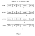
- the timing generator 7 calculates the current timing within the respective slots by means of the counter 72 on the basis of the slot boundary timing information and the slot format information shown in FIG. 4. Then, referring to the table 73, the AGC gain update timing is outputted from the controller 71, for example, at timings t1 to t4 shown in FIG. 5 (first to fourth positions) for each of the slots.
- the table 73 stores therein the information of the respective timing positions (t1 to t4) with reference to the slot boundary for each of the slots, as shown in FIG. 5.
- the counter 72 starts to count up the clocks with the slot boundary as a trigger, and when the count value coincides with the information of the storage timing positions corresponding to the slot formats (for example, slot No.), respectively, the controller 71 outputs the slot AGC update timing signal at that time.
- the reason that the AGC gain update timing is shifted for each of the slots is to prevent the update of the AGC gain from being conducted at the symbol position of the same W-CDMA (Wideband-CDMA) in each slot. Accordingly, the amount of shift of the AGC gain update timing for each of the slots is required to be larger than a period corresponding to one symbol.
- the shift of the respective AGC gain update timings by the symbol unit in the above manner can be readily realized by using the table 73 combining the slot format information and the AGC gain update timing as described above.
- the AGC gain update timing can be absorbed in a period indicated as "update timing in waiting” as shown in FIG. 6.
- FIG. 6 shows a relationship of a period of "update timing in waiting", a period of "power calculation”, and a period of "gain calculation”.
- the AGC gain update timing is set as a data portion (DPDCH) in each of the slots.
- DPDCH data portion
- the DPCCH is not subjected to error correcting, and weak in disturbance.
- the DPDCH portion is subjected to convolutional codes correcting on a slot format basis.
- the instability period occurs at a specific position of the slot format (that is, the same position in each of the slots) due to the AGC gain update each time, the characteristics are remarkably deteriorated.
- the AGC gain update timing occurs only at the DPDCH portion where the error correcting is conducted.
- the timing is shifted for each slot by a period longer than the one-symbol corresponding period under the control.
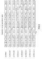
- FIG. 7 is a diagram showing another example of the transition of the AGC gain update timing.
- the AGC gain update timing is shifted only at the portion of data 2 of the DPDCH.
- the AGC gain update timing is shifted only at the portion of data 1 and data 2 of the DPDCH.
- FIGS. 8 to 10 are diagrams showing a third, a fourth and a fifth examples of the transition of the AGC gain update timing, respectively.
- the AGC gain update timing is shifted for each of the slots, respectively.
- FIG. 8 (t1 to t8) and FIG. 9 (t1 to t10) the AGC gain update timing is shifted for every two slots, respectively.
- the present invention is not limited to every slot or every two slots.
- the AGC gain update timing may be shifted for every 15 slots that constitute one frame, respectively.
- a period between one AGC gain update timing and a subsequent update timing is set to a period longer than one slot.
- the period is shorter than one slot.
- the control of the AGC gain update timing can be variously modified.
- the timing generator 7 shown in FIG. 1 may be constituted by hardware as shown in FIG. 3.
- operating procedures may naturally be recorded in a ROM (read only memory) or the like as a program, and read by a CPU (computer) for execution thereof.
Landscapes
- Circuits Of Receivers In General (AREA)
- Control Of Amplification And Gain Control (AREA)
Abstract
Description
- The present invention relates to an AGC (automatic gain control) system, an AGC method, and a receiver using the AGC system. In particular, the present invention relates to an AGC system in a receiver of a CDMA (code division multiple access) system and a direct conversion system.
- In recent years, with the spread of a mobile phone and other wireless portable terminals, demands for downsized wireless devices, lower power consumption, and lower prices have been increasingly made. As one of wireless receiving systems that meets the above demands, there is a direct conversion system. The direct conversion system converts a received radio frequency (RF) signal into a baseband signal. In the case where the direct conversion system is used in a receiver of a wireless device that operates with a low power as with a mobile phone, it is important to remove a direct current (DC) offset voltage. The removal of the direct current offset component specific to the direct conversion system is disclosed in "Baseband circuit in a direct conversion receiver" of JP 2002-111764 A (laid open in April 12, 2002).
- For removing the direct offset component,the baseband circuit disclosed in the above-mentioned JP 2002-111764 A uses a filter; however, it needs a time attributable to a time constant of the filter for stabilizing the filter. Accordingly, there occurs an instability period of a received signal, that is, a noise generation period. It is necessary to suppress an influence of the instability period (noise generation period) on the signal as much as possible.
- In general, in the receiver, it is necessary to change over the gain of an amplifier by using the AGC system. The amplifier connects to the filter of the receiver, and amplifies the baseband signal. When the gain is changed over, the function of removing the direct offset component is operated, and the above instability period occurs. In particular, in the DS-CDMA (direct sequence-code division multiple access)-based communication system, data is subjected to band spreading by a broadband spreading code. Accordingly, because the information is always transmitted, there is no temporal gap in received RF signal. As a result, the above instability period of the received signal leads to the deterioration of the receiving performance.
- In addition, when the instable receiving state occurs at the same timing within a slot cyclically or at a specific position by a time slot (hereinafter referred to simply as "slot") of the received signal, the receiving performance is remarkably deteriorated.
- The present invention has been made in view of the above, and therefore an object of the present invention is to provide a direct conversion receiver and an AGC (automatic gain control) system which suppresses an influence of the instability period of the received signal which is attributable to the gain update timing of the AGC on the received signal as much as possible.
- According to an aspect of the present invention, there is provided an AGC system which is used in a receiver of a direct conversion system, including controller for controlling an AGC gain update timing in a slot format of a received signal.
- The controller may generate a first AGC gain update timing at a first position within one slot of the received signal, and may generate a second AGC gain update timing subsequent to the first AGC gain update timing at a second position different from the first position within another slot.
- Further, when each of the slots of the received signal includes a first information portion having a predetermined code correcting capability and a second information portion having a code correcting capability smaller than the predetermined code correcting capability, the controller may generate the AGC gain update timing at the first information portion. Further, the received signal has a slot format of a CDMA system, and the amount of shift of the AGC gain update timing is preferably set to be larger than a period corresponding to one reception symbol of the CDMA system.
- According to another aspect of the present invention, there is provided an AGC system in a receiver of a direct conversion system, including a control step for controlling an AGC gain update timing in a slot format of a received signal.
- Further, the control step may include generating a first AGC gain update timing at a first position within one slot of the received signal, and generating a second AGC gain update timing subsequent to the first AGC gain update timing at a second position different from the first position within another slot.
- According to another aspect of the present invention, there is provided a program for causing a computer to execute an AGC method in a receiver of a direct conversion system, having a control process for controlling shift of an AGC gain update timing in a slot format of a received signal.
- The following are operations of the present invention. That is, in a slot format of a received signal, AGC gain update timings are shifted every time to disperse and reduce an influence of a noise attributable to a direct current component specific to direct conversion which is accompanied by AGC gain update. In particular, in the case where each of slots in the received signal includes an information portion having a larger code correcting capability and an information portion having a smaller code correcting capability (CDMA system), the AGC gain update timing is generated while being shifted in the information portion having a larger code correcting capability, thereby reduce the influence of the noise. Also, since the amount of shift of the AGC gain update timing is made larger than one symbol of the received signal, an influence of the noises accompanied by the AGC gain update is further reduced.
- According to the present invention, the timing of setting the AGC gain is shifted in the slot format of the received signal each time, so that a portion where there occurs the instability period of the received signal due to the direct-current component specific to the direct conversion system, is shifted. An influence of the instability period on the received signal can be reduced as much as possible, thereby making it possible to improve the error rate of the signal.
- These and other aspects, features and advantages of the invention will become more fully apparent from the following detailed description taken in conjunction with accompanying drawings. In the drawings:
- FIG. 1 is a block diagram showing an embodiment according to the present invention;
- FIG. 2 is a flowchart showing an operation of the embodiment according to the present invention;
- FIG. 3 is a block diagram showing functions of a timing generator shown in FIG. 1;
- FIG. 4 is a diagram showing a slot and frame format of a down-link DPCH regulated by 3GPP (third generation partnership project);
- FIG. 5 is a diagram showing a first example of transition of an AGC gain update timing;
- FIG. 6 is a diagram showing an AGC gain update timing adjusted position;
- FIG. 7 is a diagram showing a second example of transition of the AGC gain update timing;
- FIG. 8 is a diagram showing a third example of transition of the AGC gain update timing;
- FIG. 9 is a diagram showing a fourth example of transition of the AGC gain update timing; and
- FIG. 10 is a diagram showing a fifth example of transition of the AGC gain update timing.
-
- Hereinafter, a description will be given in more detail of preferred embodiments of the present invention with reference to the accompanying drawings. FIG. 1 is a block diagram showing an embodiment of the present invention. Referring to FIG. 1, a received radio signal is inputted from an
antenna 1 to adirect conversion receiver 2. Thedirect conversion receiver 2 includes a radio frequency amplifier (RF amplifier) 21,quadrature mixers local oscillator 23, a 90-degree phase shifter 24, LPFs (low-pass filters) 25a and 25b,baseband amplifiers gain controller 27. The operation of thedirect conversion receiver 2 has been disclosed in detail in "Direct conversion receiver" of JP 10-308684 A (laid open in November 17, 1998), and well known, and therefore its description will be omitted. - IQ signals (I data, Q data) that have been outputted from the
direct conversion receiver 2 are supplied to A/D (analog-to-digital)converters power calculator 4 for AGC. A power value calculated by thepower calculator 4 is supplied to anAGC gain calculator 5. TheAGC gain calculator 5 calculates the AGC gain of the amplifier in thedirect conversion receiver 2. - The AGC gain thus calculated is latched by a
gain latch circuit 6. Thegain latch circuit 6 latches the gain value until an AGC gain update timing signal is inputted to thegain latch circuit 6 from atiming generator 7. Upon receiving the AGC gain update timing signal from thetiming generator 7, thegain latch circuit 6 outputs the latchedAGC gain to thegain controller 27 of thedirect conversion receiver 2 at that timing. In this manner, the AGC gain is updated. - FIG. 2 is a flowchart showing the operation of the embodiment according to the present invention. The
power calculator 4 calculates a received power (Step S1). TheAGC gain calculator 5 calculates theAGC gain of thedirect conversion receiver 2 on the basis of a difference between the calculated received power value and a convergence target of AGC (Step S2). The AGC gain thus obtained is latched and temporarily held by thegain latch circuit 6. - Then, in the
timing generator 7, it is judged whether the update timing of the AGC gain is reached or not (Step S4). If the update timing is reached, the AGC gain update timing signal is generated from thetiming generator 7, and the latched AGC gain is read from thegain latch circuit 6. In this manner; the AGC gain is updated (Step S5). After the AGC gain has been updated, the operation is again returned to Step S1, and the same operation is repeated. - FIG. 3 is a block diagram showing the functions of the
timing generator 7 in FIG. 1. Thetiming generator 7 has acontroller 71, acounter 72, and a table 73 for AGC gain update timing generation. Thecontroller 71 inputs received signal slot format information and slot boundary timing information from a digital signal processor (not shown). Thecontroller 71 controls thecounter 72 and the table 73 on the basis of the inputted information. The counter 72 counts clocks in synchronism with the received data with the slot boundary timing information as a trigger. Accordingly, the output of thecounter 72 represents the present timing position within the respective slots. - In this example, the table 73 is a table that combines the respective slot format information of the received signal with the AGC gain update timing information,. The
controller 71 reads the AGC gain update timing for each of the slots from the table 73 on the basis of the inputted slot format information and the current timing position information within the respective slots of thecounter 72, and derives the read timing as the AGC gain update timing. - FIG. 4 shows a slot and frame format of a down-link'DPCH (dedicated physical channel) regulated by 3GPP (Third Generation Partnership Project). One frame of the down-link DPCH consists of 15 slots, and each of the slots consists of a DPDCH (dedicated physical data channel) and a DPCCH (dedicated physical control channel). The DPDCH consists of
data 1 and data 2.The DPCCH consists of a TPC (transmission power control) that is power control information, a TFCI (transport format combination indicator) that is feedback information, and a pilot that is a pilot signal. - Also, the slot format information is information indicative of the slot format shown in FIG. 4. The slot boundary timing information is information indicative of the slot boundary position.
- Accordingly, the
timing generator 7 calculates the current timing within the respective slots by means of thecounter 72 on the basis of the slot boundary timing information and the slot format information shown in FIG. 4. Then, referring to the table 73, the AGC gain update timing is outputted from thecontroller 71, for example, at timings t1 to t4 shown in FIG. 5 (first to fourth positions) for each of the slots. - In'this case, the table 73 stores therein the information of the respective timing positions (t1 to t4) with reference to the slot boundary for each of the slots, as shown in FIG. 5. The counter 72 starts to count up the clocks with the slot boundary as a trigger, and when the count value coincides with the information of the storage timing positions corresponding to the slot formats (for example, slot No.), respectively, the
controller 71 outputs the slot AGC update timing signal at that time. - As shown in FIG. 5, the reason that the AGC gain update timing is shifted for each of the slots is to prevent the update of the AGC gain from being conducted at the symbol position of the same W-CDMA (Wideband-CDMA) in each slot. Accordingly, the amount of shift of the AGC gain update timing for each of the slots is required to be larger than a period corresponding to one symbol. Thus, the shift of the respective AGC gain update timings by the symbol unit in the above manner can be readily realized by using the table 73 combining the slot format information and the AGC gain update timing as described above.
- Also, the AGC gain update timing can be absorbed in a period indicated as "update timing in waiting" as shown in FIG. 6. FIG. 6 shows a relationship of a period of "update timing in waiting", a period of "power calculation", and a period of "gain calculation".
- As shown in FIG. 5, the AGC gain update timing is set as a data portion (DPDCH) in each of the slots. The reason is stated below. In the down-link DPCH applied to IMT-2000 (International Mobile Telecommunications 2000) of 3GPP (Third Generation Partnership Project), the DPCCH is not subjected to error correcting, and weak in disturbance. Also, the DPDCH portion is subjected to convolutional codes correcting on a slot format basis. In the case where the instability period occurs at a specific position of the slot format (that is, the same position in each of the slots) due to the AGC gain update each time, the characteristics are remarkably deteriorated. For that reason, the AGC gain update timing occurs only at the DPDCH portion where the error correcting is conducted. In addition, the timing is shifted for each slot by a period longer than the one-symbol corresponding period under the control.
- FIG. 7 is a diagram showing another example of the transition of the AGC gain update timing. In the example shown in FIG. 5, the AGC gain update timing is shifted only at the portion of
data 2 of the DPDCH. In the example shown in FIG. 7 (t1 to t5), the AGC gain update timing is shifted only at the portion ofdata 1 anddata 2 of the DPDCH. FIGS. 8 to 10 are diagrams showing a third, a fourth and a fifth examples of the transition of the AGC gain update timing, respectively. In the above examples shown in FIGS. 5 and 7, the AGC gain update timing is shifted for each of the slots, respectively. However, in FIG. 8 (t1 to t8) and FIG. 9 (t1 to t10), the AGC gain update timing is shifted for every two slots, respectively. The present invention is not limited to every slot or every two slots. For example, the AGC gain update timing may be shifted for every 15 slots that constitute one frame, respectively. - Also, in the examples of FIGS. 5 and 7, a period between one AGC gain update timing and a subsequent update timing is set to a period longer than one slot. However, in FIG. 10 (t1 to t5), the period is shorter than one slot. It is apparent that the control of the AGC gain update timing can be variously modified. In addition, the
timing generator 7 shown in FIG. 1 may be constituted by hardware as shown in FIG. 3. Alternatively, operating procedures may naturally be recorded in a ROM (read only memory) or the like as a program, and read by a CPU (computer) for execution thereof.
Claims (10)
- An AGC system which is used in a receiver of a direct conversion system, comprising
controller which controls an AGC gain update timing in a slot format of a received signal. - An AGC system according to claim 1, wherein the controller generates a first AGC gain update timing at a first position within one slot of the received signal, and generates a second AGC gain update timing subsequent to the first AGC gain update timing at a second position different from the first position within another slot.
- An AGC system according to claim 1, wherein:each of the slots of the received signal includes a first information portion having a predetermined code correcting capability and a second information portion having a code correcting capability smaller than the predetermined code correcting capability; andthe controller generates the AGC gain update timing at the first information portion.
- An AGC system according to claim 1, wherein:the received signal has a slot format of a CDMA system; and the amount of shift of the AGC gain update timing is set to be larger than a period corresponding to one reception symbol of the CDMA system.
- A receiver which has the AGC system according to claim 1.
- An AGC method which is used in a receiver of a direct conversion system, comprising
a control step for controlling an AGC gain update timing in a slot format of a received signal. - An AGC method according to claim 6, wherein the control step comprises:generating a first AGC gain update timing at a first position within one slot of the received signal; andgenerating a second AGC gain update timing subsequent to the first AGC gain update timing at a second position different from the first position within another slot.
- An AGC method according to claim 6, wherein:each of the slots of the received signal includes a first information portion having a predetermined code correcting capability and a second information portion having a code correcting capability smaller than the predetermined code correcting capability; andthe control step comprises generating the AGC gain update timing at the first information portion.
- An AGC method according to claim 6, wherein:the received signal has a slot format of a CDMA system; andthe amount of shift of the AGC gain update timing is set to be larger than a period corresponding to one reception symbol of the CDMA system.
- A program for causing a computer to execute an AGC method in a receiver of a direct conversion system, comprising
a control process for controlling shift of an AGC gain update timing in a slot format of a received signal.
Applications Claiming Priority (2)
| Application Number | Priority Date | Filing Date | Title |
|---|---|---|---|
| JP2003411131A JP4419545B2 (en) | 2003-12-10 | 2003-12-10 | AGC control system, control method therefor, and receiver using the same |
| JP2003411131 | 2003-12-10 |
Publications (1)
| Publication Number | Publication Date |
|---|---|
| EP1542358A1 true EP1542358A1 (en) | 2005-06-15 |
Family
ID=34510507
Family Applications (1)
| Application Number | Title | Priority Date | Filing Date |
|---|---|---|---|
| EP20040029197 Withdrawn EP1542358A1 (en) | 2003-12-10 | 2004-12-09 | AGC system, AGC method, and receiver using the AGC system |
Country Status (4)
| Country | Link |
|---|---|
| US (1) | US7496163B2 (en) |
| EP (1) | EP1542358A1 (en) |
| JP (1) | JP4419545B2 (en) |
| CN (1) | CN1627634B (en) |
Cited By (2)
| Publication number | Priority date | Publication date | Assignee | Title |
|---|---|---|---|---|
| WO2009093154A1 (en) * | 2008-01-22 | 2009-07-30 | Nxp B.V. | Automatic gain control in a radio receiver circuit, and related interface |
| EP1916766A3 (en) * | 2006-10-25 | 2010-09-15 | EADS Deutschland GmbH | Voltage regulator |
Families Citing this family (11)
| Publication number | Priority date | Publication date | Assignee | Title |
|---|---|---|---|---|
| US7596193B2 (en) | 2005-11-09 | 2009-09-29 | Via Telecom, Inc. | Variable bandwidth automatic gain control |
| US7953191B2 (en) * | 2005-12-28 | 2011-05-31 | Thomson Licensing | Gain control method and device for a bursty data frame reception system |
| JP2007281633A (en) * | 2006-04-04 | 2007-10-25 | Niigata Seimitsu Kk | Receiving machine |
| US7978773B2 (en) * | 2006-12-29 | 2011-07-12 | Agere Systems Inc. | Multi-channel receiver with improved AGC |
| US7769357B2 (en) * | 2007-04-25 | 2010-08-03 | Agere Systems Inc. | Multi-channel receiver with improved AGC |
| US7809343B2 (en) | 2007-04-25 | 2010-10-05 | Agere Systems Inc. | Multi-channel receiver with improved AGC |
| US8634766B2 (en) | 2010-02-16 | 2014-01-21 | Andrew Llc | Gain measurement and monitoring for wireless communication systems |
| TWI418143B (en) * | 2010-08-26 | 2013-12-01 | Global Unichip Corp | Communication apparatus having automatic gain control device and automatic gain control method |
| DE102015106201A1 (en) * | 2015-04-22 | 2016-10-27 | Intel IP Corporation | CIRCUIT, INTEGRATED CIRCUIT, RECEIVER, TRANSMIT RECEIVER, AND METHOD FOR RECEIVING A SIGNAL |
| KR102494784B1 (en) | 2015-07-28 | 2023-02-01 | 삼성전자주식회사 | Receiver and operating method thereof |
| CN109120292B (en) * | 2018-08-06 | 2019-11-05 | 电子科技大学 | A kind of digital automatic gain control system and method |
Citations (3)
| Publication number | Priority date | Publication date | Assignee | Title |
|---|---|---|---|---|
| US20030064696A1 (en) * | 2001-09-28 | 2003-04-03 | Yukinori Akamine | Wireless communication receiver |
| EP1324504A2 (en) * | 2001-12-25 | 2003-07-02 | Kabushiki Kaisha Toshiba | Radio receiver and radio receiving method |
| US20030207674A1 (en) * | 2000-06-01 | 2003-11-06 | Hughes James David | Method and apparatus for reducing intermodulation distortion in a low current drain automatic gain control system |
Family Cites Families (5)
| Publication number | Priority date | Publication date | Assignee | Title |
|---|---|---|---|---|
| JPH056943U (en) * | 1991-02-28 | 1993-01-29 | 株式会社東芝 | Gain control circuit |
| JP3489621B2 (en) | 2000-09-28 | 2004-01-26 | 日本電気株式会社 | Baseband circuit of direct conversion receiver |
| WO2003021765A1 (en) * | 2001-08-29 | 2003-03-13 | Seiko Epson Corporation | Oscillator and communication appliance |
| JP2003092561A (en) * | 2001-09-18 | 2003-03-28 | Sony Corp | Receiving device and receiving method |
| US6873833B2 (en) * | 2003-03-27 | 2005-03-29 | Interdigital Technology Corporation | Method and apparatus for estimating and controlling initial time slot gain in a wireless communication system |
-
2003
- 2003-12-10 JP JP2003411131A patent/JP4419545B2/en not_active Expired - Fee Related
-
2004
- 2004-12-09 EP EP20040029197 patent/EP1542358A1/en not_active Withdrawn
- 2004-12-09 US US11/007,159 patent/US7496163B2/en not_active Expired - Fee Related
- 2004-12-10 CN CN2004100866602A patent/CN1627634B/en not_active Expired - Fee Related
Patent Citations (3)
| Publication number | Priority date | Publication date | Assignee | Title |
|---|---|---|---|---|
| US20030207674A1 (en) * | 2000-06-01 | 2003-11-06 | Hughes James David | Method and apparatus for reducing intermodulation distortion in a low current drain automatic gain control system |
| US20030064696A1 (en) * | 2001-09-28 | 2003-04-03 | Yukinori Akamine | Wireless communication receiver |
| EP1324504A2 (en) * | 2001-12-25 | 2003-07-02 | Kabushiki Kaisha Toshiba | Radio receiver and radio receiving method |
Cited By (2)
| Publication number | Priority date | Publication date | Assignee | Title |
|---|---|---|---|---|
| EP1916766A3 (en) * | 2006-10-25 | 2010-09-15 | EADS Deutschland GmbH | Voltage regulator |
| WO2009093154A1 (en) * | 2008-01-22 | 2009-07-30 | Nxp B.V. | Automatic gain control in a radio receiver circuit, and related interface |
Also Published As
| Publication number | Publication date |
|---|---|
| CN1627634B (en) | 2011-06-15 |
| CN1627634A (en) | 2005-06-15 |
| US20050129150A1 (en) | 2005-06-16 |
| US7496163B2 (en) | 2009-02-24 |
| JP4419545B2 (en) | 2010-02-24 |
| JP2005175731A (en) | 2005-06-30 |
Similar Documents
| Publication | Publication Date | Title |
|---|---|---|
| JP4236587B2 (en) | Frequency timing control loop for wireless communication system | |
| US6941112B2 (en) | Gain control amplification circuit and terminal equipment having the same | |
| KR100312580B1 (en) | Received power calculating method and mobile station | |
| KR100532266B1 (en) | Direct conversion receiver and dc offset reducing method | |
| US8233859B2 (en) | Apparatus and method for accurate and efficient transmit power control | |
| US7496163B2 (en) | AGC system, AGC method, and receiver using the AGC system | |
| JP2001223637A (en) | Wireless communication device and transmission power control method | |
| EP1061643B1 (en) | Receiver and gain control method of the same | |
| TW200931813A (en) | ADC use with multiple signal modes | |
| JP2008535377A (en) | DC offset correction system for a receiver with baseband gain control | |
| US9392551B2 (en) | Apparatus and method for matching antenna impedance in wireless communication system | |
| CN100495941C (en) | Noise gain control device and method | |
| US6832098B1 (en) | Portable telephone | |
| JP2004208180A (en) | Wireless communication device | |
| JP2002261638A (en) | Receiver for AGC control | |
| JP5396874B2 (en) | Terminal device, transmission power control method, and digital signal processing device | |
| JP2004363743A (en) | Wireless communication device | |
| JP4760241B2 (en) | Portable radio terminal, method for coping with interference wave, and control program | |
| JP3667240B2 (en) | Automatic gain control device for CDMA receiver | |
| JP5098811B2 (en) | Portable terminal device and power consumption control method thereof | |
| JP2006165677A (en) | Mobile radio terminal and receiving circuit | |
| JP4089413B2 (en) | Wireless communication apparatus and automatic gain control method used therefor | |
| JP2009267653A (en) | Radio communication device, and method for controlling transmission power | |
| JP2004221663A (en) | Wireless communication device | |
| JP2007174101A (en) | Digital signal receiver |
Legal Events
| Date | Code | Title | Description |
|---|---|---|---|
| PUAI | Public reference made under article 153(3) epc to a published international application that has entered the european phase |
Free format text: ORIGINAL CODE: 0009012 |
|
| AK | Designated contracting states |
Kind code of ref document: A1 Designated state(s): AT BE BG CH CY CZ DE DK EE ES FI FR GB GR HU IE IS IT LI LT LU MC NL PL PT RO SE SI SK TR |
|
| AX | Request for extension of the european patent |
Extension state: AL BA HR LV MK YU |
|
| 17P | Request for examination filed |
Effective date: 20050421 |
|
| AKX | Designation fees paid |
Designated state(s): DE FR GB IT |
|
| 17Q | First examination report despatched |
Effective date: 20050809 |
|
| STAA | Information on the status of an ep patent application or granted ep patent |
Free format text: STATUS: THE APPLICATION HAS BEEN WITHDRAWN |
|
| 18W | Application withdrawn |
Effective date: 20061129 |