EP1542311A1 - Control device and control method - Google Patents
Control device and control method Download PDFInfo
- Publication number
- EP1542311A1 EP1542311A1 EP02775471A EP02775471A EP1542311A1 EP 1542311 A1 EP1542311 A1 EP 1542311A1 EP 02775471 A EP02775471 A EP 02775471A EP 02775471 A EP02775471 A EP 02775471A EP 1542311 A1 EP1542311 A1 EP 1542311A1
- Authority
- EP
- European Patent Office
- Prior art keywords
- components
- impedance
- evaluation function
- control unit
- function value
- Prior art date
- Legal status (The legal status is an assumption and is not a legal conclusion. Google has not performed a legal analysis and makes no representation as to the accuracy of the status listed.)
- Withdrawn
Links
Images



Classifications
-
- H—ELECTRICITY
- H01—ELECTRIC ELEMENTS
- H01Q—ANTENNAS, i.e. RADIO AERIALS
- H01Q3/00—Arrangements for changing or varying the orientation or the shape of the directional pattern of the waves radiated from an antenna or antenna system
- H01Q3/26—Arrangements for changing or varying the orientation or the shape of the directional pattern of the waves radiated from an antenna or antenna system varying the relative phase or relative amplitude of energisation between two or more active radiating elements; varying the distribution of energy across a radiating aperture
-
- H—ELECTRICITY
- H01—ELECTRIC ELEMENTS
- H01Q—ANTENNAS, i.e. RADIO AERIALS
- H01Q3/00—Arrangements for changing or varying the orientation or the shape of the directional pattern of the waves radiated from an antenna or antenna system
- H01Q3/26—Arrangements for changing or varying the orientation or the shape of the directional pattern of the waves radiated from an antenna or antenna system varying the relative phase or relative amplitude of energisation between two or more active radiating elements; varying the distribution of energy across a radiating aperture
- H01Q3/2605—Array of radiating elements provided with a feedback control over the element weights, e.g. adaptive arrays
-
- H—ELECTRICITY
- H01—ELECTRIC ELEMENTS
- H01Q—ANTENNAS, i.e. RADIO AERIALS
- H01Q3/00—Arrangements for changing or varying the orientation or the shape of the directional pattern of the waves radiated from an antenna or antenna system
- H01Q3/26—Arrangements for changing or varying the orientation or the shape of the directional pattern of the waves radiated from an antenna or antenna system varying the relative phase or relative amplitude of energisation between two or more active radiating elements; varying the distribution of energy across a radiating aperture
- H01Q3/30—Arrangements for changing or varying the orientation or the shape of the directional pattern of the waves radiated from an antenna or antenna system varying the relative phase or relative amplitude of energisation between two or more active radiating elements; varying the distribution of energy across a radiating aperture varying the relative phase between the radiating elements of an array
- H01Q3/34—Arrangements for changing or varying the orientation or the shape of the directional pattern of the waves radiated from an antenna or antenna system varying the relative phase or relative amplitude of energisation between two or more active radiating elements; varying the distribution of energy across a radiating aperture varying the relative phase between the radiating elements of an array by electrical means
- H01Q3/36—Arrangements for changing or varying the orientation or the shape of the directional pattern of the waves radiated from an antenna or antenna system varying the relative phase or relative amplitude of energisation between two or more active radiating elements; varying the distribution of energy across a radiating aperture varying the relative phase between the radiating elements of an array by electrical means with variable phase-shifters
-
- H—ELECTRICITY
- H01—ELECTRIC ELEMENTS
- H01Q—ANTENNAS, i.e. RADIO AERIALS
- H01Q9/00—Electrically-short antennas having dimensions not more than twice the operating wavelength and consisting of conductive active radiating elements
- H01Q9/04—Resonant antennas
- H01Q9/0407—Substantially flat resonant element parallel to ground plane, e.g. patch antenna
- H01Q9/0442—Substantially flat resonant element parallel to ground plane, e.g. patch antenna with particular tuning means
-
- H—ELECTRICITY
- H04—ELECTRIC COMMUNICATION TECHNIQUE
- H04B—TRANSMISSION
- H04B1/00—Details of transmission systems, not covered by a single one of groups H04B3/00 - H04B13/00; Details of transmission systems not characterised by the medium used for transmission
- H04B1/06—Receivers
- H04B1/16—Circuits
- H04B1/18—Input circuits, e.g. for coupling to an antenna or a transmission line
Definitions
- the present invention generally relates to a control unit and a control method of appropriately maintaining an output signal of a nonlinear system by carrying out adaptive control of variable impedance components, and especially relates to a control unit and a control method of appropriately maintaining a signal received by an adaptive antenna system that has two or more antenna elements.
- appropriately maintaining an output signal is often carried out by optimizing impedance by an optimization technique that uses a perturbation method in a nonlinear system wherein an output signal changes depending on the impedance of two or more components.
- Fig. 1 is a conceptual diagram showing an example of a conventional control system 100.
- the control system 100 serves a radio frequency (RF) processing type adaptive antenna system, and is a nonlinear system wherein the impedances of two or more RF components (L, C) are unknown, and two or more received signals are added and output.
- the control system 100 includes two or more antenna elements 102, the quantity of which is expressed as M+1, and an adder 104 that combines signals from the antenna elements 102.
- the output of the adder 104 is provided to an analog-to-digital converter 106.
- the output of the analog-to-digital converter 106 is provided to a control unit 108.
- the inductance of the inductor L i and the capacitance of the capacitor C i are adjusted by a control signal provided by the control unit 108.
- Fig. 2 is a flowchart showing a control flow 200 of the control system 100 mainly performed by the control unit 108, the control flow 200 employing the perturbation method.
- the control flow 200 starts at Step 202.
- impedance x i of two or more components is set at a suitable initial value.
- a parameter m relevant to the number of repetition times of the process is set at an initial value 0.
- the evaluation function value is stored as a fiducial point f 0 (x).
- Step 210 the parameter m is incremented by one.
- the value of the impedance x m of the m-th component is changed to x m + ⁇ x m .
- x m the value of the impedance x m of the m-th component
- a minute change is added to the value of the inductor L 1 .
- the minute change causes the output signal y(x) to change.
- the evaluation function value f(x) is calculated based on the output signal y(x).
- a slope (gradient) vector ⁇ f is calculated by computing the difference between the evaluation function values f(x) before and after the minute change of the impedance x m .
- Step 218 the added minute change ⁇ x m is deducted, and the value of x m returns to the original value.
- Step 220 it is determined whether the parameter m is equal to or less than 2M. If the determination is affirmative, the process returns to Step 208, and other components of the gradient vector ⁇ f are calculated. Otherwise, if m is determined to be greater than 2M, all the components of the gradient vector ⁇ f have been calculated.
- the impedance value x i is updated using the calculated gradient vector ⁇ f.
- the gradient vector ⁇ f represents the direction in which a slope (inclination) changes most rapidly in the coordinate (x 1 , x 2 , ..., x 2M ) of the curved surface expressed by f. That is, the maximum or the minimum value (the desired optimal value) of the evaluation function value f is present in the direction indicated by ⁇ f. Accordingly, the impedance value x is updated to x+ ⁇ f, where ⁇ represents a step size in the direction of ⁇ f.
- Step 224 it is determined whether the impedance value is satisfactorily converged by comparing the impedance value with the previous impedance value. If negative, the process returns to Step 206 for further updating. If affirmative, the process proceeds to Step 226, and the control flow 200 is ended.
- variable impedance component such as a variable inductor and a variable capacitor.
- the common practice is advantageous in that a high response speed is available when changing the impedance, a disadvantage is that high power is consumed. This is particularly disadvantageous for a small appliance that uses a battery.
- an impedance variable component is available, wherein the impedance is mechanically changed using a micro electro mechanical system (MEMS).
- MEMS micro electro mechanical system
- the impedance can be changed by various methods, and examples are to change the impedance by changing the interval between two plates of a capacitor, and by changing the amount of insertion of a magnetic core of an inductor.
- the MEMS type component consumes very little power, compared with the semiconductor integrated circuit, and it is possible to solve the problem concerning power consumption.
- the response time of the MEMS component tends to be longer than the semiconductor integrated circuit for the same impedance.
- the slow response poses a problem in that the gradient vector ⁇ f cannot be promptly calculated. That is, an MEMS type component is not capable of accurately following changes in a nonlinear system.
- a general objective of the present invention is to offer a control unit and a control method that provide a high-speed control of the impedance of two or more components that affect an output signal of a nonlinear system such that the output signal is maintained at a satisfactory level.
- a specific objective of the present invention is to offer a control unit and a control method that provide a low-power-consumption and high-speed control of the impedance of two or more components that affect an output signal of a nonlinear system such that the output signal is maintained at a satisfactory level.
- the present invention provides:
- Fig. 1 is a block diagram of an example of a conventional control system.
- Fig. 2 is a control flowchart performed by the conventional control system.
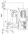
- Fig. 3 is a block diagram of an example of a control system according to the first embodiment of the present invention.
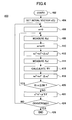
- Fig. 4 is a control flowchart performed by the control system according to the embodiment of the present invention.
- Fig. 5 is a block diagram of the control system according to the second embodiment of the present invention.
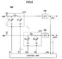
- Fig. 6 is a block diagram of the control system according to the third embodiment of the present invention.
- Fig. 3 is a block diagram showing an example of a control system 300 according to the first embodiment of the present invention.
- the control system 300 serves as a radio frequency (RF) processing type adaptive antenna system, and is a nonlinear system wherein impedances of two or more RF components are unknown, and two or more received signals are combined to form an output signal.
- the control system 300 includes antenna elements 302, the quantity of which is M+1, and an adder 304 configured to add the signals received by the M+1 antenna elements 302.
- the output of the adder 304 is provided to an analog-to-digital converter 306.
- the output of the analog-to-digital converter 306 is provided to a control unit 308.
- the phase shift circuit 310 consists of a first inductor L i 1 and a second inductor L i 2 connected in series to the antenna element 302, and a first capacitor C i 1 and a second capacitor C i 2 connected in parallel.
- i 1, ..., M.
- the first and the second inductors L i 1 and L i 2 , and the first and the second capacitors C i 1 and C i 2 are MEMS (micro electro mechanical system) components, the impedance of which is mechanically variable.
- a semiconductor device can serve as the components, the MEMS components are used in order to reduce power consumption.
- the inductance of the first and the second inductor L i 1 and L i 2 , and the capacitance of the first and second capacitors C i 1 and C i 2 , respectively, are adjusted by a control signal from the control unit 308.
- control signal x i 1 controls the first components, namely, the first inductor L i 1 and the first capacitor C i 1
- control signal x i 2 controls the second components, namely, the second inductor L i 2 and the second capacitor C i 2 .
- the inductance of the first inductor L i 1 and the capacitance of the first capacitor C i 1 are greatly changeable such that a magnitude of impedance (inductance/capacitance) change is great enough to optimize the property of the output signal (output signal from the digital-to-analog converter 306) of the nonlinear system. For this reason, the sizes of the first inductor L i 1 and the capacitance of the first capacitor C i 1 are relatively great, and their response speeds tend to be comparatively low.
- the second inductor L i 2 and the second capacitor C i 2 are of small size, and are capable of varying the respective impedance in a small range. Accordingly, the response speeds of the second inductor L i 2 and the second capacitor C i 2 are higher than the response speeds of the first inductor L i 1 and the first capacitor C i 1 , respectively.
- the control unit 308 of the adaptive antenna system 300 includes an evaluation function value calculating unit 311 configured to calculate an evaluation function value f(x) based on a signal y(x) output by the analog-to-digital converter 306.
- the evaluation function value f(x) various values can be used, such as a correlation value
- a signal-to-noise ratio and a signal-to-noise interference ratio may be used as the evaluation function value f(x).
- the evaluation function value f(x) any quantity that varies with changes of the impedance x, and that is available for optimizing the output signal (received signal y(x)) of the nonlinear system can be used.
- the control unit 308 includes a gradient vector calculating unit 312, to which the output signal of the evaluation function value calculating unit 311 is provided.
- the gradient vector calculating unit 312 calculates a slope ⁇ f of the evaluation function value f at the impedance vector x by computing the difference between the evaluation function values f(x) before and after the change of the impedance vector x.
- the output of the gradient vector calculating unit 312 is provided to a changing unit 314 that is configured to change the impedance value.
- the changing unit 314 includes a first changing unit 316 configured to change the inductance of the first inductor L i 1 and the capacitance of the first capacitor C i 1 change.
- the changing unit 314 includes a second changing unit 318 configured to change the inductance of the second inductor L i 2 and the capacitance of the second capacitor C i 2 . It should be noted that the amount of impedance change by the second changing unit 318 is very small as described above.
- the changing unit 314 further includes a digital-to-analog converter 320 configured to convert digital signals from the first and the second changing units 316 and 318 into analog signals, and to provide the control signals x i 1 and x i 2 to the first and the second inductors L i 1 and L i 2 , respectively, and to the first and the second capacitors C i 1 and C i 2 , respectively.
- the digital-to-analog converter 320 can be configured to serve both the first component and the second component; or alternatively, separate digital-to-analog converters may be provided to separately serve the first and the second components. When the digital-to-analog converter 320 serves both, a switch is provided.
- Fig. 4 shows a control flow 400 based on the perturbation method performed by the control unit 308 of the present embodiment.
- the control flow 400 starts at Step 402.
- impedance x i of the first and the second components are set at a suitable initial value.
- the value of a parameter m relevant to the number of process repetitions is set at an initial value 0.
- the evaluation function value f(x) is calculated by the evaluation function value calculating unit 311, and is stored as a fiducial point f 0 (x).
- Step 410 the value of the parameter m is incremented by one.
- the output signal y(x) changes by the minute impedance change ⁇ x m 2 .
- the evaluation function value f(x) is calculated based on the output signal y(x).
- the gradient vector ⁇ f is calculated by computing the difference between the evaluation function values f(x) before and after change of the impedance x m 2 of the second component.
- the gradient vector calculating unit 312 calculates the gradient vector ⁇ f.
- ⁇ f is a vector quantity that has 2M components, and each component is calculated by the following formula.
- xm f(x 1 1 , x 1 2 , ..., x m 1 , x m 2 + ⁇ x m 2 , ..., x 2M 1 , x 2M 2 )-f0(x 1 1 , x 1 2 , ..., x m 1 , x m 2 , ..., x 2M 1 , x 2M 2 )
- the second components (x i 2 ) are auxiliary impedance components prepared for the perturbation calculation at coordinates x 1 1 , x 2 1 , ..., x 2M 1 on an f-curved surface
- the number of components of the gradient vector ⁇ f is defined by the number of the first components, i.e., 2M.
- Step 418 the minute change is deducted such that the impedance value returns to the original value x m 2 .
- Step 420 whether the value of parameter m is equal to or less than 2M is determined. If affirmative, the process returns to Step 408, and other components of the gradient vector are calculated. Otherwise, i.e., if negative, and if the value of the parameter m is not equal to or less than 2M, it is determined that all the components of the gradient vector ⁇ f have been calculated.
- the gradient vector ⁇ f is calculated by changing the impedance of the second components L i 2 and C i 2 that are prepared in addition to the first components L i 1 and C i 1 .
- the variable impedance range of the second components is smaller than the first components, the response speed of the second components is high because the size is small.
- the addition at Step 410 and the subtraction at Step 418 of the minute change ⁇ x m 2 are carried out at a high speed. In this manner, the gradient vector ⁇ f is quickly obtained. That is, if the influence of the minute change of the impedance to the evaluation function is known, it is possible to obtain the gradient vector ⁇ f.
- the gradient vector ⁇ f is quickly obtained by providing the second components L i 2 and C i 2 , response of which is remarkably quick, in addition to the first components.
- a total inductance L i 0 is equal to L i 1 +L i 2 .
- the total inductance L i 0 is changed by the minute change at Step 412 to L i 1 +L i 2 + ⁇ L i 2 , which is equal to L i 0 + ⁇ L i 2 .
- a total capacitance C i 0 is equal to C i 1 +C i 2 .
- the total capacitance C i 0 is changed by the minute change at Step 412 to C i 1 +C i 2 + ⁇ C i 2 , which is equal to C i 0 + ⁇ C i 2 . Accordingly, the influence of the minute change of the inductor and/or the capacitor of the phase shift circuit 310 is detected for calculating the gradient vector.
- the impedance value x i 1 of the first component is updated using the gradient vector ⁇ f calculated based on the change due to the minute impedance change of the second-component.
- the gradient vector ⁇ f shows the direction in which the inclination changes the most rapidly at the points x 1 1 , x 2 1 , .., and x 2M 1 on the f-curved surface.
- the maximum or the minimum value (the desired optimal value) of the evaluation function value f is present in the direction that is given by ⁇ f.
- the parameter ⁇ represents a step size when following a pass along the direction indicated by ⁇ f when updating the impedance value x i 1 of the first component.
- Step 424 it is determined whether the impedance value is sufficiently converged by comparing it with the immediately previous impedance value. If the determination is negative, the process returns to Step 406 for further updating. If, otherwise, the determination is affirmative, the process proceeds to Step 426 and the control flow 400 is ended.
- the impedance control is carried out at a remarkably high speed.
- the process loop between Step 208 and Step 220 contains impedance value changes at Steps 210 and 220, which require a long time.
- the present invention changes the impedance of the second components L i 2 and C i 2 , response time of which is remarkably short; and therefore, the process loop between Steps 408 and 420 can be quickly performed. For example, if M is set at 10, there are 11 antenna elements, 10 inductors, and 10 capacitors, i.e., 20 components, impedances of which are adjusted.
- the loop that includes Step 212 and Step 218 for repeatedly calculating the gradient vector sequentially changes the impedance of the 20 components.
- a time required by this process is 20 x (10 ⁇ s + 10 ⁇ s).
- Step 222 is carried out 100 times
- the time required by Step 222 is 10 ⁇ s.
- the time required by steps other than Steps 212, 218, and 222 in the control flow 200 is omitted.
- the second components are small sized, and have a remarkably high response speed.
- the second components used by the present invention have a small impedance variable range, such as 1/512 of the first components; however, the response speed is as high as 51.2 MHz (i.e., 10 ⁇ s/512). (Here, for simplicity, the response speed is assumed to be in inverse-proportion to the variable range.) Accordingly, the time required to calculate the gradient vector ⁇ f by repeating the loop containing Step 412 and Step 418 20 times becomes (10 ⁇ s/512 + 10 ⁇ s/512) x 20.
- control unit and the control method according to the present invention embodiment realize a very high-speed control.
- the time required by steps other than Steps 412,418, and 422 in the control flow 400 is omitted.
- Fig. 5 is a block diagram of a control system 500 according to the second embodiment of the present invention.
- the control system 500 serves as a space processing type array antenna system, which is a nonlinear system with two or more antenna elements 502, of which the impedance of the RF component (C) is unknown, wherein a signal received by an antenna element 504 varies with changes of the impedance.
- the control system 500 includes M antenna elements 502, and the antenna element 504 that is connected to an analog-to-digital converter 506.
- the output of the analog-to-digital converter 506 is provided to a control unit 508 that is the same as the control unit 308 explained with reference to Fig. 3.
- Each of the M antenna elements 502 includes a first capacitor C i 1 that functions as the first component, and a second capacitor C i 2 that functions as the second component affecting the directivity of the array antenna.
- the control unit 508 controls the capacitance of the first and second capacitors C i 1 and C i 2 .
- the second embodiment is to maintain satisfactory signal reception by realizing a predetermined antenna directivity with the M+1 antenna elements spatially coupled.
- the antenna directivity formed by the antenna elements is adjusted such that a desired signal is best received by setting a main lobe to the direction of the desired wave, and setting a null point to an interference wave.
- the impedance of the first component is optimized by performing a control flow that is the same as described above with reference to Fig. 2.
- the second embodiment only the M first capacitors C i 1 that accompany M respective antennas, and the M second capacitors C i 2 for giving minute impedance change to the respective antenna elements are to be controlled. That is, the number of the components that are to be controlled is reduced, which is an advantage of the second embodiment, especially when applying the present invention to small apparatuses.
- Fig. 6 is a block diagram of a control system 600 according to the third embodiment of the present invention.
- the control system 600 serves as a digital processing type array antenna system, and includes antenna elements 602, each of which further includes a matching circuit 610 for taking impedance matching, and an analog-to-digital converter 606.
- the impedance of the first and the second component are adjusted based on control signals x i 1 and x i 2 , respectively, provided by a control unit 608.
- the evaluation function value f(x) is calculated based on the total of the signals received through each path of the antenna elements 602. Specifically, the evaluation function value f(x) is calculated by obtaining a power value by squaring the received signal y i (x) from each path, and totaling the power values. That is, according to the embodiment, a signal is appropriately received by adjusting matching of the impedance of each antenna element.
- the matching circuit 610 of the embodiment can be effectively used by the control system according to the first embodiment and the second embodiment.
- two or more second components x i 2 that affect the output signal of a nonlinear system are provided in addition to two or more first components x i 1 , the gradient vector ⁇ f is obtained using the second components, and the impedance of the first components is changed based on the gradient vector ⁇ f. Since the gradient vector ⁇ f can be obtained by providing a minute change of the impedance that affects the output signal, the size of the second components can be very small, which means that the second components have a high-speed response. That is, the gradient vector ⁇ f can be quickly obtained using the second components.
- the impedance of the first components is adjusted based on the quickly obtained gradient vector ⁇ f so as to obtain the maximum or the minimum output signal.
- an output signal is formed based on the high-frequency signals received by the antenna elements, and the first and the second components consist of capacitors and inductors.
- the mechanical component (MEMS) type capacitors and inductors is considered in an attempt to reduce power consumption as compared with semiconductor devices; however, the response speed of the MEMS type components is low, and it is difficult to employ the MEMS type components.
- the present invention uses small size MEMS type components as the second components for determining the gradient vector ⁇ f, a high-speed operation is realized. Accordingly, high-speed control of the first components is realized, and power consumption is reduced.
- the present invention is capable of setting up different magnitudes of the minute change ⁇ x m 2 for each of the antenna elements (that is, different antenna elements can take different minute changes).
- This feature makes the present invention applicable to various control systems.
- all the minute changes ⁇ x m 2 may be set at the same predetermined fixed value, in which case, the processing burden of the control system is mitigated, and a high-speed operation is obtained.
- the control system of the present invention can be applied to any system using two or more antenna elements such as a radio base station, a mobile terminal, and the like, especially where reduced power consumption is a requirement, e.g. a small portable apparatus.
- variable impedance components are used to form the phase shift circuit, the reactance circuit, and the matching circuit in the embodiments above, the present invention is not limited to such a form; but variable impedance components can form various circuits that are configured to affect an output signal.
- the present invention is described in relation to the antenna system, the present invention is not limited to such a form. Rather, the present invention can be widely applied to control systems wherein impedance of two or more components of a nonlinear system, where an output signal changes depending on the impedance, is optimized by the perturbation method.
- the impedances of two or more components that affect an output signal are controlled at a high speed in order to satisfactorily maintain the output signal of the nonlinear system.
Landscapes
- Engineering & Computer Science (AREA)
- Computer Networks & Wireless Communication (AREA)
- Signal Processing (AREA)
- Variable-Direction Aerials And Aerial Arrays (AREA)
- Details Of Aerials (AREA)
Abstract
A control unit and a control method are
disclosed. First and a second changing units (316
and 318) change impedances of two or more first and
second components within a predetermined first and
second ranges, respectively, the first and the
second components affecting an output signal. An
evaluation function value calculating unit (311)
calculates an evaluation function value that is
dependent on the impedances of the first and the
second components. A gradient vector calculating
unit (312) calculates a gradient vector based on the
difference between the evaluation function values
before and after the impedance change of the second
components. Based on the gradient vector, impedance
of each of the first components is changed such that
the evaluation function value takes a desired value.
Description
The present invention generally relates to
a control unit and a control method of appropriately
maintaining an output signal of a nonlinear system
by carrying out adaptive control of variable
impedance components, and especially relates to a
control unit and a control method of appropriately
maintaining a signal received by an adaptive antenna
system that has two or more antenna elements.
In the technical field, appropriately
maintaining an output signal is often carried out by
optimizing impedance by an optimization technique
that uses a perturbation method in a nonlinear
system wherein an output signal changes depending on
the impedance of two or more components.
Fig. 1 is a conceptual diagram showing an
example of a conventional control system 100. The
control system 100 serves a radio frequency (RF)
processing type adaptive antenna system, and is a
nonlinear system wherein the impedances of two or
more RF components (L, C) are unknown, and two or
more received signals are added and output. The
control system 100 includes two or more antenna
elements 102, the quantity of which is expressed as
M+1, and an adder 104 that combines signals from the
antenna elements 102. The output of the adder 104 is
provided to an analog-to-digital converter 106. The
output of the analog-to-digital converter 106 is
provided to a control unit 108.
Out of the M+1 antenna elements, each of M
antenna elements includes a phase shift circuit 110
that consists of an inductor Li connected in series
and a capacitor Ci (i= 1, ..., M) connected in
parallel to the antenna element 102. The inductance
of the inductor Li and the capacitance of the
capacitor Ci are adjusted by a control signal
provided by the control unit 108. Contents xi (i=
1, ..., 2M) of the control signal specify a signal
for setting up the impedance of the inductor Li and
the capacitor Ci.
Fig. 2 is a flowchart showing a control
flow 200 of the control system 100 mainly performed
by the control unit 108, the control flow 200
employing the perturbation method. The control flow
200 starts at Step 202. At Step 204, impedance xi of
two or more components (inductors Li and capacitors
Ci) is set at a suitable initial value. At Step 206,
a parameter m relevant to the number of repetition
times of the process is set at an initial value 0.
At Step 208, an evaluation function value
f(x) is obtained, where f(x) varies depending on a
signal y(x), where x= x1, x2, ..., x2M, output by the
analog-to-digital converter 106 (Fig. 1). The
evaluation function value is stored as a fiducial
point f0(x).
At Step 210, the parameter m is
incremented by one.
At Step 212, the value of the impedance xm
of the m-th component is changed to xm+Δxm. For
example, if the value of m is 1, a minute change is
added to the value of the inductor L1. The minute
change causes the output signal y(x) to change.
At Step 214, the evaluation function value
f(x) is calculated based on the output signal y(x).
At Step 216, a slope (gradient) vector ▿f
is calculated by computing the difference between
the evaluation function values f(x) before and after
the minute change of the impedance xm. The gradient
vector ▿f is a vector quantity that has 2M
components, and each component is calculated by the
following formula.
(▿f)xm =f(x1 , ..., xm +Δxm , .., x2M ) -
f0 (x1 , ..., xm , .., x2M )
At Step 218, the added minute change Δxm
is deducted, and the value of xm returns to the
original value.
At Step 220, it is determined whether the
parameter m is equal to or less than 2M. If the
determination is affirmative, the process returns to
Step 208, and other components of the gradient
vector ▿f are calculated. Otherwise, if m is
determined to be greater than 2M, all the components
of the gradient vector ▿f have been calculated.
At Step 222, the impedance value xi is
updated using the calculated gradient vector ▿f.
The gradient vector ▿f represents the direction in
which a slope (inclination) changes most rapidly in
the coordinate (x1, x2, ..., x2M) of the curved
surface expressed by f. That is, the maximum or the
minimum value (the desired optimal value) of the
evaluation function value f is present in the
direction indicated by ▿f. Accordingly, the
impedance value x is updated to x+α▿f, where α
represents a step size in the direction of ▿f.
At Step 224, it is determined whether the
impedance value is satisfactorily converged by
comparing the impedance value with the previous
impedance value. If negative, the process returns to
Step 206 for further updating. If affirmative, the
process proceeds to Step 226, and the control flow
200 is ended.
The optimization technique wherein the
gradient vector ▿f is calculated, and the impedance
value is updated by adding a minute change to the
impedance using the perturbation method has been
disclosed by, e.g., JPA 2002-118414, Robert J Dinger,
"A Planar Version of a 4.0 GHz Reactively Steered
Adaptive Array", IEEE TRANSACTIONS ON ANTENNAS AND
PROPAGATION, vol. AP-34, No.3, March 1986, and
Robert J Dinger, "Reactively Steered Adaptive Array
Using Microstrip Patch Components at 4.0 GHz", IEEE
TRANSACTIONS ON ANTENNAS AND PROPAGATION, vol. AP-32,
No.8, August 1984.
It is common for the above control
technique to use a semiconductor integrated circuit
to form the variable impedance component such as a
variable inductor and a variable capacitor. However,
while the common practice is advantageous in that a
high response speed is available when changing the
impedance, a disadvantage is that high power is
consumed. This is particularly disadvantageous for a
small appliance that uses a battery.
On the other hand, an impedance variable
component is available, wherein the impedance is
mechanically changed using a micro electro
mechanical system (MEMS). The impedance can be
changed by various methods, and examples are to
change the impedance by changing the interval
between two plates of a capacitor, and by changing
the amount of insertion of a magnetic core of an
inductor. Indeed, the MEMS type component consumes
very little power, compared with the semiconductor
integrated circuit, and it is possible to solve the
problem concerning power consumption. However, the
response time of the MEMS component tends to be
longer than the semiconductor integrated circuit for
the same impedance. Especially, when a process such
as the control flow 200 is used in order to obtain a
gradient vector ▿f, the slow response poses a
problem in that the gradient vector ▿f cannot be
promptly calculated. That is, an MEMS type component
is not capable of accurately following changes in a
nonlinear system.
A general objective of the present
invention is to offer a control unit and a control
method that provide a high-speed control of the
impedance of two or more components that affect an
output signal of a nonlinear system such that the
output signal is maintained at a satisfactory level.
A specific objective of the present
invention is to offer a control unit and a control
method that provide a low-power-consumption and
high-speed control of the impedance of two or more
components that affect an output signal of a
nonlinear system such that the output signal is
maintained at a satisfactory level.
These objectives are achieved as follows.
The present invention provides:
Fig. 1 is a block diagram of an example of
a conventional control system.
Fig. 2 is a control flowchart performed by
the conventional control system.
Fig. 3 is a block diagram of an example of
a control system according to the first embodiment
of the present invention.
Fig. 4 is a control flowchart performed by
the control system according to the embodiment of
the present invention.
Fig. 5 is a block diagram of the control
system according to the second embodiment of the
present invention.
Fig. 6 is a block diagram of the control
system according to the third embodiment of the
present invention.
In the following, embodiments of the
present invention are described with reference to
the attached drawings.
Fig. 3 is a block diagram showing an
example of a control system 300 according to the
first embodiment of the present invention. The
control system 300 serves as a radio frequency (RF)
processing type adaptive antenna system, and is a
nonlinear system wherein impedances of two or more
RF components are unknown, and two or more received
signals are combined to form an output signal. The
control system 300 includes antenna elements 302,
the quantity of which is M+1, and an adder 304
configured to add the signals received by the M+1
antenna elements 302. The output of the adder 304 is
provided to an analog-to-digital converter 306. The
output of the analog-to-digital converter 306 is
provided to a control unit 308.
To each of M antenna elements 302 out of
the M+1 antenna elements 302, a phase shift circuit
310 is connected. The phase shift circuit 310
consists of a first inductor Li 1 and a second
inductor Li 2 connected in series to the antenna
element 302, and a first capacitor Ci 1 and a second
capacitor Ci 2 connected in parallel. Here, i= 1, ...,
M. The first and the second inductors Li 1 and Li 2,
and the first and the second capacitors Ci 1 and Ci 2
are MEMS (micro electro mechanical system)
components, the impedance of which is mechanically
variable. Although a semiconductor device can serve
as the components, the MEMS components are used in
order to reduce power consumption. The inductance of
the first and the second inductor Li 1 and Li 2, and
the capacitance of the first and second capacitors
Ci 1 and Ci 2, respectively, are adjusted by a control
signal from the control unit 308. The control signal
contains control signals xi 1 and xi 2 (i= 1, ..., 2M)
that specify the inductance of the inductors Li 1 and
Li 2, and the capacitance of the capacitors Ci 1 and Ci 2.
Specifically, the control signal xi 1 controls the
first components, namely, the first inductor Li 1 and
the first capacitor Ci 1, and the control signal xi 2
controls the second components, namely, the second
inductor Li 2 and the second capacitor Ci 2.
The inductance of the first inductor Li 1
and the capacitance of the first capacitor Ci 1 are
greatly changeable such that a magnitude of
impedance (inductance/capacitance) change is great
enough to optimize the property of the output signal
(output signal from the digital-to-analog converter
306) of the nonlinear system. For this reason, the
sizes of the first inductor Li 1 and the capacitance
of the first capacitor Ci 1 are relatively great, and
their response speeds tend to be comparatively low.
On the other hand, the second inductor Li 2 and the
second capacitor Ci 2 are of small size, and are
capable of varying the respective impedance in a
small range. Accordingly, the response speeds of the
second inductor Li 2 and the second capacitor Ci 2 are
higher than the response speeds of the first
inductor Li 1 and the first capacitor Ci 1,
respectively.
The control unit 308 of the adaptive
antenna system 300 includes an evaluation function
value calculating unit 311 configured to calculate
an evaluation function value f(x) based on a signal
y(x) output by the analog-to-digital converter 306.
Here, x represents a vector quantity pertaining to
all the impedances, and is expressed as x= (x1 1, x1 2,
x2 1, x2 2, ..., x2M 1, x2M 2). As for the evaluation
function value f(x), various values can be used,
such as a correlation value |y(x) d| between a known
signal pattern d, such as a pilot signal and a
training signal, and the received signal y(x).
Further, a signal-to-noise ratio and a signal-to-noise
interference ratio may be used as the
evaluation function value f(x). Alternatively, it is
also possible to use the total power of the signals
received by the antenna elements 302 as described
below. In short, as the evaluation function value
f(x), any quantity that varies with changes of the
impedance x, and that is available for optimizing
the output signal (received signal y(x)) of the
nonlinear system can be used.
The control unit 308 includes a gradient
vector calculating unit 312, to which the output
signal of the evaluation function value calculating
unit 311 is provided. The gradient vector
calculating unit 312 calculates a slope ▿f of the
evaluation function value f at the impedance vector
x by computing the difference between the evaluation
function values f(x) before and after the change of
the impedance vector x. The output of the gradient
vector calculating unit 312 is provided to a
changing unit 314 that is configured to change the
impedance value. Specifically, the changing unit 314
includes a first changing unit 316 configured to
change the inductance of the first inductor Li 1 and
the capacitance of the first capacitor Ci 1 change.
Further, the changing unit 314 includes a second
changing unit 318 configured to change the
inductance of the second inductor Li 2 and the
capacitance of the second capacitor Ci 2. It should
be noted that the amount of impedance change by the
second changing unit 318 is very small as described
above.
The changing unit 314 further includes a
digital-to-analog converter 320 configured to
convert digital signals from the first and the
second changing units 316 and 318 into analog
signals, and to provide the control signals xi 1 and
xi 2 to the first and the second inductors Li 1 and Li 2,
respectively, and to the first and the second
capacitors Ci 1 and Ci 2, respectively. The digital-to-analog
converter 320 can be configured to serve both
the first component and the second component; or
alternatively, separate digital-to-analog converters
may be provided to separately serve the first and
the second components. When the digital-to-analog
converter 320 serves both, a switch is provided. The
switch is for switching the output of the digital-to-analog
converter 320 for the cases when the
impedance of the second component is changed such
that a gradient vector is calculated, and when the
impedance of the first component is changed. In this
manner, the number of digital-to-analog converters
can be reduced to one, and a smaller circuit area is
needed.
Fig. 4 shows a control flow 400 based on
the perturbation method performed by the control
unit 308 of the present embodiment. The control flow
400 starts at Step 402. At Step 404, impedance xi of
the first and the second components (inductors Li 1
and Li 2, capacitors Ci 1, and Ci 2) are set at a
suitable initial value. At Step 406, the value of a
parameter m relevant to the number of process
repetitions is set at an initial value 0.
At Step 408, the evaluation function value
f(x) is obtained, where f(x) changes depending on
the output signal y(x) from the analog-to-digital
converter 306 (Fig. 3), where x= (x1 1, x1 2, x2 1,
x2 2, ..., x2M 1, x2M 2). The evaluation function value
f(x) is calculated by the evaluation function value
calculating unit 311, and is stored as a fiducial
point f0(x).
At Step 410, the value of the parameter m
is incremented by one.
At Step 412, the value of the impedance
xm 2 of the m-th second component is changed to
xm 2+Δxm 2 using the second changing unit 318. For
example, if m=1, a minute change Δx1 2 is added to
the value of the second inductor L1 2. The output
signal y(x) changes by the minute impedance change
Δxm 2. At Step 414, the evaluation function value
f(x) is calculated based on the output signal y(x).
At Step 416, the gradient vector ▿f is
calculated by computing the difference between the
evaluation function values f(x) before and after
change of the impedance xm 2 of the second component.
The gradient vector calculating unit 312 calculates
the gradient vector ▿f. Here, ▿f is a vector
quantity that has 2M components, and each component
is calculated by the following formula.
(▿f)xm =f(x1 1 , x1 2 , ..., xm 1 , xm 2 +Δxm 2 , ...,
x2M 1 , x2M 2 )-f0(x1 1 , x1 2 , ..., xm 1 , xm 2 , ..., x2M 1 , x2M 2 )
In addition, unlike the conventional
practice, the total number of the variable impedance
components in the present embodiment is 4M, i.e., 2M
first components and 2M second components, and
accordingly, the evaluation function value f(x)
depends on the 4M impedance values (f=f(x1 1, x1 2, x2 1,
x2 2, ..., x2M 1, x2M 2). However, since the second
components (xi 2) are auxiliary impedance components
prepared for the perturbation calculation at
coordinates x1 1, x2 1, ..., x2M 1 on an f-curved surface,
the number of components of the gradient vector ▿f
is defined by the number of the first components,
i.e., 2M.
At Step 418, the minute change is deducted
such that the impedance value returns to the
original value xm 2.
At Step 420, whether the value of
parameter m is equal to or less than 2M is
determined. If affirmative, the process returns to
Step 408, and other components of the gradient
vector are calculated. Otherwise, i.e., if negative,
and if the value of the parameter m is not equal to
or less than 2M, it is determined that all the
components of the gradient vector ▿f have been
calculated.
Unlike the conventional practice, the
gradient vector ▿f is calculated by changing the
impedance of the second components Li 2 and Ci 2 that
are prepared in addition to the first components Li 1
and Ci 1. Although the variable impedance range of
the second components is smaller than the first
components, the response speed of the second
components is high because the size is small. For
this reason, the addition at Step 410 and the
subtraction at Step 418 of the minute change Δxm 2
are carried out at a high speed. In this manner, the
gradient vector ▿f is quickly obtained. That is, if
the influence of the minute change of the impedance
to the evaluation function is known, it is possible
to obtain the gradient vector ▿f. In other words,
it is not necessary to greatly change the impedance
(what is necessary is just to carry out a minute
change) to determine the gradient vector ▿f. In
this manner, according to the present invention, the
gradient vector ▿f is quickly obtained by providing
the second components Li 2 and Ci 2, response of which
is remarkably quick, in addition to the first
components.
For example, since the first and second
inductors of the phase shift circuit 310 are
connected in series, a total inductance Li 0 is equal
to Li 1+Li 2. The total inductance Li 0 is changed by the
minute change at Step 412 to Li 1+Li 2+ΔLi 2, which is
equal to Li 0+ΔLi 2. Similarly, since the first and
second capacitors of the phase shift circuit 310 are
connected in parallel, a total capacitance Ci 0 is
equal to Ci 1+Ci 2. The total capacitance Ci 0 is changed
by the minute change at Step 412 to Ci 1+Ci 2+ΔCi 2,
which is equal to Ci 0+ΔCi 2. Accordingly, the
influence of the minute change of the inductor
and/or the capacitor of the phase shift circuit 310
is detected for calculating the gradient vector.
At Step 422, the impedance value xi 1 of
the first component is updated using the gradient
vector ▿f calculated based on the change due to the
minute impedance change of the second-component. As
described above, the gradient vector ▿f shows the
direction in which the inclination changes the most
rapidly at the points x1 1, x2 1, .., and x2M 1 on the f-curved
surface. The maximum or the minimum value
(the desired optimal value) of the evaluation
function value f is present in the direction that is
given by ▿f. The parameter α represents a step size
when following a pass along the direction indicated
by ▿f when updating the impedance value xi 1 of the
first component.
At Step 424, it is determined whether the
impedance value is sufficiently converged by
comparing it with the immediately previous impedance
value. If the determination is negative, the process
returns to Step 406 for further updating. If,
otherwise, the determination is affirmative, the
process proceeds to Step 426 and the control flow
400 is ended.
According to the embodiment of the present
invention, the impedance control is carried out at a
remarkably high speed. In the case of the
conventional practice, the process loop between Step
208 and Step 220 contains impedance value changes at
Steps 210 and 220, which require a long time. In
contrast, the present invention changes the
impedance of the second components Li 2 and Ci 2,
response time of which is remarkably short; and
therefore, the process loop between Steps 408 and
420 can be quickly performed. For example, if M is
set at 10, there are 11 antenna elements, 10
inductors, and 10 capacitors, i.e., 20 components,
impedances of which are adjusted. Suppose the
response speed of the components is 100 kHz (i.e.,
it takes 10 µs to change the impedance).
Conventionally, the loop that includes Step 212 and
Step 218 for repeatedly calculating the gradient
vector sequentially changes the impedance of the 20
components. A time required by this process is 20 x
(10 µs + 10 µs). Further, suppose that the updating
calculation as above is repeated 100 times before
converging (i.e., Step 222 is carried out 100 times),
and that the time required by Step 222 is 10 µs.
Then, the total time required for obtaining the
optimized impedance value is ((10 µs+10 µs) x 20
times + 10 µs) x 100 times = 41 ms. Here, in order
to simplify explanation, the time required by steps
other than Steps 212, 218, and 222 in the control
flow 200 is omitted.
In contrast, according to the present
invention, the second components are small sized,
and have a remarkably high response speed. For
example, the second components used by the present
invention have a small impedance variable range,
such as 1/512 of the first components; however, the
response speed is as high as 51.2 MHz (i.e.,
10µs/512). (Here, for simplicity, the response speed
is assumed to be in inverse-proportion to the
variable range.) Accordingly, the time required to
calculate the gradient vector ▿f by repeating the
loop containing Step 412 and Step 418 20 times
becomes (10 µs/512 + 10 µs/512) x 20. Further, the
time required by Step 422 is made equal to the time
required by Step 222, i.e., 10 µs, Step 422 being
repeated 100 times. Therefore, the total time
required for optimizing the impedance by the present
invention becomes about ((10 µs/512 + 10 µs/512) x
20 + 10 µs) x 100 times= 1.1 ms.
In this manner, the control unit and the
control method according to the present invention
embodiment realize a very high-speed control. Here,
in order to simplify explanation, the time required
by steps other than Steps 412,418, and 422 in the
control flow 400 is omitted.
Fig. 5 is a block diagram of a control
system 500 according to the second embodiment of the
present invention. The control system 500 serves as
a space processing type array antenna system, which
is a nonlinear system with two or more antenna
elements 502, of which the impedance of the RF
component (C) is unknown, wherein a signal received
by an antenna element 504 varies with changes of the
impedance. The control system 500 includes M antenna
elements 502, and the antenna element 504 that is
connected to an analog-to-digital converter 506. The
output of the analog-to-digital converter 506 is
provided to a control unit 508 that is the same as
the control unit 308 explained with reference to Fig.
3. Each of the M antenna elements 502 includes a
first capacitor Ci 1 that functions as the first
component, and a second capacitor Ci 2 that functions
as the second component affecting the directivity of
the array antenna. The control unit 508 controls the
capacitance of the first and second capacitors Ci 1
and Ci 2.
Unlike the first embodiment wherein the
phases of the received signals are adjusted, and the
received signals are combined, the second embodiment
is to maintain satisfactory signal reception by
realizing a predetermined antenna directivity with
the M+1 antenna elements spatially coupled. For
example, the antenna directivity formed by the
antenna elements is adjusted such that a desired
signal is best received by setting a main lobe to
the direction of the desired wave, and setting a
null point to an interference wave. The impedance of
the first component is optimized by performing a
control flow that is the same as described above
with reference to Fig. 2. According to the second
embodiment, only the M first capacitors Ci 1 that
accompany M respective antennas, and the M second
capacitors Ci 2 for giving minute impedance change to
the respective antenna elements are to be controlled.
That is, the number of the components that are to be
controlled is reduced, which is an advantage of the
second embodiment, especially when applying the
present invention to small apparatuses.
Fig. 6 is a block diagram of a control
system 600 according to the third embodiment of the
present invention. The control system 600 serves as
a digital processing type array antenna system, and
includes antenna elements 602, each of which further
includes a matching circuit 610 for taking impedance
matching, and an analog-to-digital converter 606.
The matching circuit 610 includes a first capacitor
Ci 1 that functions as the first component connected
in parallel with the antenna element 602, a second
capacitor Ci 2 that functions as the second component,
and a coil Li connected in series to the antenna
element 602 (i= 1, ..., M). The impedance of the
first and the second component are adjusted based on
control signals xi 1 and xi 2, respectively, provided
by a control unit 608.
According to the present embodiment, the
evaluation function value f(x) is calculated based
on the total of the signals received through each
path of the antenna elements 602. Specifically, the
evaluation function value f(x) is calculated by
obtaining a power value by squaring the received
signal yi(x) from each path, and totaling the power
values. That is, according to the embodiment, a
signal is appropriately received by adjusting
matching of the impedance of each antenna element.
In addition, the matching circuit 610 of the
embodiment can be effectively used by the control
system according to the first embodiment and the
second embodiment.
As described above, according to the
embodiments of the present invention, two or more
second components xi 2 that affect the output signal
of a nonlinear system are provided in addition to
two or more first components xi 1, the gradient
vector ▿f is obtained using the second components,
and the impedance of the first components is changed
based on the gradient vector ▿f. Since the gradient
vector ▿f can be obtained by providing a minute
change of the impedance that affects the output
signal, the size of the second components can be
very small, which means that the second components
have a high-speed response. That is, the gradient
vector ▿f can be quickly obtained using the second
components. Since the first components need to
change the impedance more extensively than the
second components, size of the first components is
greater than the second components, and the response
speed is lower than the second components. The
impedance of the first components is adjusted based
on the quickly obtained gradient vector ▿f so as to
obtain the maximum or the minimum output signal.
According to the embodiments of the
present invention, an output signal is formed based
on the high-frequency signals received by the
antenna elements, and the first and the second
components consist of capacitors and inductors.
Conventionally, use of the mechanical component
(MEMS) type capacitors and inductors is considered
in an attempt to reduce power consumption as
compared with semiconductor devices; however, the
response speed of the MEMS type components is low,
and it is difficult to employ the MEMS type
components. Since the present invention uses small
size MEMS type components as the second components
for determining the gradient vector ▿f, a high-speed
operation is realized. Accordingly, high-speed
control of the first components is realized, and
power consumption is reduced.
Further, the present invention is capable
of setting up different magnitudes of the minute
change Δxm 2 for each of the antenna elements (that
is, different antenna elements can take different
minute changes). This feature makes the present
invention applicable to various control systems. Of
course, all the minute changes Δxm 2 may be set at
the same predetermined fixed value, in which case,
the processing burden of the control system is
mitigated, and a high-speed operation is obtained.
The control system of the present
invention can be applied to any system using two or
more antenna elements such as a radio base station,
a mobile terminal, and the like, especially where
reduced power consumption is a requirement, e.g. a
small portable apparatus. Further, although the
variable impedance components are used to form the
phase shift circuit, the reactance circuit, and the
matching circuit in the embodiments above, the
present invention is not limited to such a form; but
variable impedance components can form various
circuits that are configured to affect an output
signal. Furthermore, although the present invention
is described in relation to the antenna system, the
present invention is not limited to such a form.
Rather, the present invention can be widely applied
to control systems wherein impedance of two or more
components of a nonlinear system, where an output
signal changes depending on the impedance, is
optimized by the perturbation method.
As described above, according to the
control unit and the control method of the present
invention, the impedances of two or more components
that affect an output signal are controlled at a
high speed in order to satisfactorily maintain the
output signal of the nonlinear system.
Further, the present invention is not
limited to these embodiments, but variations and
modifications may be made without departing from the
scope of the present invention.
Claims (16)
- A control unit, characterized by:wherein said impedance of each of said first components is adjusted based on said gradient vector such that said evaluation function value takes a desired value.a first changing unit (316) configured to change impedance of each of a plurality of first components that affect a property of an output signal, said impedance being changed within a first range;a second changing unit (318) configured to change impedance of each of a plurality of second components that affect the property of the output signal, said impedance being changed within a second range that is narrower than said first range;an evaluation function value calculating unit (311) configured to calculate an evaluation function value that is dependent on said impedances of said first and said second components based on said output signal; anda gradient vector calculating unit (312) configured to calculate a gradient vector based on a difference between the evaluation function values before and after said impedance of said second component is changed,
- The control unit as claimed in claim 1,
wherein said second components are made by micro electro mechanical systems, the impedance of said second components being mechanically changed. - The control unit as claimed in claim 1,
wherein said first components and said second components are constituted by inductors, each of said first components being connected in series to respective second components. - The control unit as claimed in claim 1,
wherein said first components and said second components are constituted by capacitors, each of said first components being connected in parallel with respective second components. - The control unit as claimed in claim 1,
wherein said first and said second components are connected to respective antenna elements. - The control unit as claimed in claim 5,
wherein each of said first components and respective second components concerning respective antenna elements are connected such that a phase shift circuit (310) is formed. - The control unit as claimed in claim 5,
wherein each of said first components and respective second components concerning respective antenna elements are connected such that a matching circuit (610) is formed. - The control unit as claimed in claim 5,
wherein each of said first components and respective second components form a reactance circuit of respective antenna elements. - The control unit as claimed in claim 5,
wherein said evaluation function value calculating unit determines said evaluation function value by calculating correlation between said output signal and a predetermined reference signal. - The control unit as claimed in claim 5,
wherein said evaluation function value calculating unit determines said evaluation function value based on total of power of signals received by said antenna elements. - The control unit as claimed in claim 5,
wherein said evaluation function value calculating unit determines said evaluation function value based on at least signal strength and noise intensity of said output signal. - The control unit as claimed in claim 1,
wherein an amount of change of said impedance of said second component is a constant value. - The control unit as claimed in claim 1, further comprising:a digital-to-analog converter (320) configured to convert a digital output from said first and said second change units into an analog value.
- A mobile terminal comprising:a plurality of antenna elements; andthe control unit as claimed in claim 1.
- A radio base station comprising:a plurality of antenna elements; andthe control unit as claimed in claim 1.
- A control method configured to set an evaluation function value to a desired value, the evaluation function value being calculated base on an output signal that is changed by a change of impedance of a plurality of first components within a first predetermined range, comprising:wherein said step of calculating the gradient vector repeats the following steps for a predetermined number of times:a step of calculating a gradient vector (416) of said evaluation function value; anda step of changing said impedance of said first components based on said gradient vector (422),a step of changing impedance of each of second components (412) within a second predetermined range that is narrower than said first predetermined range;a step of determining a difference between evaluation function values before and after changing said impedance (414); anda step of removing said impedance change (418).
Applications Claiming Priority (1)
| Application Number | Priority Date | Filing Date | Title |
|---|---|---|---|
| PCT/JP2002/011460 WO2004040693A1 (en) | 2002-11-01 | 2002-11-01 | Control device and control method |
Publications (2)
| Publication Number | Publication Date |
|---|---|
| EP1542311A1 true EP1542311A1 (en) | 2005-06-15 |
| EP1542311A4 EP1542311A4 (en) | 2011-01-05 |
Family
ID=32260034
Family Applications (1)
| Application Number | Title | Priority Date | Filing Date |
|---|---|---|---|
| EP02775471A Withdrawn EP1542311A4 (en) | 2002-11-01 | 2002-11-01 | DEVICE AND METHOD FOR CONTROLLING |
Country Status (4)
| Country | Link |
|---|---|
| US (1) | US7512384B2 (en) |
| EP (1) | EP1542311A4 (en) |
| JP (1) | JP4027935B2 (en) |
| WO (1) | WO2004040693A1 (en) |
Cited By (3)
| Publication number | Priority date | Publication date | Assignee | Title |
|---|---|---|---|---|
| EP2084778A4 (en) * | 2006-09-05 | 2010-06-09 | Sony Ericsson Mobile Comm Ab | Antenna system and method for operating an antenna system |
| WO2011119659A1 (en) * | 2010-03-23 | 2011-09-29 | Rf Micro Devices, Inc. | Adaptive antenna neutralization network |
| FR3020182A1 (en) * | 2012-09-25 | 2015-10-23 | Tekcem | ANTENNA TUNING APPARATUS FOR A MULTIPLE ACCESS ANTENNA NETWORK |
Families Citing this family (9)
| Publication number | Priority date | Publication date | Assignee | Title |
|---|---|---|---|---|
| JP4606843B2 (en) * | 2004-11-01 | 2011-01-05 | 京セラ株式会社 | Wireless communication module, communication terminal, and impedance matching method |
| US20080129610A1 (en) * | 2006-12-01 | 2008-06-05 | Texas Instruments Incorporated | Adaptive antenna matching for portable radio operating at VHF with single-chip based implementation |
| US8260213B2 (en) * | 2008-09-15 | 2012-09-04 | Research In Motion RF, Inc | Method and apparatus to adjust a tunable reactive element |
| US8190109B2 (en) * | 2009-10-14 | 2012-05-29 | Research In Motion Limited | Dynamic real-time calibration for antenna matching in a radio frequency transmitter system |
| US8774743B2 (en) * | 2009-10-14 | 2014-07-08 | Blackberry Limited | Dynamic real-time calibration for antenna matching in a radio frequency receiver system |
| US9331723B2 (en) | 2011-11-14 | 2016-05-03 | Blackberry Limited | Perturbation-based dynamic measurement of antenna impedance in real-time |
| JP5856305B2 (en) | 2012-09-04 | 2016-02-09 | パイオニア株式会社 | Matching device, impedance matching method, and computer program |
| US9077426B2 (en) | 2012-10-31 | 2015-07-07 | Blackberry Limited | Adaptive antenna matching via a transceiver-based perturbation technique |
| US11368181B2 (en) * | 2020-06-30 | 2022-06-21 | Apple Inc. | Duplexer with balanced impedance ladder |
Family Cites Families (20)
| Publication number | Priority date | Publication date | Assignee | Title |
|---|---|---|---|---|
| US1844952A (en) * | 1930-02-24 | 1932-02-16 | Freedman Morey | Pasteboard carton |
| US1911215A (en) * | 1931-01-26 | 1933-05-30 | Container Corp | Display container |
| US3414182A (en) * | 1967-06-29 | 1968-12-03 | Premier Carton Company | Tray having integral divider straps |
| US4201960A (en) * | 1978-05-24 | 1980-05-06 | Motorola, Inc. | Method for automatically matching a radio frequency transmitter to an antenna |
| JPS55137703A (en) | 1979-04-13 | 1980-10-27 | Sony Corp | Antenna unit |
| US4961062A (en) | 1989-06-12 | 1990-10-02 | Raytheon Company | Continually variable analog phase shifter |
| JP2569925B2 (en) | 1990-08-30 | 1997-01-08 | 三菱電機株式会社 | Array antenna |
| JPH0621711A (en) | 1992-06-30 | 1994-01-28 | Sumitomo Chem Co Ltd | Antenna system for automobile |
| GB2289989B (en) * | 1994-05-25 | 1999-01-06 | Nokia Mobile Phones Ltd | Adaptive antenna matching |
| US6327463B1 (en) * | 1998-05-29 | 2001-12-04 | Silicon Laboratories, Inc. | Method and apparatus for generating a variable capacitance for synthesizing high-frequency signals for wireless communications |
| US5967374A (en) * | 1998-06-04 | 1999-10-19 | Jefferson Smurfit Corporation (U.S.) | Dial wheel dispenser |
| US6242989B1 (en) | 1998-09-12 | 2001-06-05 | Agere Systems Guardian Corp. | Article comprising a multi-port variable capacitor |
| US6232841B1 (en) | 1999-07-01 | 2001-05-15 | Rockwell Science Center, Llc | Integrated tunable high efficiency power amplifier |
| US6492942B1 (en) * | 1999-11-09 | 2002-12-10 | Com Dev International, Inc. | Content-based adaptive parasitic array antenna system |
| US7123882B1 (en) | 2000-03-03 | 2006-10-17 | Raytheon Company | Digital phased array architecture and associated method |
| US6920315B1 (en) * | 2000-03-22 | 2005-07-19 | Ericsson Inc. | Multiple antenna impedance optimization |
| JP3669915B2 (en) * | 2000-10-06 | 2005-07-13 | 株式会社国際電気通信基礎技術研究所 | Array antenna control apparatus and control method |
| US6690251B2 (en) * | 2001-04-11 | 2004-02-10 | Kyocera Wireless Corporation | Tunable ferro-electric filter |
| US7176845B2 (en) * | 2002-02-12 | 2007-02-13 | Kyocera Wireless Corp. | System and method for impedance matching an antenna to sub-bands in a communication band |
| US7180467B2 (en) * | 2002-02-12 | 2007-02-20 | Kyocera Wireless Corp. | System and method for dual-band antenna matching |
-
2002
- 2002-11-01 EP EP02775471A patent/EP1542311A4/en not_active Withdrawn
- 2002-11-01 JP JP2004548008A patent/JP4027935B2/en not_active Expired - Fee Related
- 2002-11-01 WO PCT/JP2002/011460 patent/WO2004040693A1/en not_active Ceased
-
2005
- 2005-01-27 US US11/044,628 patent/US7512384B2/en not_active Expired - Fee Related
Cited By (7)
| Publication number | Priority date | Publication date | Assignee | Title |
|---|---|---|---|---|
| EP2084778A4 (en) * | 2006-09-05 | 2010-06-09 | Sony Ericsson Mobile Comm Ab | Antenna system and method for operating an antenna system |
| US8059058B2 (en) | 2006-09-05 | 2011-11-15 | Sony Ericsson Mobile Communications Ab | Antenna system and method for operating an antenna system |
| WO2011119659A1 (en) * | 2010-03-23 | 2011-09-29 | Rf Micro Devices, Inc. | Adaptive antenna neutralization network |
| US9112277B2 (en) | 2010-03-23 | 2015-08-18 | Rf Micro Devices, Inc. | Adaptive antenna neutralization network |
| FR3020182A1 (en) * | 2012-09-25 | 2015-10-23 | Tekcem | ANTENNA TUNING APPARATUS FOR A MULTIPLE ACCESS ANTENNA NETWORK |
| US9621132B2 (en) | 2012-09-25 | 2017-04-11 | Samsung Electronics Co., Ltd. | Antenna tuning apparatus for a multiport antenna array |
| US10187033B2 (en) | 2012-09-25 | 2019-01-22 | Samsung Electronics Co., Ltd. | Antenna tuning apparatus for a multiport antenna array |
Also Published As
| Publication number | Publication date |
|---|---|
| JP4027935B2 (en) | 2007-12-26 |
| WO2004040693A1 (en) | 2004-05-13 |
| JPWO2004040693A1 (en) | 2006-03-02 |
| US20050146387A1 (en) | 2005-07-07 |
| EP1542311A4 (en) | 2011-01-05 |
| US7512384B2 (en) | 2009-03-31 |
Similar Documents
| Publication | Publication Date | Title |
|---|---|---|
| US7512384B2 (en) | Control unit and a control method | |
| US9698758B2 (en) | Methods for tuning an adaptive impedance matching network with a look-up table | |
| US6600456B2 (en) | Adaptive antenna for use in wireless communication systems | |
| US7990333B2 (en) | Method and system for equalizing antenna circuit matching variations | |
| EP1339131A2 (en) | Helical antenna provided with two helical antenna elements, and radio communication apparatus with such an antenna | |
| US9755321B2 (en) | Smart antenna system and method for improving receiving performance thereof | |
| US20080233869A1 (en) | Method and system for a single-chip fm tuning system for transmit and receive antennas | |
| KR20000041527A (en) | Apparatus and method for calculating a most suitable weight vector of an antenna system | |
| CN119814089B (en) | A reconfigurable intelligent metasurface beam tracking device | |
| CN109787671A (en) | A kind of special mixed-beam forming device structured the formation and method | |
| CN101199083B (en) | Adaptive antenna apparatus and radio communication apparatus | |
| JP2006329658A (en) | Signal arrival direction estimation device | |
| US8633863B2 (en) | Modal adaptive antenna using pilot signal in CDMA mobile communication system and related signal receiving method | |
| CN1292093A (en) | Radio-signal direction finding | |
| US6680697B2 (en) | Directional set of antennas fixed on a flexible support | |
| JP2000174536A (en) | Beam control antenna device and antenna control method | |
| US20250273858A1 (en) | Phase shifter, electronic device comprising phase shifter, and method for operating same | |
| US7602345B2 (en) | Multi-band small aperture antenna | |
| JP4213023B2 (en) | Adaptive control apparatus and adaptive control method | |
| Byeon et al. | Low gain imbalance low noise amplifier-phase shifter in 65nm CMOS for 60GHz phased array receiver | |
| JP2007067494A (en) | Noncontact communication apparatus, portable information processing terminal and noncontact communication method | |
| KR20100121758A (en) | Method and apparatus for providing frequency variable type signal receiver | |
| Shishkov | Stochastic Modeling and Statistical Inferences of Adaptive Antennas in Wireless Communications | |
| US20090315650A1 (en) | Method and system for an integrated circuit with ferromagnetic layers |
Legal Events
| Date | Code | Title | Description |
|---|---|---|---|
| PUAI | Public reference made under article 153(3) epc to a published international application that has entered the european phase |
Free format text: ORIGINAL CODE: 0009012 |
|
| 17P | Request for examination filed |
Effective date: 20050321 |
|
| AK | Designated contracting states |
Kind code of ref document: A1 Designated state(s): AT BE BG CH CY CZ DE DK EE ES FI FR GB GR IE IT LI LU MC NL PT SE SK TR |
|
| RBV | Designated contracting states (corrected) |
Designated state(s): DE FR GB |
|
| A4 | Supplementary search report drawn up and despatched |
Effective date: 20101203 |
|
| STAA | Information on the status of an ep patent application or granted ep patent |
Free format text: STATUS: THE APPLICATION IS DEEMED TO BE WITHDRAWN |
|
| 18D | Application deemed to be withdrawn |
Effective date: 20110301 |