EP1542070A1 - Wavelength conversion element - Google Patents
Wavelength conversion element Download PDFInfo
- Publication number
- EP1542070A1 EP1542070A1 EP03797651A EP03797651A EP1542070A1 EP 1542070 A1 EP1542070 A1 EP 1542070A1 EP 03797651 A EP03797651 A EP 03797651A EP 03797651 A EP03797651 A EP 03797651A EP 1542070 A1 EP1542070 A1 EP 1542070A1
- Authority
- EP
- European Patent Office
- Prior art keywords
- wavelength conversion
- light
- conversion element
- refractive
- ridge type
- Prior art date
- Legal status (The legal status is an assumption and is not a legal conclusion. Google has not performed a legal analysis and makes no representation as to the accuracy of the status listed.)
- Withdrawn
Links
Images

Classifications
-
- G—PHYSICS
- G02—OPTICS
- G02F—OPTICAL DEVICES OR ARRANGEMENTS FOR THE CONTROL OF LIGHT BY MODIFICATION OF THE OPTICAL PROPERTIES OF THE MEDIA OF THE ELEMENTS INVOLVED THEREIN; NON-LINEAR OPTICS; FREQUENCY-CHANGING OF LIGHT; OPTICAL LOGIC ELEMENTS; OPTICAL ANALOGUE/DIGITAL CONVERTERS
- G02F1/00—Devices or arrangements for the control of the intensity, colour, phase, polarisation or direction of light arriving from an independent light source, e.g. switching, gating or modulating; Non-linear optics
- G02F1/35—Non-linear optics
- G02F1/353—Frequency conversion, i.e. wherein a light beam is generated with frequency components different from those of the incident light beams
- G02F1/3544—Particular phase matching techniques
-
- G—PHYSICS
- G02—OPTICS
- G02F—OPTICAL DEVICES OR ARRANGEMENTS FOR THE CONTROL OF LIGHT BY MODIFICATION OF THE OPTICAL PROPERTIES OF THE MEDIA OF THE ELEMENTS INVOLVED THEREIN; NON-LINEAR OPTICS; FREQUENCY-CHANGING OF LIGHT; OPTICAL LOGIC ELEMENTS; OPTICAL ANALOGUE/DIGITAL CONVERTERS
- G02F1/00—Devices or arrangements for the control of the intensity, colour, phase, polarisation or direction of light arriving from an independent light source, e.g. switching, gating or modulating; Non-linear optics
- G02F1/35—Non-linear optics
- G02F1/3501—Constructional details or arrangements of non-linear optical devices, e.g. shape of non-linear crystals
- G02F1/3509—Shape, e.g. shape of end face
-
- G—PHYSICS
- G02—OPTICS
- G02F—OPTICAL DEVICES OR ARRANGEMENTS FOR THE CONTROL OF LIGHT BY MODIFICATION OF THE OPTICAL PROPERTIES OF THE MEDIA OF THE ELEMENTS INVOLVED THEREIN; NON-LINEAR OPTICS; FREQUENCY-CHANGING OF LIGHT; OPTICAL LOGIC ELEMENTS; OPTICAL ANALOGUE/DIGITAL CONVERTERS
- G02F2201/00—Constructional arrangements not provided for in groups G02F1/00 - G02F7/00
- G02F2201/06—Constructional arrangements not provided for in groups G02F1/00 - G02F7/00 integrated waveguide
- G02F2201/063—Constructional arrangements not provided for in groups G02F1/00 - G02F7/00 integrated waveguide ridge; rib; strip loaded
Definitions
- the present invention relates to a wavelength conversion element that is used to output a wavelength that differs from that of the incident light by using a quasi-phase matching technique.
- wavelength conversion techniques that produce light with a wavelength differing from that of the incident light by means of higher-order interaction between substances and light have attracted attention.
- methods for efficiently extracting light from the interior of the material following conversion include:
- a polarization inversion region in a wavelength conversion element utilizing a quasi-phase matching technique can be realized (for example) by using a ferroelectric material such as lithium niobate as the substrate material, patterning an electrode in the region where it is desired to accomplish polarization inversion using a photolithographic technique, and applying a high direct-current voltage to this electrode, so that partial inversion of the crystal axes is accomplished by means of the electric field.
- a ferroelectric material such as lithium niobate
- This wavelength conversion element using quartz as the substrate material shows a light resistance that is at least 100 times greater than that of an element using a ferroelectric material as the substrate. Furthermore, the lower-limit wavelength at which the element is transparent is around 150 nm, while the same wavelength is 400 nm in the case of lithium niobate. Consequently, the following advantage is obtained: namely, light at wavelengths that conventionally could not be used, and in particular, even light at a wavelength of approximately 193 nm, which is comparable to that of an ArF excimer laser, can also be used.
- wavelength conversion techniques are based on the mutual interaction of higher-order light and substances, and in order to obtain a high conversion efficiency, it is desirable that the energy density of the light within the wavelength conversion element be high.
- a method that is widely practiced as a method that uses light with a high energy density is a method called the "proton exchange method" in which the refractive index is raised by replacing some of the lithium in the substrate with protons in high-temperature molten benzoic acid as shown below.
- an aluminum thin film is formed on the surface of the substrate, with the region in which it is desired to form a waveguide left "as is".
- the formation of the aluminum thin film is accomplished by an ordinary lift-off process.
- the substrate After being masked with aluminum, the substrate is immersed in benzoic acid heated to a temperature of 350°C to 400°C, and is allowed to stand for a specified time, so that the proton exchange process is promoted.
- the aluminum is removed by etching.
- the region into which protons have been exchanged has a higher refractive index than the surrounding regions, so that an optical waveguide in which light is confined and propagated is formed.
- light can be confined and propagated inside a periodic polarization inversion region, so that a high conversion efficiency can be obtained.
- the present invention was devised in light of such circumstances; the object of the present invention is to provide a wavelength conversion element in which a waveguide that confines light can be formed, so that a high wavelength conversion efficiency can be obtained, even in a quasi-phase matching element using quartz.
- the first invention that is used to achieve the object described above is a wavelength conversion element in which a plurality of polarization inversion regions are formed in a quartz crystal substrate in a periodic manner, and light that is incident from one end of the quartz crystal substrate is subjected to a wavelength conversion by being caused to pass through the plurality of polarization inversion regions, this wavelength conversion element being characterized in that a high-refractive-index region is formed so that this region passes through the plurality of polarization inversion regions in the direction of light transmission.
- a high-refractive-index region is formed so as to pass through the plurality of polarization inversion regions in the direction of light transmission, light can be propagated through the polarization inversion regions in a state in which the light is confined into the high-refractive-index region by introducing the light into this high-refractive-index region. Accordingly, a wavelength conversion element with a high light conversion efficiency can be obtained.
- the second invention that is used to achieve the object described above is the first invention, which is characterized in that the high-refractive-index region is formed by converting the area around this region into a low-refractive-index region by means of ion implantation.
- a fine high-refractive-index region can be formed by combining the present invention and a photolithographic technique, and light can be propagated while being cinfined into this region.
- the third invention that is used to achieve the object described above is the first invention, which is characterized in that the high-refractive-index region is formed by a ridge type waveguide.
- ridge type waveguide refers to a device in which a protruding high-refractive-index part is disposed on a low-refractive-index part, and this protruding high-refractive-index part is used as an optical waveguide.
- light can be propagated in a state in which the light is cinfined into a protruding high-refractive-index part.
- this invention differs from the second invention in that the system can be devised so that ion implantation is not performed in the polarization inversion regions; in such a case, therefore, there is no danger that the characteristics of the polarization inversion regions will be altered.
- the fourth invention that is used to achieve the object described above is the third invention, which is characterized in that the ridge type waveguide is formed by selective reactive ion etching.
- the ridge type waveguide can be formed by etching the quartz crystal substrate by selective reactive ion etching. If this invention is used in combination with a lithographic process, a fine ridge type waveguide can be formed.
- the fifth invention that is used to achieve the object described above is the third invention, which is characterized in that the ridge type waveguide is formed by mechanical working.
- a ridge type waveguide can also be formed in the quartz crystal substrate by mechanical working such as dicing.
- a ridge type waveguide can be formed by a relatively simple process.
- Figure 1 is a diagram showing the schematic construction of a quasi-phase matching element using quartz, which is the material of a wavelength conversion element constituting a working configuration of the present invention.
- Figure 1 (a) is a plan view
- Figure 1 (b) is a sectional view along line A-A in Figure 1 (a)
- Figure 1 (c) is a sectional view along line B-B in Figure 1 (a).
- Protruding parts 2 are disposed in a periodic manner on one surface of a quasi-phase matching element 1.
- the quasi-phase matching element 1 which uses quartz is formed by a hot pressing method. Specifically, the quartz crystal substrate of this element which has periodic protruding parts 2 on one surface as shown in Figure 1 is clamped by heater blocks from above and below; the temperature of the quartz crystal substrate is elevated, and at the point in time at which the desired temperature is reached, pressure is applied. In this case, since a stress acts only on the portions corresponding to the protruding parts 2, the crystal axis components are inverted only in these portions.
- portions with inverted crystal axes grow into the interior of the crystal, and are thus propagated into the interior of the crystal, so that these portions are incorporated to a considerable extent in the direction of depth of the substrate main body part 3.
- the portions with inverted crystal axes are indicated by the symbol 4 in the diagram.
- a periodic twin lattice can be manufactured inside the substrate main body part 3.
- FIG. 1 shows sectional views along line A-A and sectional views along line B-B in Figure 1(a).
- constituent elements that are the same as the constituent elements in the figures described above are labeled with the same symbols, and a description of such element may be omitted.
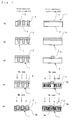
- Figure 2 (a) is a diagram which shows the quartz quasi-phase matching element 1.
- a positive type resist layer 5 having a thickness sufficient to cover the protruding parts 2 is formed on the surface of this quasi-phase matching element 1 ( Figure 2 (b)).
- the resist is exposed by lithography so that the central portion in the cross-section along line B-B of the quasi-phase matching element 1 is left "as is”, and the resist is developed, so that a portion in which the resist 5 remains is formed in the central part ( Figure 2 (c)).
- the resist layer 5 is removed, and He ions with a different energy from those used in the step shown in Figure 2 (d) are implanted. Specifically, the energy of the He ions implanted in this case is increased, so that the ions do not stop in portions that are close to the surface of the substrate, but instead accumulate at a certain depth. Consequently, a low-refractive-index region 6b is newly formed in a position located at a specified depth ( Figure 2 (e)).
- the high-refractive-index region 7 is formed so that this region passes through the plurality of portions with inverted crystal axes (polarization inversion regions) 4. Accordingly, if light is caused to pass through this high-refractive-index region 7, the light can be caused to pass through the portions with inverted crystal axes (polarization inversion regions) 4, and can be subjected to a wavelength conversion, in a state in which the light is confined into the high-refractive-index region 7. Consequently, a state can be produced in which the energy of the light is high inside the wavelength conversion element, so that a high wavelength conversion efficiency can be obtained.
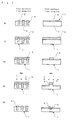
- FIG. 3 shows sectional views along line A-A and sectional views along line B-B in Figure 1 (a).
- Figure 3 (a) is a diagram showing the quartz quasi-phase matching element 1.
- a negative type resist layer 5 with a thickness sufficient to cover the protruding parts 2 is formed on the surface of this quasi-phase matching element 1 ( Figure 3 (b)).
- the central portion of the quasi-phase matching element 1 in the sectional view along line B-B is exposed by lithography over a specified width in the left-right direction in Figure 1, and the resist is developed, so that the resist is removed with the exposed portion left "as is" ( Figure 3 (c)).
- the protruding part 8 is formed so as to pass through the plurality of portions with inverted crystal axes (polarization inversion regions) 4, and the ridge type waveguide 9 is formed in the lower part of this protruding part. Accordingly, light can be caused to pass through the portions with inverted crystal axes (polarization inversion regions) 4, and thus subjected to a wavelength conversion, in a state in which the light is confined inside the ridge type waveguide 9, by causing this light to pass through the ridge type waveguide 9. Consequently, a state can be produced in which the energy of the light is high inside the wavelength conversion element, so that a high wavelength conversion efficiency can be obtained.
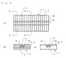
- Figure 4 (a) is a plan view
- Figure 4 (b) is a sectional view along line A-A in Figure 4 (a)
- Figure 4 (c) is a sectional view along line B-B in Figure 4 (a).
- the wavelength conversion element shown in Figure 4 is formed by forming grooves by means of dicing in the quartz quasi-phase matching element 1 shown in Figure 1. Specifically, two grooves 10 are diced in parallel along the light passage direction. Consequently, as is shown in Figures 4 (b) and 4 (c), a protruding part 11 which is positioned between the two grooves 10 is formed on the upper surface in the figures, and a ridge type waveguide 9 is formed inside this protruding part. Accordingly, light can be caused to pass through the portions with inverted crystal axes (polarization inversion regions) 4, and thus subjected to a wavelength conversion, in a state in which the light is confined inside the ridge type waveguide 9, by causing the light to pass through this ridge type waveguide 9. Consequently, a state can be produced in which the intensity of the light is high inside the wavelength conversion element, so that a high wavelength conversion efficiency can be obtained.
- this method since the formation of the ridge type waveguide 9 is accomplished by mechanical working, the process is simple; furthermore, since there is no use of ion implantation, etc., this method is characterized by the fact that there is no alteration of the properties of the portions with inverted crystal axes (polarization inversion regions) 4.
- the low-refractive-index substance that is used to form the ridge type waveguide 9 is air; however, it would also be possible, for example, to cover the upper surface of the waveguide conversion element shown in Figures 3 and 4 with a substance that has a lower refractive index than quartz.
Landscapes
- Physics & Mathematics (AREA)
- Nonlinear Science (AREA)
- General Physics & Mathematics (AREA)
- Optics & Photonics (AREA)
- Optical Modulation, Optical Deflection, Nonlinear Optics, Optical Demodulation, Optical Logic Elements (AREA)
Abstract
Description
→ Li1-xHxNbO3 + (C6H5COOLi)x
Claims (5)
- A wavelength conversion element in which a plurality of polarization inversion regions are formed in a quartz crystal substrate in a periodic manner, and light that is incident from one end of the quartz crystal substrate is subjected to a wavelength conversion by being caused to pass through the plurality of polarization inversion regions, this wavelength conversion element being characterized in that a high-refractive-index region is formed so that this region passes through the plurality of polarization inversion regions in the direction of light transmission.
- The wavelength conversion element according to Claim 1, which is characterized in that the high-refractive-index region is formed by converting the area around this region into a low-refractive-index region by means of ion implantation.
- The wavelength conversion element according to Claim 1, which is characterized in that the high-refractive-index region is formed by a ridge type waveguide.
- The wavelength conversion element according to Claim 3, which is characterized in that the ridge type waveguide is formed by selective reactive ion etching.
- The wavelength conversion element according to Claim 3, which is characterized in that the ridge type waveguide is formed by mechanical working.
Applications Claiming Priority (3)
| Application Number | Priority Date | Filing Date | Title |
|---|---|---|---|
| JP2002276000A JP2004109915A (en) | 2002-09-20 | 2002-09-20 | Wavelength conversion element |
| JP2002276000 | 2002-09-20 | ||
| PCT/JP2003/011881 WO2004027512A1 (en) | 2002-09-20 | 2003-09-18 | Wavelength conversion element |
Publications (2)
| Publication Number | Publication Date |
|---|---|
| EP1542070A1 true EP1542070A1 (en) | 2005-06-15 |
| EP1542070A4 EP1542070A4 (en) | 2008-09-03 |
Family
ID=32025050
Family Applications (1)
| Application Number | Title | Priority Date | Filing Date |
|---|---|---|---|
| EP03797651A Withdrawn EP1542070A4 (en) | 2002-09-20 | 2003-09-18 | WAVE LENGTH CONVERSION ELEMENT |
Country Status (4)
| Country | Link |
|---|---|
| US (1) | US7177070B2 (en) |
| EP (1) | EP1542070A4 (en) |
| JP (1) | JP2004109915A (en) |
| WO (1) | WO2004027512A1 (en) |
Families Citing this family (4)
| Publication number | Priority date | Publication date | Assignee | Title |
|---|---|---|---|---|
| JP2004109914A (en) * | 2002-09-20 | 2004-04-08 | Nikon Corp | Method for manufacturing quasi-phase matched crystal and quasi-phase matched crystal |
| JP4209162B2 (en) * | 2002-09-20 | 2009-01-14 | 株式会社ニコン | PRESSING DEVICE AND METHOD FOR PRODUCING CRYSTAL WITH PHASE TRANSITION TYPE |
| JP2006017925A (en) * | 2004-06-30 | 2006-01-19 | Kyocera Kinseki Corp | Optical waveguide and method for manufacturing the same |
| WO2008133178A1 (en) * | 2007-04-18 | 2008-11-06 | Nikon Corporation | Wavelength conversion element, wavelength conversion method, phase matching method, and light source device |
Family Cites Families (6)
| Publication number | Priority date | Publication date | Assignee | Title |
|---|---|---|---|---|
| JPH03237437A (en) | 1990-02-15 | 1991-10-23 | Asahi Glass Co Ltd | Polarization domain inversion distribution type optical waveguide element |
| JP3364268B2 (en) | 1992-10-21 | 2003-01-08 | パイオニア株式会社 | Method of forming domain-inverted layer |
| US5581642A (en) * | 1994-09-09 | 1996-12-03 | Deacon Research | Optical frequency channel selection filter with electronically-controlled grating structures |
| JPH11212128A (en) * | 1998-01-23 | 1999-08-06 | Mitsubishi Materials Corp | Wavelength conversion element, method of manufacturing the same, and solid-state laser device using the same |
| US6631231B2 (en) | 2000-03-21 | 2003-10-07 | Matsushita Electric Industrial Co., Ltd. | Optical waveguide elements, optical wavelength conversion elements, and process for producing optical waveguide elements |
| JP2002122898A (en) * | 2000-06-29 | 2002-04-26 | Nikon Corp | Coherent light source, semiconductor exposure device, laser treatment device, laser interferometer device, laser microscope device |
-
2002
- 2002-09-20 JP JP2002276000A patent/JP2004109915A/en active Pending
-
2003
- 2003-09-18 EP EP03797651A patent/EP1542070A4/en not_active Withdrawn
- 2003-09-18 WO PCT/JP2003/011881 patent/WO2004027512A1/en not_active Ceased
- 2003-09-18 US US10/522,698 patent/US7177070B2/en not_active Expired - Lifetime
Also Published As
| Publication number | Publication date |
|---|---|
| EP1542070A4 (en) | 2008-09-03 |
| JP2004109915A (en) | 2004-04-08 |
| US20050174629A1 (en) | 2005-08-11 |
| WO2004027512A1 (en) | 2004-04-01 |
| US7177070B2 (en) | 2007-02-13 |
Similar Documents
| Publication | Publication Date | Title |
|---|---|---|
| Hu et al. | Lithium niobate-on-insulator (LNOI): status and perspectives | |
| Thomas et al. | Laser direct writing: Enabling monolithic and hybrid integrated solutions on the lithium niobate platform | |
| US6952307B2 (en) | Electric field poling of ferroelectric materials | |
| US7170671B2 (en) | High efficiency wavelength converters | |
| WO2001006313A1 (en) | Periodic thermal poling of waveguides for quasi phase matching | |
| US7177070B2 (en) | Wavelength conversion element | |
| US20180031949A1 (en) | Heterogeneous waveguides and methods of manufacture | |
| EP1114343B1 (en) | Fabrication of optical waveguides | |
| Wang et al. | Second-harmonic generation in nanophotonic PPLN waveguides with ultrahigh efficiencies | |
| Hu et al. | Towards nonlinear photonic wires in lithium niobate | |
| Zhao et al. | Lithium niobate ridge waveguides fabricated by ion implantation followed by ion beam etching | |
| JPH10142645A (en) | Wavelength converter | |
| Baghban et al. | Low-loss ridge waveguides in thin film lithium niobate-on-insulator (LNOI) fabricated by reactive ion etching | |
| WO2005052682A1 (en) | Fabrication of optical waveguides in periodically poled lithium niobate | |
| EP1542069A1 (en) | Method of producing quasi phase-matching crystal and quasi phase-matching crystal | |
| KR100878978B1 (en) | Method for manufacturing PPIEL waveguide device using laser | |
| Samarelli | Micro ring resonators in silicon-on-insulator | |
| Krasnokutska | Photonic circuits engineering in lithium niobate on insulator | |
| JP3842427B2 (en) | Optical waveguide component and manufacturing method thereof | |
| Chen et al. | Photonic structures based on thin films produced by ion beams | |
| Webjorn | Quasi-phase-matching waveguides for optical second harmonic generation. | |
| Martinez-Jimenez | Laser processing of amorphous silicon for photonic applications | |
| Kajal | Design and implementation of novel nonlinear processes in bulk and waveguide periodic structures | |
| Bremer | Periodically Poled RidgeWaveguides in LiNbO3 | |
| Fujimura et al. | LiNbO3 waveguide SHG devices based on a ferroelectric domain‐inverted grating induced by SiO2cladding |
Legal Events
| Date | Code | Title | Description |
|---|---|---|---|
| PUAI | Public reference made under article 153(3) epc to a published international application that has entered the european phase |
Free format text: ORIGINAL CODE: 0009012 |
|
| 17P | Request for examination filed |
Effective date: 20050218 |
|
| AK | Designated contracting states |
Kind code of ref document: A1 Designated state(s): AT BE BG CH CY CZ DE DK EE ES FI FR GB GR HU IE IT LI LU MC NL PT RO SE SI SK TR |
|
| AX | Request for extension of the european patent |
Extension state: AL LT LV MK |
|
| DAX | Request for extension of the european patent (deleted) | ||
| RBV | Designated contracting states (corrected) |
Designated state(s): DE FR GB |
|
| A4 | Supplementary search report drawn up and despatched |
Effective date: 20080806 |
|
| 17Q | First examination report despatched |
Effective date: 20081106 |
|
| STAA | Information on the status of an ep patent application or granted ep patent |
Free format text: STATUS: THE APPLICATION IS DEEMED TO BE WITHDRAWN |
|
| 18D | Application deemed to be withdrawn |
Effective date: 20090317 |