EP1542047B1 - Fokusierende Vorrichtung für optische Fasern und Antennen, die faseroptische Gitter enthalten - Google Patents
Fokusierende Vorrichtung für optische Fasern und Antennen, die faseroptische Gitter enthalten Download PDFInfo
- Publication number
- EP1542047B1 EP1542047B1 EP04106431A EP04106431A EP1542047B1 EP 1542047 B1 EP1542047 B1 EP 1542047B1 EP 04106431 A EP04106431 A EP 04106431A EP 04106431 A EP04106431 A EP 04106431A EP 1542047 B1 EP1542047 B1 EP 1542047B1
- Authority
- EP
- European Patent Office
- Prior art keywords
- semi
- plane
- reflecting mirror
- optical
- dielectric
- Prior art date
- Legal status (The legal status is an assumption and is not a legal conclusion. Google has not performed a legal analysis and makes no representation as to the accuracy of the status listed.)
- Expired - Lifetime
Links
Images


Classifications
-
- H—ELECTRICITY
- H01—ELECTRIC ELEMENTS
- H01Q—ANTENNAS, i.e. RADIO AERIALS
- H01Q3/00—Arrangements for changing or varying the orientation or the shape of the directional pattern of the waves radiated from an antenna or antenna system
- H01Q3/26—Arrangements for changing or varying the orientation or the shape of the directional pattern of the waves radiated from an antenna or antenna system varying the relative phase or relative amplitude of energisation between two or more active radiating elements; varying the distribution of energy across a radiating aperture
- H01Q3/2676—Optically controlled phased array
-
- G—PHYSICS
- G02—OPTICS
- G02B—OPTICAL ELEMENTS, SYSTEMS OR APPARATUS
- G02B6/00—Light guides; Structural details of arrangements comprising light guides and other optical elements, e.g. couplings
- G02B6/24—Coupling light guides
- G02B6/26—Optical coupling means
- G02B6/262—Optical details of coupling light into, or out of, or between fibre ends, e.g. special fibre end shapes or associated optical elements
-
- G—PHYSICS
- G02—OPTICS
- G02B—OPTICAL ELEMENTS, SYSTEMS OR APPARATUS
- G02B6/00—Light guides; Structural details of arrangements comprising light guides and other optical elements, e.g. couplings
- G02B6/24—Coupling light guides
- G02B6/42—Coupling light guides with opto-electronic elements
- G02B6/4201—Packages, e.g. shape, construction, internal or external details
- G02B6/4204—Packages, e.g. shape, construction, internal or external details the coupling comprising intermediate optical elements, e.g. lenses, holograms
- G02B6/4206—Optical features
Definitions
- the present invention relates to a focusing device for optical fibers. It applies in particular in the field of opto-microwave links. More particularly, it applies in microwave modules comprising optical components.
- the invention also relates to an optical fiber network antenna equipped with the aforementioned focusing device.
- Optical components can be advantageously used in radar applications and more generally in applications using microwave techniques.
- information for controlling and controlling microwave signals can be conveyed by optical waves. This may be the case, for example, in electronic scanning antennas with regard to the phase shift diode control circuits.
- optical components can be integrated in microwave switches. Among the advantages of optical techniques are high bandwidth and very low sensitivity to microwave interference.
- a significant problem in the techniques coupling the optical waves and the microwave waves is the opto-microwave junction, that is to say the passage of a signal from the optical domain to the microwave domain or vice versa.
- the transmitted power can be very degraded at the passage of such a junction.
- the optical fibers can be used in microwave modules to bring for example control signals.
- the optical signal at the output of the fiber then meets an opto-microwave receiver.
- the output beam of the fiber must be relatively narrow, so high directivity, so as to concentrate the energy on the opto-microwave interface. If the optical beam at the output of a fiber is too large a good part of the transmitted energy is lost.
- a document US 3,704,996 discloses an optical coupling device for transmitting a light beam between two optical fibers.
- An object of the invention is in particular to allow focusing of the optical beam at the output of the fiber.
- the invention relates to a focusing device for optical fiber as described by claims 1 to 6.
- the invention also relates to an antenna comprising a reflective plane and a substantially parallel semi-reflective plane forming a focusing device as previously described.
- the figure 1 shows schematically, in a sectional view an optical fiber 1 surrounded by a sheath 2.
- This optical fiber is for example integrated in a microwave module. It conveys for example an optical signal modulated by a microwave signal.
- the fiber is for example coupled to its output to an optoelectronic component not shown. This optoelectronic component then ensures the conversion between the optical signal and the microwave signal. It thus restores a microwave signal subsequently processed by conventional microwave circuits, in a radar for example.
- the coupling at the output of optical fiber with other components, in particular optoelectronic components, is via its optical beam 3.
- FIG. figure 1 in the absence of a device focusing the optical beam at the output of the fiber 1 is wide, it is weakly directional. Such a beam is not optimum from the point of view of energy efficiency. Indeed, a large part of the energy is not transmitted to the receiver component.
- the figure 2 shows an ideal case of focused beam 3 'where all the energy conveyed by the beam 3' can be transmitted to the receiving component.
- the beam is highly directive.
- solutions for focusing an optical beam It is of course possible to use a lens for this purpose. Nevertheless, such a solution has several disadvantages. In particular, it entails a complexity of realization and development due in particular to the precise positioning and adjustment required because of the dimensions of the optical fiber. In case of application in a constraining environment, in cases for example subjected to vibrations, these constraints become even more difficult to hold. This results in additional cost.
- the figure 3 presents an exemplary embodiment of a focusing device according to the invention equipping an optical fiber.
- the device comprises a partially conductive plane 31 parallel to a reflective plane 42 on which opens the optical fiber 1 forming a radiating aperture.
- the reflective plane is for example the transverse plane of the sheath at the output of the optical fiber 1, this plane being made reflective.
- the device according to the invention is placed at the output of the fiber 1. It therefore comprises a plane semi-reflecting mirror 31 disposed at a distance d from the output of the optical fiber 1.
- a dielectric 32 is interposed between the mirror 31 and the fiber.
- the dielectric 32 is for example a silica log, having in particular the same diameter as the sheath and extending it.
- the mirror 32 is for example a layer composed of a mixture of titanium oxide (TiO 2 ) and silicon oxide or silica (SiO 2 ) deposited for example on the silica log 32.
- the dielectric 32 has the same dielectric constant ⁇ as the core of the optical fiber 1 to avoid particular problems of mismatching the wave output of the fiber.
- the relative dielectric constant ⁇ r is for example of the order of 1.5. However, other dielectric constants than that of the optical fiber 1 can be admitted.
- the dielectric medium may for example be ambient air.
- the thickness of the semi-reflecting mirror 31 is, for example, of the order of 0.25 ⁇ , where ⁇ is the length of the optical wave at the output of the fiber.
- ⁇ is the length of the optical wave at the output of the fiber.
- the figure 4 explains the operation of a device according to the invention.
- the optical fiber 1 is represented by its axis 41.
- the semi-reflecting mirror 31 is placed at the distance d from the reflector plane 42.
- the reflective plane is for example the transverse plane of the sheath 2 at the output of optical fiber .
- This plan is metallic. If the sheath is not made of metallic material, this transverse plane 42 can then be covered with a metal layer.
- the device according to the invention associated with the optical fiber 1 thus has a radiating opening or initial source S 0 , the output of the fiber, in the center of a reflector plane 42.
- the plane of the semi-reflecting mirror 31 parallel to the previous one introduces , in addition to the initial radiation R 0 , multiple reflections R 1 , R 2 , R 3 ... at decreasing amplitudes. These multiple reflections are parallel to the initial radiation R 0 .
- the figure 4 illustrates this initial radiation for an angle ⁇ around the axis of the optical fiber 1.
- the reflections form a series of images and virtual sources S 1 , S 2 ... behind the initial source S 0 .
- the space between two sources is twice the distance d between the planes 42, 32.
- the reflection coefficient of the semi-reflecting mirror 31 is equal to ⁇ .e j ⁇ , ⁇ being the phase shift applied by the mirror to the optical wave.
- the coefficient of Power reflection is therefore ⁇ 2 and according to the conservation of energy (1- ⁇ 2 ) is the power transmission coefficient.
- the module M 0 of the initial radiation R 0 after passing through the semi-reflecting mirror 31 is f ⁇ ⁇ E 0 ⁇ 1 - ⁇ 2
- E 0 is the amplitude of the wave at the optical fiber output and in the axis 41 of the fiber
- f ( ⁇ ) E 0 is then the amplitude of the wave in the direction that makes an angle ⁇ with this axis 41.
- E 0 is the intensity of the optical signal at the output of the source, that is to say at the output of the optical fiber
- f ( ⁇ ) is the source diagram.
- f ( ⁇ ) E 0 is illustrated by the beam 3 of the optical fiber in figure 1 .
- the phase angle ⁇ n is the composition of the phase delays due to the multiple reflections between the two planes 42, 31 and also to the propagation delay of the transmitted line. An additional phase appears when a radiation passes through the semi-reflecting mirror 32. However, since this is the case for all the radiation R 1 , R 2 , R 3 ..., there is no need to take into account.
- phase change term appears when crossing the dielectric 32. This term returns to each radiation, it vanishes when the phase difference is expressed.
- the term - ⁇ is due to the phase inversion during the reflection on the reflective plane 42.
- the term + ⁇ appears during the reflection on the semi-reflecting mirror 31.
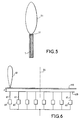
- the semi-reflecting mirror 31 is also chosen so that the modulus p of its reflection coefficient is the largest possible since the directivity increases with this module ⁇ . It is then possible to obtain a radiation diagram 51 at the output of the device according to the invention as illustrated by FIG. figure 5 and getting closer to the ideal case of the figure 2 .
- the semi-reflecting mirror is for example made by a TiO 2 -SiO 2 mixture layer whose modulus of the reflection coefficient ⁇ can be controlled.
- the reflection coefficient can be determined by the proportion of titanium oxide (SiO 2 ) in the TiO 2 -SiO 2 mixture. The directivity of the output beam 51 can thus be controlled by varying this proportion.
- the composite can also be an oxide of the type: Ti x ⁇ Yes 1 - x ⁇ O 2 or 0 ⁇ x ⁇ 1 where 0 ⁇ x ⁇ 1
- the reflection coefficient p can for example play on the molar fraction x.
- the figure 6 presents an exemplary embodiment of an antenna according to the invention.
- This antenna works for example in the infrared field.
- This antenna comprises a network of N optical fibers 61.
- figure 6 presents a network in one dimension, the network can of course be two-dimensional.
- Each optical fiber 61 opens onto a reflective plane 420, for example a metal plane.
- a semi-reflective plane 310 is placed parallel to the distance d from the reflector plane 420 facing the outlet of the optical fibers.
- the two planes 310, 420 are separated by a distance d. This distance as well as the parameters of the reflection coefficient of the semi-reflecting mirror are defined so as to obtain the desired directivity for the output beams 62 as indicated previously in the case of a single fiber.
- the optical waves are controlled by control devices 63.
- the Figures 7a and 7b illustrate the antenna pattern of the figure 6 .
- the figure 7a presents the source gain g ( ⁇ ) and the grating factor F ( ⁇ ) 71 taken independently.
- the figure 7b illustrates the product g ( ⁇ ) x F ( ⁇ ). This figure shows that the antenna beam obtained is very directional.
Landscapes
- Physics & Mathematics (AREA)
- General Physics & Mathematics (AREA)
- Optics & Photonics (AREA)
- Aerials With Secondary Devices (AREA)
- Light Guides In General And Applications Therefor (AREA)
- Optical Integrated Circuits (AREA)
- Optical Couplings Of Light Guides (AREA)
- Manufacture, Treatment Of Glass Fibers (AREA)
Claims (9)
- Fokussierungsvorrichtung für Lichtleitfaser, dadurch gekennzeichnet, dass sie einen halb reflektierenden ebenen Spiegel (31) und eine Reflexionsebene (42), auf der die Lichtleitfaser, die eine strahlende Öffnung (S) bildet, mündet, aufweist, wobei die zwei Ebenen (31, 42) von einer Entfernung d durch ein Dielektrikum (32) getrennt sind, wobei die Ebene des halb reflektierenden Spiegels im Wesentlichen zu der Reflexionsebene parallel ist, wobei der halb reflektierende Spiegel von Strahlungen (R1,R2, R3, ..., Rn), die zu der Strahlung R0 der strahlenden Öffnung parallel sind, durchquert werden kann, mit abnehmenden Amplituden, wobei die Richtfähigkeit des Strahlenbündels von dem Reflexionskoeffizienten ρ des halb reflektierenden Spiegels abhängt, wobei der halb reflektierende Spiegel (31) eingerichtet ist, um die Gleichung der Verstärkung S des Strahlungsdiagramms am Ausgang der Vorrichtung:


- Vorrichtung nach Anspruch 1, dadurch gekennzeichnet, dass die reflektierende Ebene (42) die Querebene der Hülle (2) der Lichtleitfaser auf dem Niveau ihres Ausgangs ist.
- Vorrichtung nach Anspruch 2, dadurch gekennzeichnet, dass ein Dielektrikum (32) die zwei Ebenen (31, 42) trennt, wobei dieses Dielektrikum die Form einer Stange hat, die die Hülle (2) der Lichtleitfaser verlängert.
- Vorrichtung nach Anspruch 2, dadurch gekennzeichnet, dass der halb reflektierende Spiegel die Form einer auf dem Dielektrikum aufgebrachten Schicht hat.
- Vorrichtung nach einem der vorhergehenden Ansprüche, dadurch gekennzeichnet, dass der halb reflektierende Spiegel aus einem Gemisch aus Titanoxid (TiO2) und Siliciumoxid (SiO2) besteht.
- Vorrichtung nach einem der Ansprüche 1 bis 4, dadurch gekennzeichnet, dass der reflektierende Spiegel aus einem Oxid des folgenden Typs besteht:
TixSi1-xO2, 0 < x < 1.
- Anntenne, die eine große Richtfähigkeit besitzt, dadurch gekennzeichnet, dass sie eine reflektierende Ebene (420) und eine halb reflektierende Ebene (320), die im Wesentlichen parallel sind, aufweist, die eine Fokussierungsvorrichtung nach einem der Ansprüche 1 bis 9 bilden, und mehrere Lichtleitfasern, die in der reflektierenden Ebene gegenüber der halb reflektierenden Ebene münden.
- Antenne nach Anspruch 7, dadurch gekennzeichnet, dass die mehreren Lichtleitfasern ein lineares Netz bilden.
- Antenne nach Anspruch 7, dadurch gekennzeichnet, dass die mehreren Lichtleitfasern ein ebenes Netz bilden.
Applications Claiming Priority (2)
| Application Number | Priority Date | Filing Date | Title |
|---|---|---|---|
| FR0314594A FR2863717B1 (fr) | 2003-12-12 | 2003-12-12 | Dispositif focalisant pour fibres optiques et antenne a reseau de fibres optiques |
| FR0314594 | 2003-12-12 |
Publications (2)
| Publication Number | Publication Date |
|---|---|
| EP1542047A1 EP1542047A1 (de) | 2005-06-15 |
| EP1542047B1 true EP1542047B1 (de) | 2009-04-01 |
Family
ID=34508654
Family Applications (1)
| Application Number | Title | Priority Date | Filing Date |
|---|---|---|---|
| EP04106431A Expired - Lifetime EP1542047B1 (de) | 2003-12-12 | 2004-12-09 | Fokusierende Vorrichtung für optische Fasern und Antennen, die faseroptische Gitter enthalten |
Country Status (4)
| Country | Link |
|---|---|
| EP (1) | EP1542047B1 (de) |
| AT (1) | ATE427512T1 (de) |
| DE (1) | DE602004020312D1 (de) |
| FR (1) | FR2863717B1 (de) |
Family Cites Families (3)
| Publication number | Priority date | Publication date | Assignee | Title |
|---|---|---|---|---|
| US3704996A (en) * | 1969-10-23 | 1972-12-05 | Licentia Gmbh | Optical coupling arrangement |
| KR100553877B1 (ko) * | 1999-04-29 | 2006-02-24 | 삼성전자주식회사 | 광소자모듈 |
| WO2003090384A1 (en) * | 2002-04-19 | 2003-10-30 | Imego Ab | An arrangement for transmitting and/or receiving electromagnetic signals |
-
2003
- 2003-12-12 FR FR0314594A patent/FR2863717B1/fr not_active Expired - Fee Related
-
2004
- 2004-12-09 EP EP04106431A patent/EP1542047B1/de not_active Expired - Lifetime
- 2004-12-09 DE DE602004020312T patent/DE602004020312D1/de not_active Expired - Lifetime
- 2004-12-09 AT AT04106431T patent/ATE427512T1/de not_active IP Right Cessation
Also Published As
| Publication number | Publication date |
|---|---|
| EP1542047A1 (de) | 2005-06-15 |
| FR2863717B1 (fr) | 2006-02-03 |
| DE602004020312D1 (de) | 2009-05-14 |
| FR2863717A1 (fr) | 2005-06-17 |
| ATE427512T1 (de) | 2009-04-15 |
Similar Documents
| Publication | Publication Date | Title |
|---|---|---|
| FR2477286A1 (fr) | Dispositif a fibre optique et emetteur de lumiere utilisant le dispositif | |
| EP3665744B1 (de) | Vorrichtung zur optischen aufnahme eines von einer phasengesteuerten antennenanordnung kommenden signals und zugehöriges antennensystem | |
| FR2833768A1 (fr) | Laser a resonnateur externe accordable en longueur d'onde utilisant un deflecteur optique | |
| FR2908931A1 (fr) | Antenne et emetteur/recepteur terahertz integres,et procede pour leur fabrication. | |
| FR2570839A1 (fr) | Dispositif de couplage entre des guides d'onde, monolithiquement integre avec ceux-ci sur un substrat semiconducteur | |
| EP2143181B1 (de) | Kompakte laserquelle mit verringerter spektraler breite | |
| Hashemi | A review of silicon photonics LiDAR | |
| US10082624B2 (en) | System for coupling radiation into a waveguide | |
| EP0947033B1 (de) | Sende- und empfangsvorrichtung für mikrowellen | |
| FR2614136A1 (fr) | Dispositif de commande optique d'une antenne a balayage | |
| Zhang et al. | A fully solid-state beam scanner for FMCW LiDAR application | |
| FR2743234A1 (fr) | Demultiplexeur de longueurs d'onde | |
| EP1542047B1 (de) | Fokusierende Vorrichtung für optische Fasern und Antennen, die faseroptische Gitter enthalten | |
| US5530778A (en) | Direction finding apparatus using tunable fiber optic delay line | |
| US12113144B2 (en) | Arrangement for an antenna for generating or receiving terahertz radiation, antenna, terahertz system, and method for producing an arrangement for an antenna | |
| EP0559551A1 (de) | Optischer Koppler mit hoher Übersprechdämpfung | |
| FR2871297A1 (fr) | Dispositif de formation de faisceaux a la reception pour une antenne a elements rayonnants | |
| EP2104871A1 (de) | Vorrichtung zur abtastung mehrerer teile eines lichtstrahls | |
| EP4010932B1 (de) | Planare optoelektronische vorrichtung zur erzeugung eines mikrowellensignals | |
| FR2787588A1 (fr) | Systeme lidar et application a un systeme radar | |
| Goldsmith | Diffraction loss in dielectric-filled Fabry-Perot interferometers | |
| FR2688074A1 (fr) | Dispositif de deflexion angulaire acousto-optique, et analyseur de spectre utilisant un tel dispositif. | |
| JP4766871B2 (ja) | 光ファイバ用集束装置及び光ファイバ・アレー・アンテナ | |
| JP2025037175A (ja) | 光通信用受光素子及び光通信デバイス | |
| CA3239765A1 (fr) | Emetteur optoelectronique a antenne reseau a commande de phase comportant des antennes optiques adaptees a emettre un rayonnement lumineux selon un profil d'emission et une direction predefinis |
Legal Events
| Date | Code | Title | Description |
|---|---|---|---|
| PUAI | Public reference made under article 153(3) epc to a published international application that has entered the european phase |
Free format text: ORIGINAL CODE: 0009012 |
|
| AK | Designated contracting states |
Kind code of ref document: A1 Designated state(s): AT BE BG CH CY CZ DE DK EE ES FI FR GB GR HU IE IS IT LI LT LU MC NL PL PT RO SE SI SK TR |
|
| AX | Request for extension of the european patent |
Extension state: AL BA HR LV MK YU |
|
| AKX | Designation fees paid | ||
| 17P | Request for examination filed |
Effective date: 20051207 |
|
| RBV | Designated contracting states (corrected) |
Designated state(s): AT BE BG CH CY CZ DE DK EE ES FI FR GB GR HU IE IS IT LI LT LU MC NL PL PT RO SE SI SK TR |
|
| REG | Reference to a national code |
Ref country code: DE Ref legal event code: 8566 |
|
| GRAP | Despatch of communication of intention to grant a patent |
Free format text: ORIGINAL CODE: EPIDOSNIGR1 |
|
| GRAS | Grant fee paid |
Free format text: ORIGINAL CODE: EPIDOSNIGR3 |
|
| GRAA | (expected) grant |
Free format text: ORIGINAL CODE: 0009210 |
|
| AK | Designated contracting states |
Kind code of ref document: B1 Designated state(s): AT BE BG CH CY CZ DE DK EE ES FI FR GB GR HU IE IS IT LI LT LU MC NL PL PT RO SE SI SK TR |
|
| REG | Reference to a national code |
Ref country code: GB Ref legal event code: FG4D Free format text: NOT ENGLISH |
|
| REG | Reference to a national code |
Ref country code: CH Ref legal event code: EP |
|
| REG | Reference to a national code |
Ref country code: IE Ref legal event code: FG4D Free format text: LANGUAGE OF EP DOCUMENT: FRENCH |
|
| REF | Corresponds to: |
Ref document number: 602004020312 Country of ref document: DE Date of ref document: 20090514 Kind code of ref document: P |
|
| REG | Reference to a national code |
Ref country code: SE Ref legal event code: TRGR |
|
| PG25 | Lapsed in a contracting state [announced via postgrant information from national office to epo] |
Ref country code: SI Free format text: LAPSE BECAUSE OF FAILURE TO SUBMIT A TRANSLATION OF THE DESCRIPTION OR TO PAY THE FEE WITHIN THE PRESCRIBED TIME-LIMIT Effective date: 20090401 |
|
| NLV1 | Nl: lapsed or annulled due to failure to fulfill the requirements of art. 29p and 29m of the patents act | ||
| REG | Reference to a national code |
Ref country code: IE Ref legal event code: FD4D |
|
| PG25 | Lapsed in a contracting state [announced via postgrant information from national office to epo] |
Ref country code: PT Free format text: LAPSE BECAUSE OF FAILURE TO SUBMIT A TRANSLATION OF THE DESCRIPTION OR TO PAY THE FEE WITHIN THE PRESCRIBED TIME-LIMIT Effective date: 20090902 Ref country code: ES Free format text: LAPSE BECAUSE OF FAILURE TO SUBMIT A TRANSLATION OF THE DESCRIPTION OR TO PAY THE FEE WITHIN THE PRESCRIBED TIME-LIMIT Effective date: 20090712 Ref country code: EE Free format text: LAPSE BECAUSE OF FAILURE TO SUBMIT A TRANSLATION OF THE DESCRIPTION OR TO PAY THE FEE WITHIN THE PRESCRIBED TIME-LIMIT Effective date: 20090401 Ref country code: FI Free format text: LAPSE BECAUSE OF FAILURE TO SUBMIT A TRANSLATION OF THE DESCRIPTION OR TO PAY THE FEE WITHIN THE PRESCRIBED TIME-LIMIT Effective date: 20090401 Ref country code: AT Free format text: LAPSE BECAUSE OF FAILURE TO SUBMIT A TRANSLATION OF THE DESCRIPTION OR TO PAY THE FEE WITHIN THE PRESCRIBED TIME-LIMIT Effective date: 20090401 Ref country code: LT Free format text: LAPSE BECAUSE OF FAILURE TO SUBMIT A TRANSLATION OF THE DESCRIPTION OR TO PAY THE FEE WITHIN THE PRESCRIBED TIME-LIMIT Effective date: 20090401 |
|
| PG25 | Lapsed in a contracting state [announced via postgrant information from national office to epo] |
Ref country code: IS Free format text: LAPSE BECAUSE OF FAILURE TO SUBMIT A TRANSLATION OF THE DESCRIPTION OR TO PAY THE FEE WITHIN THE PRESCRIBED TIME-LIMIT Effective date: 20090801 Ref country code: PL Free format text: LAPSE BECAUSE OF FAILURE TO SUBMIT A TRANSLATION OF THE DESCRIPTION OR TO PAY THE FEE WITHIN THE PRESCRIBED TIME-LIMIT Effective date: 20090401 Ref country code: NL Free format text: LAPSE BECAUSE OF FAILURE TO SUBMIT A TRANSLATION OF THE DESCRIPTION OR TO PAY THE FEE WITHIN THE PRESCRIBED TIME-LIMIT Effective date: 20090401 |
|
| PG25 | Lapsed in a contracting state [announced via postgrant information from national office to epo] |
Ref country code: RO Free format text: LAPSE BECAUSE OF FAILURE TO SUBMIT A TRANSLATION OF THE DESCRIPTION OR TO PAY THE FEE WITHIN THE PRESCRIBED TIME-LIMIT Effective date: 20090401 Ref country code: DK Free format text: LAPSE BECAUSE OF FAILURE TO SUBMIT A TRANSLATION OF THE DESCRIPTION OR TO PAY THE FEE WITHIN THE PRESCRIBED TIME-LIMIT Effective date: 20090401 Ref country code: IE Free format text: LAPSE BECAUSE OF FAILURE TO SUBMIT A TRANSLATION OF THE DESCRIPTION OR TO PAY THE FEE WITHIN THE PRESCRIBED TIME-LIMIT Effective date: 20090401 Ref country code: CZ Free format text: LAPSE BECAUSE OF FAILURE TO SUBMIT A TRANSLATION OF THE DESCRIPTION OR TO PAY THE FEE WITHIN THE PRESCRIBED TIME-LIMIT Effective date: 20090401 |
|
| PLBE | No opposition filed within time limit |
Free format text: ORIGINAL CODE: 0009261 |
|
| STAA | Information on the status of an ep patent application or granted ep patent |
Free format text: STATUS: NO OPPOSITION FILED WITHIN TIME LIMIT |
|
| PG25 | Lapsed in a contracting state [announced via postgrant information from national office to epo] |
Ref country code: SK Free format text: LAPSE BECAUSE OF FAILURE TO SUBMIT A TRANSLATION OF THE DESCRIPTION OR TO PAY THE FEE WITHIN THE PRESCRIBED TIME-LIMIT Effective date: 20090401 |
|
| 26N | No opposition filed |
Effective date: 20100105 |
|
| PG25 | Lapsed in a contracting state [announced via postgrant information from national office to epo] |
Ref country code: BG Free format text: LAPSE BECAUSE OF FAILURE TO SUBMIT A TRANSLATION OF THE DESCRIPTION OR TO PAY THE FEE WITHIN THE PRESCRIBED TIME-LIMIT Effective date: 20090701 |
|
| BERE | Be: lapsed |
Owner name: THALES Effective date: 20091231 |
|
| PG25 | Lapsed in a contracting state [announced via postgrant information from national office to epo] |
Ref country code: MC Free format text: LAPSE BECAUSE OF NON-PAYMENT OF DUE FEES Effective date: 20100701 |
|
| REG | Reference to a national code |
Ref country code: CH Ref legal event code: PL |
|
| REG | Reference to a national code |
Ref country code: FR Ref legal event code: ST Effective date: 20100831 |
|
| PG25 | Lapsed in a contracting state [announced via postgrant information from national office to epo] |
Ref country code: BE Free format text: LAPSE BECAUSE OF NON-PAYMENT OF DUE FEES Effective date: 20091231 Ref country code: CH Free format text: LAPSE BECAUSE OF NON-PAYMENT OF DUE FEES Effective date: 20091231 Ref country code: LI Free format text: LAPSE BECAUSE OF NON-PAYMENT OF DUE FEES Effective date: 20091231 Ref country code: GR Free format text: LAPSE BECAUSE OF FAILURE TO SUBMIT A TRANSLATION OF THE DESCRIPTION OR TO PAY THE FEE WITHIN THE PRESCRIBED TIME-LIMIT Effective date: 20090702 Ref country code: FR Free format text: LAPSE BECAUSE OF NON-PAYMENT OF DUE FEES Effective date: 20091231 |
|
| REG | Reference to a national code |
Ref country code: FR Ref legal event code: RN |
|
| REG | Reference to a national code |
Ref country code: FR Ref legal event code: FC |
|
| PGRI | Patent reinstated in contracting state [announced from national office to epo] |
Ref country code: FR Effective date: 20101116 |
|
| PG25 | Lapsed in a contracting state [announced via postgrant information from national office to epo] |
Ref country code: LU Free format text: LAPSE BECAUSE OF NON-PAYMENT OF DUE FEES Effective date: 20091209 |
|
| PG25 | Lapsed in a contracting state [announced via postgrant information from national office to epo] |
Ref country code: HU Free format text: LAPSE BECAUSE OF FAILURE TO SUBMIT A TRANSLATION OF THE DESCRIPTION OR TO PAY THE FEE WITHIN THE PRESCRIBED TIME-LIMIT Effective date: 20091002 |
|
| PG25 | Lapsed in a contracting state [announced via postgrant information from national office to epo] |
Ref country code: TR Free format text: LAPSE BECAUSE OF FAILURE TO SUBMIT A TRANSLATION OF THE DESCRIPTION OR TO PAY THE FEE WITHIN THE PRESCRIBED TIME-LIMIT Effective date: 20090401 |
|
| PG25 | Lapsed in a contracting state [announced via postgrant information from national office to epo] |
Ref country code: CY Free format text: LAPSE BECAUSE OF FAILURE TO SUBMIT A TRANSLATION OF THE DESCRIPTION OR TO PAY THE FEE WITHIN THE PRESCRIBED TIME-LIMIT Effective date: 20090401 |
|
| PGFP | Annual fee paid to national office [announced via postgrant information from national office to epo] |
Ref country code: DE Payment date: 20121205 Year of fee payment: 9 |
|
| PGFP | Annual fee paid to national office [announced via postgrant information from national office to epo] |
Ref country code: SE Payment date: 20121217 Year of fee payment: 9 Ref country code: GB Payment date: 20121205 Year of fee payment: 9 Ref country code: IT Payment date: 20121213 Year of fee payment: 9 |
|
| PGFP | Annual fee paid to national office [announced via postgrant information from national office to epo] |
Ref country code: FR Payment date: 20130107 Year of fee payment: 9 |
|
| REG | Reference to a national code |
Ref country code: DE Ref legal event code: R119 Ref document number: 602004020312 Country of ref document: DE |
|
| REG | Reference to a national code |
Ref country code: SE Ref legal event code: EUG |
|
| GBPC | Gb: european patent ceased through non-payment of renewal fee |
Effective date: 20131209 |
|
| PG25 | Lapsed in a contracting state [announced via postgrant information from national office to epo] |
Ref country code: SE Free format text: LAPSE BECAUSE OF NON-PAYMENT OF DUE FEES Effective date: 20131210 |
|
| REG | Reference to a national code |
Ref country code: DE Ref legal event code: R119 Ref document number: 602004020312 Country of ref document: DE Effective date: 20140701 |
|
| REG | Reference to a national code |
Ref country code: FR Ref legal event code: ST Effective date: 20140829 |
|
| PG25 | Lapsed in a contracting state [announced via postgrant information from national office to epo] |
Ref country code: DE Free format text: LAPSE BECAUSE OF NON-PAYMENT OF DUE FEES Effective date: 20140701 |
|
| PG25 | Lapsed in a contracting state [announced via postgrant information from national office to epo] |
Ref country code: FR Free format text: LAPSE BECAUSE OF NON-PAYMENT OF DUE FEES Effective date: 20131231 Ref country code: GB Free format text: LAPSE BECAUSE OF NON-PAYMENT OF DUE FEES Effective date: 20131209 |
|
| PG25 | Lapsed in a contracting state [announced via postgrant information from national office to epo] |
Ref country code: IT Free format text: LAPSE BECAUSE OF NON-PAYMENT OF DUE FEES Effective date: 20131231 |
|
| PG25 | Lapsed in a contracting state [announced via postgrant information from national office to epo] |
Ref country code: IT Free format text: LAPSE BECAUSE OF NON-PAYMENT OF DUE FEES Effective date: 20131209 |