EP1542006A1 - Impurity measuring method for GE substrates - Google Patents
Impurity measuring method for GE substrates Download PDFInfo
- Publication number
- EP1542006A1 EP1542006A1 EP04447274A EP04447274A EP1542006A1 EP 1542006 A1 EP1542006 A1 EP 1542006A1 EP 04447274 A EP04447274 A EP 04447274A EP 04447274 A EP04447274 A EP 04447274A EP 1542006 A1 EP1542006 A1 EP 1542006A1
- Authority
- EP
- European Patent Office
- Prior art keywords
- drop
- solution
- hcl
- hbr
- substrate
- Prior art date
- Legal status (The legal status is an assumption and is not a legal conclusion. Google has not performed a legal analysis and makes no representation as to the accuracy of the status listed.)
- Granted
Links
- 238000000034 method Methods 0.000 title claims abstract description 49
- 239000000758 substrate Substances 0.000 title claims abstract description 45
- 239000012535 impurity Substances 0.000 title claims abstract description 24
- 238000004458 analytical method Methods 0.000 claims abstract description 20
- 239000000126 substance Substances 0.000 claims abstract description 11
- 150000001875 compounds Chemical class 0.000 claims description 7
- 229910052732 germanium Inorganic materials 0.000 claims description 7
- 238000010438 heat treatment Methods 0.000 claims description 6
- 238000006243 chemical reaction Methods 0.000 claims description 5
- 238000005530 etching Methods 0.000 claims description 5
- 230000001590 oxidative effect Effects 0.000 claims description 5
- GNPVGFCGXDBREM-UHFFFAOYSA-N germanium atom Chemical compound [Ge] GNPVGFCGXDBREM-UHFFFAOYSA-N 0.000 claims description 4
- 229910052751 metal Inorganic materials 0.000 claims description 3
- 239000002184 metal Substances 0.000 claims description 3
- 238000011109 contamination Methods 0.000 abstract description 9
- 239000000243 solution Substances 0.000 description 53
- 235000012431 wafers Nutrition 0.000 description 35
- 239000011159 matrix material Substances 0.000 description 14
- 238000000624 total reflection X-ray fluorescence spectroscopy Methods 0.000 description 11
- 230000002209 hydrophobic effect Effects 0.000 description 6
- 238000011282 treatment Methods 0.000 description 6
- YBMRDBCBODYGJE-UHFFFAOYSA-N germanium oxide Inorganic materials O=[Ge]=O YBMRDBCBODYGJE-UHFFFAOYSA-N 0.000 description 5
- PVADDRMAFCOOPC-UHFFFAOYSA-N oxogermanium Chemical class [Ge]=O PVADDRMAFCOOPC-UHFFFAOYSA-N 0.000 description 5
- 229910052804 chromium Inorganic materials 0.000 description 4
- 239000000356 contaminant Substances 0.000 description 4
- 238000001514 detection method Methods 0.000 description 4
- 238000010790 dilution Methods 0.000 description 4
- 239000012895 dilution Substances 0.000 description 4
- 238000000673 graphite furnace atomic absorption spectrometry Methods 0.000 description 4
- 229910052742 iron Inorganic materials 0.000 description 4
- 238000005259 measurement Methods 0.000 description 4
- 239000000203 mixture Substances 0.000 description 4
- 229910052759 nickel Inorganic materials 0.000 description 4
- 229910052700 potassium Inorganic materials 0.000 description 4
- 229910052791 calcium Inorganic materials 0.000 description 3
- 238000004140 cleaning Methods 0.000 description 3
- 229910052736 halogen Inorganic materials 0.000 description 3
- 150000002367 halogens Chemical class 0.000 description 3
- 150000002823 nitrates Chemical class 0.000 description 3
- 238000002360 preparation method Methods 0.000 description 3
- 229910052706 scandium Inorganic materials 0.000 description 3
- 239000012086 standard solution Substances 0.000 description 3
- 229910001868 water Inorganic materials 0.000 description 3
- 229910052725 zinc Inorganic materials 0.000 description 3
- GRYLNZFGIOXLOG-UHFFFAOYSA-N Nitric acid Chemical compound O[N+]([O-])=O GRYLNZFGIOXLOG-UHFFFAOYSA-N 0.000 description 2
- 239000008346 aqueous phase Substances 0.000 description 2
- 239000007864 aqueous solution Substances 0.000 description 2
- 238000011161 development Methods 0.000 description 2
- 230000001939 inductive effect Effects 0.000 description 2
- 229910017604 nitric acid Inorganic materials 0.000 description 2
- 238000000918 plasma mass spectrometry Methods 0.000 description 2
- 238000004094 preconcentration Methods 0.000 description 2
- 238000012545 processing Methods 0.000 description 2
- 239000012808 vapor phase Substances 0.000 description 2
- XLYOFNOQVPJJNP-UHFFFAOYSA-N water Substances O XLYOFNOQVPJJNP-UHFFFAOYSA-N 0.000 description 2
- 229910006109 GeBr4 Inorganic materials 0.000 description 1
- 229910006113 GeCl4 Inorganic materials 0.000 description 1
- 229910006160 GeF4 Inorganic materials 0.000 description 1
- 229910004014 SiF4 Inorganic materials 0.000 description 1
- XUIMIQQOPSSXEZ-UHFFFAOYSA-N Silicon Chemical compound [Si] XUIMIQQOPSSXEZ-UHFFFAOYSA-N 0.000 description 1
- 230000003749 cleanliness Effects 0.000 description 1
- 239000013078 crystal Substances 0.000 description 1
- 238000000354 decomposition reaction Methods 0.000 description 1
- 230000003247 decreasing effect Effects 0.000 description 1
- 238000000151 deposition Methods 0.000 description 1
- 230000001627 detrimental effect Effects 0.000 description 1
- 238000001035 drying Methods 0.000 description 1
- 238000011156 evaluation Methods 0.000 description 1
- 230000005284 excitation Effects 0.000 description 1
- 238000002474 experimental method Methods 0.000 description 1
- 239000003517 fume Substances 0.000 description 1
- 230000005660 hydrophilic surface Effects 0.000 description 1
- 239000007788 liquid Substances 0.000 description 1
- 150000002739 metals Chemical class 0.000 description 1
- 238000004377 microelectronic Methods 0.000 description 1
- 229910052750 molybdenum Inorganic materials 0.000 description 1
- 230000003287 optical effect Effects 0.000 description 1
- 238000005457 optimization Methods 0.000 description 1
- 229910052710 silicon Inorganic materials 0.000 description 1
- 239000010703 silicon Substances 0.000 description 1
- ABTOQLMXBSRXSM-UHFFFAOYSA-N silicon tetrafluoride Chemical compound F[Si](F)(F)F ABTOQLMXBSRXSM-UHFFFAOYSA-N 0.000 description 1
- 238000004528 spin coating Methods 0.000 description 1
- VJHDVMPJLLGYBL-UHFFFAOYSA-N tetrabromogermane Chemical compound Br[Ge](Br)(Br)Br VJHDVMPJLLGYBL-UHFFFAOYSA-N 0.000 description 1
- IEXRMSFAVATTJX-UHFFFAOYSA-N tetrachlorogermane Chemical compound Cl[Ge](Cl)(Cl)Cl IEXRMSFAVATTJX-UHFFFAOYSA-N 0.000 description 1
- PPMWWXLUCOODDK-UHFFFAOYSA-N tetrafluorogermane Chemical compound F[Ge](F)(F)F PPMWWXLUCOODDK-UHFFFAOYSA-N 0.000 description 1
- 229910052721 tungsten Inorganic materials 0.000 description 1
- 229910021642 ultra pure water Inorganic materials 0.000 description 1
- 239000012498 ultrapure water Substances 0.000 description 1
- 238000010200 validation analysis Methods 0.000 description 1
- 238000005303 weighing Methods 0.000 description 1
- 238000004876 x-ray fluorescence Methods 0.000 description 1
Images

Classifications
-
- G—PHYSICS
- G01—MEASURING; TESTING
- G01N—INVESTIGATING OR ANALYSING MATERIALS BY DETERMINING THEIR CHEMICAL OR PHYSICAL PROPERTIES
- G01N1/00—Sampling; Preparing specimens for investigation
- G01N1/02—Devices for withdrawing samples
-
- G—PHYSICS
- G01—MEASURING; TESTING
- G01N—INVESTIGATING OR ANALYSING MATERIALS BY DETERMINING THEIR CHEMICAL OR PHYSICAL PROPERTIES
- G01N1/00—Sampling; Preparing specimens for investigation
- G01N1/02—Devices for withdrawing samples
- G01N2001/028—Sampling from a surface, swabbing, vaporising
-
- G—PHYSICS
- G01—MEASURING; TESTING
- G01N—INVESTIGATING OR ANALYSING MATERIALS BY DETERMINING THEIR CHEMICAL OR PHYSICAL PROPERTIES
- G01N1/00—Sampling; Preparing specimens for investigation
- G01N1/28—Preparing specimens for investigation including physical details of (bio-)chemical methods covered elsewhere, e.g. G01N33/50, C12Q
- G01N1/38—Diluting, dispersing or mixing samples
- G01N2001/383—Diluting, dispersing or mixing samples collecting and diluting in a flow of liquid
-
- Y—GENERAL TAGGING OF NEW TECHNOLOGICAL DEVELOPMENTS; GENERAL TAGGING OF CROSS-SECTIONAL TECHNOLOGIES SPANNING OVER SEVERAL SECTIONS OF THE IPC; TECHNICAL SUBJECTS COVERED BY FORMER USPC CROSS-REFERENCE ART COLLECTIONS [XRACs] AND DIGESTS
- Y10—TECHNICAL SUBJECTS COVERED BY FORMER USPC
- Y10T—TECHNICAL SUBJECTS COVERED BY FORMER US CLASSIFICATION
- Y10T436/00—Chemistry: analytical and immunological testing
- Y10T436/25—Chemistry: analytical and immunological testing including sample preparation
- Y10T436/25375—Liberation or purification of sample or separation of material from a sample [e.g., filtering, centrifuging, etc.]
- Y10T436/255—Liberation or purification of sample or separation of material from a sample [e.g., filtering, centrifuging, etc.] including use of a solid sorbent, semipermeable membrane, or liquid extraction
Definitions
- the present invention relates to a method for impurity measurements on Ge substrates.
- Ge wafers are important substrates with technological applications in optical devices and are very recently introduced as a replacement for Si substrates for advanced Integrated Circuit (IC) devices.
- IC Integrated Circuit
- D-TXRF Direct-Total Reflection X-Ray Fluorescence
- DL Detection Limits
- VPD-DC Vapor Phase Decomposition - Droplet Collection
- This droplet can then be analyzed with any wet chemical micro trace analytical technique such as Graphite Furnace - Atomic Absorption Spectrometry (GF-AAS) or Inductive Coupled Plasma - Mass Spectrometry (ICP-MS).
- GF-AAS Graphite Furnace - Atomic Absorption Spectrometry
- ICP-MS Inductive Coupled Plasma - Mass Spectrometry
- the micro-droplet is dried on a carrier substrate and the resulted residue is analyzed by TXRF.
- TXRF Graphite Furnace - Atomic Absorption Spectrometry
- the combination of VPD-DC and TXRF for Si wafers is studied in detail by C. Neumann and P. Eichinger (Spectrochim. Acta 46B, p1369, 1991) and presented by D. Hellin et al. ('Validation of VPD-DC for metallic contamination analysis of Si wafers', TXRF2003 Conference, Hyogo, Japan
- a pre-concentration method is based on the Droplet Sandwich Etch method (DSE), described by D. Hellin, et al. ('Determination of metallic contaminants on Ge wafers using Direct- and DSE-TXRF spectrometry', In press, Spectrochim. Acta part B (2003)).
- DSE Droplet Sandwich Etch method
- a droplet of a chemical mixture is deposited on a clean carrier substrate.
- the substrate of interest is then placed on the carrier substrate with the side to be analyzed towards the carrier, sandwiching the droplet.
- Upon removal of the top substrate Upon removal of the top substrate a part of the chemical mixture remains on the carrier substrate.
- This liquid can then be analyzed by any micro-volume analytical technique.
- this methodology suffers from severe limitations with respect to automation and scalability to large wafer sizes.
- VPD-DC methodology as described by Maeda et al. requires the surface of the object to be measured to be hydrophobic to allow scanning by an aqueous solution. If the surface of the object is hydrophilic it has to be rendered hydrophobic by a vapor phase treatment.
- the Ge surface was not phobic to any of these solutions and droplet loss occurred during scanning.
- the present invention provides a method for measuring an impurity upon the surface of a substrate comprising (or consisting of) the steps of:
- the method is of particular importance for measuring metallic contamination on the surface of Ge substrates.
- said first solution also referred to as the "Ge-phobic solution”
- said first solution also referred to as the "Ge-phobic solution”
- said Ge-phobic solution comprises HCl and/or HBr in a concentration of at least about 30 wt.%, or at least about 35 wt.%.
- a preferred Ge-phobic solution comprises at least about 37 wt.% HCl.
- a preferred Ge-phobic solution comprises at least about 47 wt.% HBr.
- Said Ge-phobic solution may further comprise less then about 0,25 wt.% H 2 O 2 , or may be free of germanium oxidizing compounds.
- a method according to the invention may further comprise an additional step of making the surface of a Ge substrate (more) phobic to the Ge-phobic solution, thereby using a vapor of a second solution.
- the second solution also referred to as VPD-solution, may comprise a halogen.
- Said VPD-solution preferably comprises HF, HCl, or HBr or any combination of two or three thereof.
- a method according to the invention further comprises, before or during the analysing step, the step of removing the Ge present in the drop, at least partially, by chemical reaction with HCl and/or HBr.
- said removal of Ge (matrix) in the drop is performed by optionally adding a HCl and/or HBr solution to the drop, and by heating the drop.
- Fig. 1 Contact angle as a function of the HCl concentration in the micro-droplet after HF VPD treatment of the Ge surface.
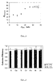
- Fig. 2 Collection efficiency of VPD-DC applied on multi-element spin coated Ge wafers using a 37% HCl or 47% HBr DC solution.
- Fig. 3 (a): Influence of the HCl concentration and wafer temperature on the removal of the Ge matrix and (b) related TXRF detection efficiency of traces (K, Ca, Sc, Cr, Fe, Ni, Zn all at 2.5E12 atoms)
- an impurity measuring method for Ge wafers comprising the steps of:
- Said method is of particular importance for measuring metallic contamination on the surface of Ge substrates.
- said Ge-phobic solution comprises HCl or HBr or any combination thereof.
- said solution comprises at least 30 wt.% HCl or at least 30 wt.% HBr or any combination thereof.
- the solution comprises HCl or HBr or any combination thereof and less then 0,25 wt.% H 2 O 2 .
- said Ge-phobic solution comprises 37 wt.% HCl.
- an impurity measuring method for Ge wafers comprising the steps as disclosed in the first aspect of this invention and an additional step making the surface of a Ge substrate phobic to said impurity collecting solution, using a vapor of a second solution.
- said Ge-phobic solution comprises HCl or HBr or any combination thereof.
- said solution comprises at least 30 wt.% HCl or at least 30 wt.% HBr or any combination thereof.
- the solution comprises HCl or HBr or any combination thereof and less then 0,25 wt.% H 2 O 2 .
- said Ge-phobic solution comprises 37 wt.% HCl.
- said second solution is of the form HX, in which X is F, Cl, or Br.
- the present invention provides a method for measuring an impurity upon the surface of a substrate, comprising (or consisting of) the steps of:
- substrate essentially/substantially of Ge refers to a germanium substrate (Ge substrate), which may have on its surface native germanium oxides
- Ge substrate may also refer to a substrate essentially of Ge.
- phobic solution refers to a solution that does not wet the Ge surface (or which is not absorbed by the Ge substrate). Consequently, the droplet of said solution can be used to scan the Ge surface.
- said first solution also referred to as Ge-phobic solution, comprises HCl and/or HBr.
- said Ge-phobic solution comprises:
- the contact angle can be increased significantly up to 55 degrees by addition of HCl or HBr or any combination thereof to an aqueous phase.
- Figure 1 shows the contact angle values versus the concentration of HCl in the micro-droplet after a HF VPD treatment. From about 20 wt.%, from about 25 wt.%, or from about 30 wt% HCl, the contact angle reaches values of at least 50 degrees.
- the contact angle reaches values of at least 50 degrees.
- a preferred Ge-phobic solution comprises at least about 37 wt.% HCl or at least about 47 wt.% HBr.
- a Ge-phobic solution of the invention may further comprise less then about 0,25 wt.% H 2 O 2 , or may be free of germanium oxidizing compounds.
- Ge oxidizing compounds in combination with the aqueous phase cause severe Ge etching.
- These Ge oxidizing compounds may be H 2 O 2 , HNO 3 , O 2 , O 3 , or any compound forming germanium oxides.
- the present invention provides a method for measuring an impurity upon the surface of a Ge substrate comprising (or consisting of) the steps of:
- the movement of the drop may occur at a speed of lower than about 20 mm/s, lower than about 10 mm/s, or about 5 mm/s.
- the analysis of the recovered drop may be performed by any wet chemical micro trace analytical technique such as Graphite Furnace - Atomic Absorption Spectrometry (GF-AAS) or Inductive Coupled Plasma - Mass Spectrometry (ICP-MS).
- GF-AAS Graphite Furnace - Atomic Absorption Spectrometry
- ICP-MS Inductive Coupled Plasma - Mass Spectrometry
- the micro-droplet is dried on a carrier substrate and the resulted residue is analyzed by TXRF.
- a method according to the invention may comprise, before the dropping step, an additional step of treating the surface of a Ge substrate with a second solution in form of vapor, for etching, at least partially, the native germanium oxides.
- Said second solution also referred to as VPD-solution, preferably comprise a halogen.
- said second solution may comprise HF, HCl or HBr or any combination thereof.
- the surface of a Ge substrate is rendered more phobic to the phobic solution.
- Figure 2 shows collection efficiency values are very close to unity for all of the investigated elements.
- the Ge matrix may be removed at least partially. This may occur by chemical reaction with HCl and/or HBr, preferably followed by a heating step.
- the VPD-DC step results in a micro-droplet containing a large Ge matrix concentration of typically 10 16 -10 17 atoms (i.e. 100-1000 mg/L). This high matrix concentration can affect the analysis of ultra-traces of contaminants within this matrix. Therefore the Ge matrix is preferably removed at least partially, prior to the analysis.
- the Si matrix is removed by a selective volatilization of SiF 4 during the dry step.
- Ge can however not be removed from aqueous solutions under speciation of GeF 4 but must be removed as the volatile GeCl 4 or GeBr 4 . These compounds can be formed in a reaction with HCl and/or HBr. Consequently, during droplet collection using HCl and/or HBr solutions, the Ge matrix reacts already with HCl and/or HBr, resulting in the volatile product, which then is removed by heating the micro-droplet.
- a method according to the invention further comprises, before or during the analysing step, the step of removing the Ge present in the drop (also referred to herein as "Ge matrix”), at least partially, by chemical reaction with HCl and/or HBr.
- a method of the invention further comprises, before or during the analysing step, the optional step of adding a solution of HCl and/or HBr to the drop, and the step of heating the drop.
- Figure 3 indicates that drying of a Ge containing micro-droplet on a hotplate yields a high Ge matrix removal for HCl concentrations of 2 wt.% or higher. Starting with a Ge amount of 4 ⁇ 10 16 atoms in the 50 ⁇ L droplet, the residual Ge concentration in the residue is decreased with more than three orders of magnitude.
- the method can be applied in a large temperature window temperature of 60-90°C.
- a method according to the invention allows the evaluation of the cleanliness of Ge wafers in a practical and very sensitive manner and should facilitate the development of cleaning recipes.
- Ge droplet residues standards were prepared by the micro-droplet deposition method.
- Standard multi-element solutions with a constant concentration of traces (K, Sc, Cr, Fe, Ni, Zn, all at 2.5x10¹² atoms/50 ⁇ L) and a variable Ge concentration were prepared by dilution of ICP-MS calibration standards (1000 ⁇ g/mL, nitrate salts, Merck).
- Droplets of 50 ⁇ L volume were pipetted on hydrophobic Si wafers (contact angle 65 deg) and dried at 50° C and 100 mbar in a Wafer Surface Preparation System (GeMeTec).
- the accuracy of a TXRF measurement was evaluated as the ratio of the measured amount of traces over the theoretical amount expected from the dilution of the standard solution.
- the spin coating technique was used to prepare standard wafers.
- Multi-element solutions were prepared by dilution of ICP-MS calibration standards (1000 mg/L, nitrate salts, Merck), acidified with HCl (2 vol% of 37% HCl, Ultrex, Baker).
- Portions of 10 mL were pipetted onto the Ge wafers positioned on a high-speed wafer spinner (Laurell WS-400). After 30 seconds, the spinner was run at 3000 rpm for 1 min in order to dry the wafer surface. With this procedure wafers with a target concentration in the order of 1 ⁇ 10 11 -1 ⁇ 10 12 at/cm 2 were prepared.
- a Ge standard solution has been prepared in ultra pure water.
- a Ge wafer piece was etched in a diluted H 2 O 2 solution (1/4 H 2 O 2 (30%, Ashland)/H 2 O) and the etched Ge amount was determined from differential weighing. Trace amounts of K, Ca, Sc, Cr, Fe, Ni and Zn) were added from a dilution of ICP-MS standard solutions (1000 mg/L, nitrate salts, Merck).
- TXRF analysis was performed using a FEI (formerly ATOMIKA) 8300 W system equipped with a W or Mo tube operated at 50 kV and 55 mA.
- the VPD-DC preparation was done using an automated Wafer Surface Preparation System (GeMeTec).
- the DC step was performed using a 50 ⁇ L droplet of HCl (37%, Ashland, Megabit) which scanned the wafer surface twice.
Landscapes
- Physics & Mathematics (AREA)
- Health & Medical Sciences (AREA)
- Life Sciences & Earth Sciences (AREA)
- Chemical & Material Sciences (AREA)
- Analytical Chemistry (AREA)
- Biochemistry (AREA)
- General Health & Medical Sciences (AREA)
- General Physics & Mathematics (AREA)
- Immunology (AREA)
- Pathology (AREA)
- Testing Or Measuring Of Semiconductors Or The Like (AREA)
Abstract
Description
- dropping a drop of a first solution on said surface to be measured,
- moving the drop dropped on said surface so that the drop is kept in contact with said surface and collects an impurity absorbed on said surface,
- recovering the drop after the movement, and
- analyzing the recovered drop by chemical analysis to determine the type and concentration of the impurity,
- dropping a drop of a solution on the surface of a Ge substrate to be measured, in which said solution is phobic to said Ge substrate;
- moving said drop dropped on the surface of said Ge substrate so that said drop is kept in contact with the surface of said Ge substrate and collects an impurity on the surface of said Ge substrate;
- recovering said drop after the movement; and
- analyzing said recovered drop by chemical analysis to determine the type and concentration of an impurity on the surface of said Ge substrate.
- dropping a drop of a first solution on said surface to be measured,
- moving the drop dropped on said surface so that the drop is kept in contact with said surface and collects an impurity absorbed on said surface,
- recovering the drop after the movement, and
- analyzing the recovered drop by chemical analysis to determine the type and concentration of the impurity,
- HCl in a concentration of at least about 20 wt.%, preferably of at least about 25 wt.%, more preferably of at least about 30 wt.%, or at least about 35 wt.%,
- HBr in a concentration of at least about 20 wt.%, preferably of at least about 25 wt.%, more preferably of at least about 30 wt.%, or at least about 35 wt.%, or
- HCl and HBr in a concentration of at least about 20 wt.% (total halogen concentration), preferably of at least about 25 wt.%, more preferably of at least about 30 wt.%, or at least about 35 wt.%.
- dropping a drop of a solution comprising HCl and/or HBr in a concentration of at least 20 wt.%, preferably of at least 25 wt.%, more preferably of at least 30 wt.%, in particular of (about) 37 wt.%, on said surface,
- moving the drop dropped on said surface so that the drop is kept in contact with said surface and collects an impurity absorbed on said surface,
- recovering the drop after the movement, and
- analyzing the recovered drop by chemical analysis to determine the type and concentration of the impurity.
Claims (12)
- A method for measuring an impurity upon the surface of a substrate comprising the steps of:characterized in that the substrate consists essentially of Ge, and in that the first solution is phobic to Ge substrate.dropping a drop of a first solution on said surface to be measured,moving the drop dropped on said surface so that the drop is kept in contact with said surface and collects an impurity absorbed on said surface,recovering the drop after the movement, andanalyzing the recovered drop by chemical analysis to determine the type and concentration of the impurity,
- A method according to claim 1, wherein said first solution comprises HCl and/or HBr.
- A method according to claim 2, wherein HCl and/or HBr is/are in a concentration of at least 30 wt.%, or at least 35 wt.%.
- A method according to claim 2 or 3, wherein said first solution comprises 37 wt.% HCl.
- A method according to claim 2 or 3, wherein said first solution comprises 47 wt.% HBr.
- A method according to any of claims 1 to 5, wherein said first solution further comprises less than 0,25 wt.% H2O2.
- A method according to claim 6, wherein said first solution is free of germanium oxidizing compounds.
- A method according to any of claims 1 to 7, further comprising, before said dropping step, the step of etching said surface.
- A method according to claim 8, wherein said etching step is performed with a second solution comprising HF, HCl or HBr or any combination thereof.
- A method according to any of claims 1 to 9, wherein the Ge present in said drop is removed, at least partially, by chemical reaction with HCl and/or HBr.
- A method according to any of claims 1 to 9, further comprising, before or during said analyzing step, optionally the step of adding a HCl and/or HBr solution to the drop, and the step of heating said drop.
- A method according to any of claims 1 to 11, wherein said impurity is any metal.
Applications Claiming Priority (2)
| Application Number | Priority Date | Filing Date | Title |
|---|---|---|---|
| US53021403P | 2003-12-12 | 2003-12-12 | |
| US530214P | 2003-12-12 |
Publications (2)
| Publication Number | Publication Date |
|---|---|
| EP1542006A1 true EP1542006A1 (en) | 2005-06-15 |
| EP1542006B1 EP1542006B1 (en) | 2015-02-11 |
Family
ID=34520281
Family Applications (1)
| Application Number | Title | Priority Date | Filing Date |
|---|---|---|---|
| EP04447274.4A Expired - Lifetime EP1542006B1 (en) | 2003-12-12 | 2004-12-13 | Impurity measuring method for GE substrates |
Country Status (2)
| Country | Link |
|---|---|
| US (1) | US7399635B2 (en) |
| EP (1) | EP1542006B1 (en) |
Families Citing this family (3)
| Publication number | Priority date | Publication date | Assignee | Title |
|---|---|---|---|---|
| JP4804950B2 (en) * | 2005-09-26 | 2011-11-02 | 東京応化工業株式会社 | Method for measuring immersion lithography dissolved component of organic film |
| JP4992246B2 (en) * | 2006-02-22 | 2012-08-08 | 株式会社Sumco | Method for evaluating Cu in silicon wafer |
| US7732225B2 (en) * | 2006-06-29 | 2010-06-08 | Texas Instruments Incorporated | Method for measuring contamination in liquids at PPQ levels |
Citations (1)
| Publication number | Priority date | Publication date | Assignee | Title |
|---|---|---|---|---|
| EP0339463A2 (en) * | 1988-04-25 | 1989-11-02 | Kabushiki Kaisha Toshiba | Impurity measuring method and apparatus |
Family Cites Families (4)
| Publication number | Priority date | Publication date | Assignee | Title |
|---|---|---|---|---|
| US3979240A (en) * | 1975-05-02 | 1976-09-07 | General Electric Company | Method of etching indium tin oxide |
| US6620632B2 (en) * | 2000-04-06 | 2003-09-16 | Seh America, Inc. | Method for evaluating impurity concentrations in semiconductor substrates |
| JP2003086554A (en) * | 2001-09-11 | 2003-03-20 | Mitsubishi Heavy Ind Ltd | Apparatus and method for manufacturing semiconductor substrate |
| US6864190B2 (en) * | 2002-10-17 | 2005-03-08 | National Research Council Of Canada | Laser chemical fabrication of nanostructures |
-
2004
- 2004-12-10 US US11/009,096 patent/US7399635B2/en active Active
- 2004-12-13 EP EP04447274.4A patent/EP1542006B1/en not_active Expired - Lifetime
Patent Citations (1)
| Publication number | Priority date | Publication date | Assignee | Title |
|---|---|---|---|---|
| EP0339463A2 (en) * | 1988-04-25 | 1989-11-02 | Kabushiki Kaisha Toshiba | Impurity measuring method and apparatus |
Non-Patent Citations (4)
| Title |
|---|
| "Chemical analysis of ultratrace impurities in SIO2 films", JAPANESE JOURNAL OF APPLIED PHYSICS, PUBLICATION OFFICE JAPANESE JOURNAL OF APPLIED PHYSICS. TOKYO, JP, 30 September 1984 (1984-09-30), pages 281 - 284, XP002138722, ISSN: 0021-4922 * |
| D. HELLIN ET AL: "Determination of metallic contaminants on Ge wafers using direct- and droplet sandwich etch-total reflection X-ray fluorescence spectrometry", SPECTROCHIMICA ACTA PART B, vol. 58, no. 12, 9 December 2003 (2003-12-09), pages 2093 - 2104, XP002323124 * |
| MCDANIEL F D ET AL: "Impurity measurements in semiconductor materials using trace element accelerator mass spectrometry", NUCLEAR INSTRUMENTS & METHODS IN PHYSICS RESEARCH, SECTION - B: BEAM INTERACTIONS WITH MATERIALS AND ATOMS, NORTH-HOLLAND PUBLISHING COMPANY. AMSTERDAM, NL, vol. 190, no. 1-4, May 2002 (2002-05-01), pages 826 - 830, XP004351657, ISSN: 0168-583X * |
| S. PAHLKE ET AL: "Determination of ultra trace contaminants on silicon wafer surfaces using total-reflection X.ray fluorescence TXRF 'state-of-the-art'", SPECTROCHIMICA ACTA PART B, vol. 56, no. 11, 30 November 2001 (2001-11-30), pages 2261 - 2274, XP002323125 * |
Also Published As
| Publication number | Publication date |
|---|---|
| EP1542006B1 (en) | 2015-02-11 |
| US20050170524A1 (en) | 2005-08-04 |
| US7399635B2 (en) | 2008-07-15 |
Similar Documents
| Publication | Publication Date | Title |
|---|---|---|
| KR101868775B1 (en) | Silicon substrate analyzing device | |
| JP3249316B2 (en) | Surface treatment method for a subject to be subjected to total reflection X-ray fluorescence analysis | |
| KR101242246B1 (en) | Apparatus for measuring impurities on wafer and Method for measuring impurities on wafer | |
| JP6118031B2 (en) | Impurity analysis apparatus and method | |
| US20070207616A1 (en) | Method for assaying copper in silicon wafers | |
| JP2019078684A (en) | Silicon wafer metal impurity analysis method | |
| US11742230B2 (en) | Contaminant detection tools including nebulizer and related methods | |
| Fucskó et al. | Measurement of Trace Metallic Contaminants on Silicon Wafer Surfaces in Native and Dielectric Silicon Oxides by Vapor Phase Decomposition Flow Injection Inductively Coupled Plasma‐Mass Spectrometry | |
| EP1542006B1 (en) | Impurity measuring method for GE substrates | |
| Ferrero et al. | Improving the detection limits for vapor phase decomposition-inductively coupled plasma mass spectrometry (VPD-ICP-MS) analysis | |
| JP2002368052A (en) | Method for desorbing silicon and method for analyzing impurities in silicon wafer | |
| CN205786470U (en) | Substrate analytical equipment | |
| US6911096B2 (en) | Method of collecting impurities on surface of semiconductor wafer | |
| JP2001242052A (en) | Method for analyzing impurities in semiconductor substrates or chemicals | |
| Buhrer | Application of vapor phase decomposition/total reflection X-ray fluorescence in the silicon semiconductor manufacturing environment | |
| Hellin et al. | Determination of metallic contaminants on Ge wafers using direct-and droplet sandwich etch-total reflection X-ray fluorescence spectrometry | |
| Hellin et al. | Remediation for TXRF saturation effects on microdroplet residues from preconcentration methods on semiconductor wafers | |
| US6146909A (en) | Detecting trace levels of copper | |
| Hellin et al. | Vapor phase decomposition–droplet collection–total reflection X-ray fluorescence spectrometry for metallic contamination analysis on Ge wafers | |
| JP2950310B2 (en) | Method for analyzing metal impurities on semiconductor substrate surface and substrate | |
| Ichikawa et al. | Analysis of metallic impurities in Si wafers using fully automated VPD ICP-MS | |
| Hellin et al. | VPD-DC-TXRF for metallic contamination analysis of Ge wafers | |
| KR100772280B1 (en) | Elemental Analysis of Optical, Electronic or Optoelectronic Substrates | |
| Wang et al. | Analytical techniques for trace elemental analyses on wafer surfaces for monitoring and controlling contamination | |
| JPH10332554A (en) | Surface impurity measurement method |
Legal Events
| Date | Code | Title | Description |
|---|---|---|---|
| PUAI | Public reference made under article 153(3) epc to a published international application that has entered the european phase |
Free format text: ORIGINAL CODE: 0009012 |
|
| AK | Designated contracting states |
Kind code of ref document: A1 Designated state(s): AT BE BG CH CY CZ DE DK EE ES FI FR GB GR HU IE IS IT LI LT LU MC NL PL PT RO SE SI SK TR |
|
| AX | Request for extension of the european patent |
Extension state: AL BA HR LV MK YU |
|
| 17P | Request for examination filed |
Effective date: 20051103 |
|
| RAP1 | Party data changed (applicant data changed or rights of an application transferred) |
Owner name: UMICORE |
|
| RAP1 | Party data changed (applicant data changed or rights of an application transferred) |
Owner name: INTERUNIVERSITAIR MICROELEKTRONICA CENTRUM VZW (IM Owner name: UMICORE |
|
| AKX | Designation fees paid |
Designated state(s): AT BE BG CH CY CZ DE DK EE ES FI FR GB GR HU IE IS IT LI LT LU MC NL PL PT RO SE SI SK TR |
|
| RAP1 | Party data changed (applicant data changed or rights of an application transferred) |
Owner name: UMICORE Owner name: IMEC |
|
| 17Q | First examination report despatched |
Effective date: 20120917 |
|
| REG | Reference to a national code |
Ref country code: DE Ref legal event code: R079 Ref document number: 602004046602 Country of ref document: DE Free format text: PREVIOUS MAIN CLASS: G01N0031000000 Ipc: G01N0001020000 |
|
| GRAP | Despatch of communication of intention to grant a patent |
Free format text: ORIGINAL CODE: EPIDOSNIGR1 |
|
| RIC1 | Information provided on ipc code assigned before grant |
Ipc: G01N 1/38 20060101ALI20140704BHEP Ipc: G01N 1/02 20060101AFI20140704BHEP |
|
| INTG | Intention to grant announced |
Effective date: 20140722 |
|
| GRAS | Grant fee paid |
Free format text: ORIGINAL CODE: EPIDOSNIGR3 |
|
| GRAA | (expected) grant |
Free format text: ORIGINAL CODE: 0009210 |
|
| AK | Designated contracting states |
Kind code of ref document: B1 Designated state(s): AT BE BG CH CY CZ DE DK EE ES FI FR GB GR HU IE IS IT LI LT LU MC NL PL PT RO SE SI SK TR |
|
| REG | Reference to a national code |
Ref country code: GB Ref legal event code: FG4D |
|
| REG | Reference to a national code |
Ref country code: CH Ref legal event code: EP |
|
| REG | Reference to a national code |
Ref country code: IE Ref legal event code: FG4D |
|
| REG | Reference to a national code |
Ref country code: AT Ref legal event code: REF Ref document number: 710078 Country of ref document: AT Kind code of ref document: T Effective date: 20150315 |
|
| REG | Reference to a national code |
Ref country code: DE Ref legal event code: R096 Ref document number: 602004046602 Country of ref document: DE Effective date: 20150326 |
|
| REG | Reference to a national code |
Ref country code: NL Ref legal event code: VDEP Effective date: 20150211 |
|
| REG | Reference to a national code |
Ref country code: AT Ref legal event code: MK05 Ref document number: 710078 Country of ref document: AT Kind code of ref document: T Effective date: 20150211 |
|
| REG | Reference to a national code |
Ref country code: LT Ref legal event code: MG4D |
|
| PG25 | Lapsed in a contracting state [announced via postgrant information from national office to epo] |
Ref country code: FI Free format text: LAPSE BECAUSE OF FAILURE TO SUBMIT A TRANSLATION OF THE DESCRIPTION OR TO PAY THE FEE WITHIN THE PRESCRIBED TIME-LIMIT Effective date: 20150211 Ref country code: ES Free format text: LAPSE BECAUSE OF FAILURE TO SUBMIT A TRANSLATION OF THE DESCRIPTION OR TO PAY THE FEE WITHIN THE PRESCRIBED TIME-LIMIT Effective date: 20150211 Ref country code: SE Free format text: LAPSE BECAUSE OF FAILURE TO SUBMIT A TRANSLATION OF THE DESCRIPTION OR TO PAY THE FEE WITHIN THE PRESCRIBED TIME-LIMIT Effective date: 20150211 Ref country code: LT Free format text: LAPSE BECAUSE OF FAILURE TO SUBMIT A TRANSLATION OF THE DESCRIPTION OR TO PAY THE FEE WITHIN THE PRESCRIBED TIME-LIMIT Effective date: 20150211 |
|
| PG25 | Lapsed in a contracting state [announced via postgrant information from national office to epo] |
Ref country code: IS Free format text: LAPSE BECAUSE OF FAILURE TO SUBMIT A TRANSLATION OF THE DESCRIPTION OR TO PAY THE FEE WITHIN THE PRESCRIBED TIME-LIMIT Effective date: 20150611 Ref country code: NL Free format text: LAPSE BECAUSE OF FAILURE TO SUBMIT A TRANSLATION OF THE DESCRIPTION OR TO PAY THE FEE WITHIN THE PRESCRIBED TIME-LIMIT Effective date: 20150211 Ref country code: GR Free format text: LAPSE BECAUSE OF FAILURE TO SUBMIT A TRANSLATION OF THE DESCRIPTION OR TO PAY THE FEE WITHIN THE PRESCRIBED TIME-LIMIT Effective date: 20150512 Ref country code: AT Free format text: LAPSE BECAUSE OF FAILURE TO SUBMIT A TRANSLATION OF THE DESCRIPTION OR TO PAY THE FEE WITHIN THE PRESCRIBED TIME-LIMIT Effective date: 20150211 |
|
| PG25 | Lapsed in a contracting state [announced via postgrant information from national office to epo] |
Ref country code: EE Free format text: LAPSE BECAUSE OF FAILURE TO SUBMIT A TRANSLATION OF THE DESCRIPTION OR TO PAY THE FEE WITHIN THE PRESCRIBED TIME-LIMIT Effective date: 20150211 Ref country code: CZ Free format text: LAPSE BECAUSE OF FAILURE TO SUBMIT A TRANSLATION OF THE DESCRIPTION OR TO PAY THE FEE WITHIN THE PRESCRIBED TIME-LIMIT Effective date: 20150211 Ref country code: RO Free format text: LAPSE BECAUSE OF FAILURE TO SUBMIT A TRANSLATION OF THE DESCRIPTION OR TO PAY THE FEE WITHIN THE PRESCRIBED TIME-LIMIT Effective date: 20150211 Ref country code: DK Free format text: LAPSE BECAUSE OF FAILURE TO SUBMIT A TRANSLATION OF THE DESCRIPTION OR TO PAY THE FEE WITHIN THE PRESCRIBED TIME-LIMIT Effective date: 20150211 Ref country code: SK Free format text: LAPSE BECAUSE OF FAILURE TO SUBMIT A TRANSLATION OF THE DESCRIPTION OR TO PAY THE FEE WITHIN THE PRESCRIBED TIME-LIMIT Effective date: 20150211 |
|
| REG | Reference to a national code |
Ref country code: DE Ref legal event code: R097 Ref document number: 602004046602 Country of ref document: DE |
|
| REG | Reference to a national code |
Ref country code: FR Ref legal event code: PLFP Year of fee payment: 12 |
|
| PG25 | Lapsed in a contracting state [announced via postgrant information from national office to epo] |
Ref country code: PL Free format text: LAPSE BECAUSE OF FAILURE TO SUBMIT A TRANSLATION OF THE DESCRIPTION OR TO PAY THE FEE WITHIN THE PRESCRIBED TIME-LIMIT Effective date: 20150211 |
|
| PLBE | No opposition filed within time limit |
Free format text: ORIGINAL CODE: 0009261 |
|
| STAA | Information on the status of an ep patent application or granted ep patent |
Free format text: STATUS: NO OPPOSITION FILED WITHIN TIME LIMIT |
|
| PG25 | Lapsed in a contracting state [announced via postgrant information from national office to epo] |
Ref country code: IT Free format text: LAPSE BECAUSE OF FAILURE TO SUBMIT A TRANSLATION OF THE DESCRIPTION OR TO PAY THE FEE WITHIN THE PRESCRIBED TIME-LIMIT Effective date: 20150211 |
|
| 26N | No opposition filed |
Effective date: 20151112 |
|
| PG25 | Lapsed in a contracting state [announced via postgrant information from national office to epo] |
Ref country code: SI Free format text: LAPSE BECAUSE OF FAILURE TO SUBMIT A TRANSLATION OF THE DESCRIPTION OR TO PAY THE FEE WITHIN THE PRESCRIBED TIME-LIMIT Effective date: 20150211 |
|
| PG25 | Lapsed in a contracting state [announced via postgrant information from national office to epo] |
Ref country code: BE Free format text: LAPSE BECAUSE OF FAILURE TO SUBMIT A TRANSLATION OF THE DESCRIPTION OR TO PAY THE FEE WITHIN THE PRESCRIBED TIME-LIMIT Effective date: 20150211 |
|
| PG25 | Lapsed in a contracting state [announced via postgrant information from national office to epo] |
Ref country code: MC Free format text: LAPSE BECAUSE OF FAILURE TO SUBMIT A TRANSLATION OF THE DESCRIPTION OR TO PAY THE FEE WITHIN THE PRESCRIBED TIME-LIMIT Effective date: 20150211 Ref country code: LU Free format text: LAPSE BECAUSE OF FAILURE TO SUBMIT A TRANSLATION OF THE DESCRIPTION OR TO PAY THE FEE WITHIN THE PRESCRIBED TIME-LIMIT Effective date: 20151213 |
|
| REG | Reference to a national code |
Ref country code: CH Ref legal event code: PL |
|
| GBPC | Gb: european patent ceased through non-payment of renewal fee |
Effective date: 20151213 |
|
| REG | Reference to a national code |
Ref country code: IE Ref legal event code: MM4A |
|
| PG25 | Lapsed in a contracting state [announced via postgrant information from national office to epo] |
Ref country code: IE Free format text: LAPSE BECAUSE OF NON-PAYMENT OF DUE FEES Effective date: 20151213 Ref country code: CH Free format text: LAPSE BECAUSE OF NON-PAYMENT OF DUE FEES Effective date: 20151231 Ref country code: LI Free format text: LAPSE BECAUSE OF NON-PAYMENT OF DUE FEES Effective date: 20151231 Ref country code: GB Free format text: LAPSE BECAUSE OF NON-PAYMENT OF DUE FEES Effective date: 20151213 |
|
| REG | Reference to a national code |
Ref country code: FR Ref legal event code: PLFP Year of fee payment: 13 |
|
| PG25 | Lapsed in a contracting state [announced via postgrant information from national office to epo] |
Ref country code: BG Free format text: LAPSE BECAUSE OF FAILURE TO SUBMIT A TRANSLATION OF THE DESCRIPTION OR TO PAY THE FEE WITHIN THE PRESCRIBED TIME-LIMIT Effective date: 20150211 Ref country code: HU Free format text: LAPSE BECAUSE OF FAILURE TO SUBMIT A TRANSLATION OF THE DESCRIPTION OR TO PAY THE FEE WITHIN THE PRESCRIBED TIME-LIMIT; INVALID AB INITIO Effective date: 20041213 |
|
| PG25 | Lapsed in a contracting state [announced via postgrant information from national office to epo] |
Ref country code: CY Free format text: LAPSE BECAUSE OF FAILURE TO SUBMIT A TRANSLATION OF THE DESCRIPTION OR TO PAY THE FEE WITHIN THE PRESCRIBED TIME-LIMIT Effective date: 20150211 |
|
| PG25 | Lapsed in a contracting state [announced via postgrant information from national office to epo] |
Ref country code: TR Free format text: LAPSE BECAUSE OF FAILURE TO SUBMIT A TRANSLATION OF THE DESCRIPTION OR TO PAY THE FEE WITHIN THE PRESCRIBED TIME-LIMIT Effective date: 20150211 |
|
| REG | Reference to a national code |
Ref country code: FR Ref legal event code: PLFP Year of fee payment: 14 |
|
| PG25 | Lapsed in a contracting state [announced via postgrant information from national office to epo] |
Ref country code: PT Free format text: LAPSE BECAUSE OF FAILURE TO SUBMIT A TRANSLATION OF THE DESCRIPTION OR TO PAY THE FEE WITHIN THE PRESCRIBED TIME-LIMIT Effective date: 20150211 |
|
| PGFP | Annual fee paid to national office [announced via postgrant information from national office to epo] |
Ref country code: DE Payment date: 20191119 Year of fee payment: 16 |
|
| PGFP | Annual fee paid to national office [announced via postgrant information from national office to epo] |
Ref country code: FR Payment date: 20191120 Year of fee payment: 16 |
|
| REG | Reference to a national code |
Ref country code: DE Ref legal event code: R119 Ref document number: 602004046602 Country of ref document: DE |
|
| PG25 | Lapsed in a contracting state [announced via postgrant information from national office to epo] |
Ref country code: FR Free format text: LAPSE BECAUSE OF NON-PAYMENT OF DUE FEES Effective date: 20201231 |
|
| PG25 | Lapsed in a contracting state [announced via postgrant information from national office to epo] |
Ref country code: DE Free format text: LAPSE BECAUSE OF NON-PAYMENT OF DUE FEES Effective date: 20210701 |