EP1541528A1 - Quasi-one-dimensional polymers based on the metal-chalcogen-halogen system - Google Patents
Quasi-one-dimensional polymers based on the metal-chalcogen-halogen system Download PDFInfo
- Publication number
- EP1541528A1 EP1541528A1 EP03028188A EP03028188A EP1541528A1 EP 1541528 A1 EP1541528 A1 EP 1541528A1 EP 03028188 A EP03028188 A EP 03028188A EP 03028188 A EP03028188 A EP 03028188A EP 1541528 A1 EP1541528 A1 EP 1541528A1
- Authority
- EP
- European Patent Office
- Prior art keywords
- material according
- chalcogen
- elements
- transition metal
- synthesis
- Prior art date
- Legal status (The legal status is an assumption and is not a legal conclusion. Google has not performed a legal analysis and makes no representation as to the accuracy of the status listed.)
- Withdrawn
Links
Images


Classifications
-
- C—CHEMISTRY; METALLURGY
- C01—INORGANIC CHEMISTRY
- C01G—COMPOUNDS CONTAINING METALS NOT COVERED BY SUBCLASSES C01D OR C01F
- C01G1/00—Methods of preparing compounds of metals not covered by subclasses C01B, C01C, C01D, or C01F, in general
-
- B—PERFORMING OPERATIONS; TRANSPORTING
- B82—NANOTECHNOLOGY
- B82Y—SPECIFIC USES OR APPLICATIONS OF NANOSTRUCTURES; MEASUREMENT OR ANALYSIS OF NANOSTRUCTURES; MANUFACTURE OR TREATMENT OF NANOSTRUCTURES
- B82Y30/00—Nanotechnology for materials or surface science, e.g. nanocomposites
-
- C—CHEMISTRY; METALLURGY
- C01—INORGANIC CHEMISTRY
- C01G—COMPOUNDS CONTAINING METALS NOT COVERED BY SUBCLASSES C01D OR C01F
- C01G39/00—Compounds of molybdenum
-
- C—CHEMISTRY; METALLURGY
- C01—INORGANIC CHEMISTRY
- C01G—COMPOUNDS CONTAINING METALS NOT COVERED BY SUBCLASSES C01D OR C01F
- C01G39/00—Compounds of molybdenum
- C01G39/006—Compounds containing molybdenum, with or without oxygen or hydrogen, and containing two or more other elements
-
- C—CHEMISTRY; METALLURGY
- C01—INORGANIC CHEMISTRY
- C01G—COMPOUNDS CONTAINING METALS NOT COVERED BY SUBCLASSES C01D OR C01F
- C01G41/00—Compounds of tungsten
-
- C—CHEMISTRY; METALLURGY
- C01—INORGANIC CHEMISTRY
- C01G—COMPOUNDS CONTAINING METALS NOT COVERED BY SUBCLASSES C01D OR C01F
- C01G41/00—Compounds of tungsten
- C01G41/006—Compounds containing tungsten, with or without oxygen or hydrogen, and containing two or more other elements
-
- H—ELECTRICITY
- H01—ELECTRIC ELEMENTS
- H01J—ELECTRIC DISCHARGE TUBES OR DISCHARGE LAMPS
- H01J9/00—Apparatus or processes specially adapted for the manufacture, installation, removal, maintenance of electric discharge tubes, discharge lamps, or parts thereof; Recovery of material from discharge tubes or lamps
- H01J9/02—Manufacture of electrodes or electrode systems
- H01J9/022—Manufacture of electrodes or electrode systems of cold cathodes
- H01J9/025—Manufacture of electrodes or electrode systems of cold cathodes of field emission cathodes
-
- B—PERFORMING OPERATIONS; TRANSPORTING
- B82—NANOTECHNOLOGY
- B82Y—SPECIFIC USES OR APPLICATIONS OF NANOSTRUCTURES; MEASUREMENT OR ANALYSIS OF NANOSTRUCTURES; MANUFACTURE OR TREATMENT OF NANOSTRUCTURES
- B82Y40/00—Manufacture or treatment of nanostructures
-
- C—CHEMISTRY; METALLURGY
- C01—INORGANIC CHEMISTRY
- C01P—INDEXING SCHEME RELATING TO STRUCTURAL AND PHYSICAL ASPECTS OF SOLID INORGANIC COMPOUNDS
- C01P2004/00—Particle morphology
- C01P2004/01—Particle morphology depicted by an image
- C01P2004/03—Particle morphology depicted by an image obtained by SEM
-
- C—CHEMISTRY; METALLURGY
- C01—INORGANIC CHEMISTRY
- C01P—INDEXING SCHEME RELATING TO STRUCTURAL AND PHYSICAL ASPECTS OF SOLID INORGANIC COMPOUNDS
- C01P2004/00—Particle morphology
- C01P2004/01—Particle morphology depicted by an image
- C01P2004/04—Particle morphology depicted by an image obtained by TEM, STEM, STM or AFM
-
- C—CHEMISTRY; METALLURGY
- C01—INORGANIC CHEMISTRY
- C01P—INDEXING SCHEME RELATING TO STRUCTURAL AND PHYSICAL ASPECTS OF SOLID INORGANIC COMPOUNDS
- C01P2004/00—Particle morphology
- C01P2004/10—Particle morphology extending in one dimension, e.g. needle-like
-
- C—CHEMISTRY; METALLURGY
- C01—INORGANIC CHEMISTRY
- C01P—INDEXING SCHEME RELATING TO STRUCTURAL AND PHYSICAL ASPECTS OF SOLID INORGANIC COMPOUNDS
- C01P2004/00—Particle morphology
- C01P2004/10—Particle morphology extending in one dimension, e.g. needle-like
- C01P2004/16—Nanowires or nanorods, i.e. solid nanofibres with two nearly equal dimensions between 1-100 nanometer
-
- C—CHEMISTRY; METALLURGY
- C01—INORGANIC CHEMISTRY
- C01P—INDEXING SCHEME RELATING TO STRUCTURAL AND PHYSICAL ASPECTS OF SOLID INORGANIC COMPOUNDS
- C01P2004/00—Particle morphology
- C01P2004/60—Particles characterised by their size
- C01P2004/64—Nanometer sized, i.e. from 1-100 nanometer
-
- C—CHEMISTRY; METALLURGY
- C01—INORGANIC CHEMISTRY
- C01P—INDEXING SCHEME RELATING TO STRUCTURAL AND PHYSICAL ASPECTS OF SOLID INORGANIC COMPOUNDS
- C01P2006/00—Physical properties of inorganic compounds
- C01P2006/80—Compositional purity
Definitions
- M transition metal
- C chalcogen
- H halogen
- y and z are real numbers such that 8.2 ⁇ ( y + z ) ⁇ 10.
- Carbon nanotubes as reported by Ijima have many functional properties, which makes them important in numerous different applications, ranging from nanoelectronics to components in composites, as chemical and nano-electromechanical sensors and various other devices (R.H.Baughman, A.A.Zakhidov and Walt A. de Heer, Science 297 (2002), 789).
- Carbon nanotubes are synthesised such that many different varieties of material are grown simultaneously, so that the nanotubes typically grow all of different diameters, chiralities and with different physical and electronic properties.
- metal catalysts in the synthesis strongly inhibits the separation of nanotubes without damage.
- the catalyst particles are typically covered with carbon layers, which also covalently bind to the nanotubes making separation exceedingly difficult. Also, the synthesis methods presently used, such as in an arc discharge or by laser ablation, are rather unsuitable for easy scaling up of production volume of monodisperse single-species nanotubes or nanowires.
- Inorganic nanotubes based on transition metal chalcogenides have been synthesised and proposed as a possible alternative to carbon nanotubes in many existing applications and some new ones.
- US-P-6,217,843, (Appl. No. 308663) and US-P-5,958,358 (Appl. No. 657431)) refer to a method of preparation of nano-particles of metal oxides and to metal-intercalated and/or metal caged "inorganic fullerene-like" structures of metal chalcogenides obtained therefrom fullerene-like structures of dichalcogenide nanotubes.
- the materials synthesized in this way are non-monodisperse, contain a small proportion of single-wall and multi-wall nanotubes with different diameters and divergent wall layer thicknesses, onion-like multi-layer fullerene structures and other materials.
- no catalyst particles are present, separation of the material synthesised in this way into specific components is difficult, and use of any one of the components is consequently very limited for many applications.
- the synthesis procedure described in the above patents involves multiple steps and cannot be easily performed by a single step process, making scaling up relatively difficult.
- Rem kar M. et al. (Science 292 (2001), 479-481) and PCT/SI01/00027 refer to the synthesis of quasi-one-dimensional nanostructures, called bundles of nanotubes in a fullerene-assisted transport reaction and have a formula MoS 2 I 1/3 .
- the synthesis of the material requires a transport reaction, which is relatively complex, and is not suitable applications where larger amounts of material are required.
- M 2 Mo 6 Se 6 Na, In, K, Tl
- These fibers are produced by two-step synthesis first of InMo 3 Se 3 and then oxidized in solution with HCl to give (Mo 3 Se 3 ) ⁇ fibers.
- the fibers produced this way can be stabilized by solvated ions in solution, but they are unstable in air and are not really suitable for applications as individual nanofibers or nanowires.
- a problem of the present invention is to provide improved materials, which may be used in a variety of different applications such as nano-electromechanical devices or sensors (NEMS).
- NEMS nano-electromechanical devices or sensors
- the present inventors surprisingly noted that when maintaining a ratio of the above indicated ingredients within the limits of 8.2 ⁇ (y+z) ⁇ 1 0 and performing the method of synthesis at a temperature exceeding 1000 °C, always materials showing a quasi three dimensional structure (i.e. being in the form of three dimensional crystals) are obtained which are air stable in contrast to prior art materials.
- the as-grown material structure are considered to represent bundles exhibiting a small diameter with 1-dimensional subunits, whose structure is wire-like at the molecular level, or bundles of one-dimensional polymers of Mo 6 S y I z clusters, or bundles composed of inorganic molecular wires.
- the materials have the advantages of advantages in that the bundles of (Mo 6 S y I z ) may be controllably dispersed into smaller ones, obtaining monodisperse dispersions of different diameters, the dispersed samples are stable in air and the synthesis of the material is straightforward (as compared e.g. to carbon nanotubes, which are functionally similar).
- the material obtained in this way does not contain no significant amounts of impurities, with the impurities still present not being chemically attached to the bundles of the material, while the as-grown wires may be longer than 1 mm, with sub-micron diameter.
- the compounds in the present invention differ from the known materials described in the first section by their stoichiometry and/or their composition.
- the materials are stable in air and may be prepared in suspensions in polar fluids, such as water as well as non-polar organic liquids. It may be used in applications for field emission tips, as lubricants, in nanoelectronics and batteries, as sensor templates etc., and can be doped with other alkali ions or molecules, with a wide range of potential applications.
- the material M is a transition metal selected from the group consisting of Mo, W, V, Ti, Ta, Nb, Zn, Hf, Re and Ru.
- C may be any chalcogen but is preferably sulfur, selenium or tellurium.
- H may be any halogen, but is preferably Iodine or Bromide.
- 8.2 ⁇ ( y + z) ⁇ 10 and preferably y + z 9.
- the invention relates to carbon nanotubes in that the form of growth and synthesis and preparation is such that it gives rise to similar appearance on the nanoscale. As is described by the terminology used in the field, the form of nanoropes, nanorods and nanowires.
- the present invention differs from the compounds described in the previous statement by the synthesis being performed above 1000 °C, surprisingly yielding quasi-one dimensional objects in the form of nanoneedles, nanorods, nanowires or nanowhiskers.
- the present invention also relates to previously known forms of transition metal chalcogenide halides different stoichiometry, namely 662 stoichiometry, such as Mo 6 Se 6 I 2 , which grow in the form of well-defined crystals. These materials have a well-defined crystal structure and also grow in the form of whiskers or rods.
- the present invention covers stoichiometries which differ from 662.
- the structural coherence is not present over distances more than 50 nm, arising from intrinsic reasons, such as bending or malleability of the material, which distinguishes the materials in this invention from crystalline whiskers or small crystals.
- the present invention relates to chain compounds with the formula M x C y such as Mo 2 S 3 which have a different stoichiometry.
- the present invention relates to a M x C y H z material such as MoS 2 I 1/3 which is grown in a modified transport reaction involving fullerenes such as C 60 and C 70 .
- the present invention refers to material which differs from compounds such as MoS 2 I 1/3 by the method of synthesis and by stoichiometry.
- the invention relates to items and devices, methods of making and using them and related systems on the scale of nanometers and micrometers.
- the present materials may be used in composites with enhanced mechanical, thermal or electrical properties, as battery electrodes, it may be with electrons or holes, as nanoconnectors, in nanodevices (e.g. FETs) in either metallic or semiconducting form depending on doping, connected to gold particles, as replacement material for carbon nanotubes, in applications which require one-dimensional structure or properties arising from confinement of electrons to one dimension, as field emission tips, as coatings, as catalyst, as superconductors, as carriers for functionalized sensors and detectors, as material utilising special chemical properties for attachment of various kinds of molecules or to surfaces, as solid-state lubricant and as additive material in liquid lubricants.
- nanodevices e.g. FETs
- the present materials may be embodied in a thin film or single rope, strand, needle, whisker or wire of said material deposited by evaporation of solvents, or electrodeposition including electrophoresis, dielectrophoresis etc. ,or in device made of single strands, multi-strand whiskers, ropes or rods of the Mo-S-I system, with items (i.e.
- Said structures which, when incorporated into devices using attached gold particles can form sensors, or on surfaces as films, used as an interface to temporary or permanent attachment of organic molecules via sulphur and/or carbon atom.
- the invention is embodied as a conducting or superconducting wire, or rope or rod or whisker, composed of smaller wires, etc. which range in diameter from 0.2 nanometers to 10 micrometers.
- Said structures which when dispersed into smaller bundles, ropes or individual tubes can act as lubricants, additives to lubricants, or components in composite materials in which friction can be reduced with or without the combination of increased strengths and/or enhanced electrical or thermal properties.
- the invention comprises the methods of growing, assembling and otherwise making articles and devices.
- a method of the invention involves growing rod-like, wire-like or rope-like objects composed of smaller quasi-one-dimensional subunits made of transition metal and chalcogen in various stoichiometry.
- the objects may contain also other doped atoms or ions, or interstitial atoms, ions or molecules including halogens, other transition metals, rare-earth metals, organic donors etc.
- the invention pertains to the synthesis of material under specific conditions above 1000 °C which has a particular shape of microrods, nanorods and nanowires, nanowhiskers, nanoropes, ranging in diameters from a few microns to a few nanometers.
- microrods, nanorods and nanowires are typically composite objects, composed of thin one-dimensional objects such as wires, strings or clusters of atoms arranged in straight or staggered chains or ladders.
- the invention is described as material whose wire-like or rod-like shape concentrates electric fields at their tips.
- the invention is described as a conducing nanowire, nanorope, nanorod, etc. of intertwined strands of smaller wires, strands ranging in diameter from 0.4 nm to 10000 nm.
- the synthesis is performed in a sealed and evacuated quartz ampoule having diameter of 19 mm and a length of 140 mm, (remaining gas pressure ⁇ 10 -3 torr) containing platelets of Mo sheet metal (Aldrich, molybdenum foil 0.1 mm thick, 99.9+%), S (Aldrich, sulfur powder, 99.98 %) and I 2 (Aldrich, 99.999+%) in the amounts 6:4:6 (Mo: 0.8925 g, S: 0.1988 g, I 2 : 1.1805 g).
- the ampoule is placed in a single-zone furnace ( LINDBERG STF 55346C) and heated from room temperature to a temperature of 1070 °C at a rate 8 K per hour.
- the composition as determined by EA (elemental analysis) is given as Mo 6 S 3 I 6 . found, %: Mo 40,4; S 6,4; I 53,1. (measurement tolerance ⁇ 0,2 - 0,3 %) calculated for Mo 6 S 3 I 6 , % : Mo 40,2; S 6,7; I 53,1.
- the structure of the material as grown is essentially crystalline in the usual sense. X-ray data shown rather broad peaks with no narrow well-defined sharp crystal peaks.
- the synthesis is performed in sealed and evacuated quartz ampoule (diameter 19 mm, length 140 mm), (remaining gas pressure ⁇ 10 -3 torr) containing platelets of Mo sheet metal (Aldrich, molybdenum foil 0.1 mm thick, 99.9+%), S (Aldrich, sulfur powder, 99.98 %) and I 2 (Aldrich, 99.999+%) in the amounts 6:4:4 (Mo: 0.8981 g, S: 0.2000 g, I 2 : 0.7919 g).
- the ampoule is placed in a single-zone furnace (LINDBERG STF 55346C) and heated from room temperature to a temperature of 1150 °C at a rate 8 K per hour.
- the composition, as determined EA (elemental analysis) is given as Mo6S 4.5 I 4.5 . found % Mo 43,5; S 11,2; I 45,3 (measure tolerance ⁇ 0,3%) calculated for Mo6S 4.5 I 4.5 , % Mo 44,6; S 11,2; I 44,2.
- the structure of the material as grown is not crystalline in the usual sense, particularly along the direction of the wires, because of the very weak forces in-between the wires.
- the microscopic structure cannot be described in terms of rolled-up sheets of layered dichalcogenide material, and cannot be described to be fullerene-like in structure.
- the morphology of the material is in the form of needles or ropes or wires, composed of small-diameter columnar structures.
- the material can be dispersed in a variety of solvents, such as isopropanol, methanol, water etc., using an ultrasonic bath, to various degrees, where the mean diameter of the nanowires thus obtained depends on the dilution and on the extent of sonification. Thinner diameters are obtained with more dilute solutions, and monodisperse dispersions of nanowires with mean diameter less than 4 nm can be obtained using this method with dilutions.
- solvents such as isopropanol, methanol, water etc.
- the materials are grown at temperatures above 1000 °C. Their stoichiometry is variable, and different compounds exist, which have different values y and z.
Landscapes
- Chemical & Material Sciences (AREA)
- Organic Chemistry (AREA)
- Inorganic Chemistry (AREA)
- Engineering & Computer Science (AREA)
- Nanotechnology (AREA)
- Materials Engineering (AREA)
- Condensed Matter Physics & Semiconductors (AREA)
- General Physics & Mathematics (AREA)
- Composite Materials (AREA)
- Crystallography & Structural Chemistry (AREA)
- Physics & Mathematics (AREA)
- Manufacturing & Machinery (AREA)
- Crystals, And After-Treatments Of Crystals (AREA)
- Inorganic Compounds Of Heavy Metals (AREA)
- Lubricants (AREA)
- Superconductors And Manufacturing Methods Therefor (AREA)
Abstract
Description
- The present invention relates to air-stable, monodisperse quasi-one-dimensional materials synthesised with sub-micron cross-section and described by the formula M6CyHz, wherein M = transition metal, C = chalcogen, H = halogen, and wherein y and z are real numbers such that 8.2 < (y+z) < 10. These materials may be synthesized in a single-step procedure at temperatures above 1000 °C. The present invention also concerns the use of these materials in electronic, chemical, optical or mechanical applications.
- Carbon nanotubes as reported by Ijima (I. Ijima, Nature 56 (1991), 354) have many functional properties, which makes them important in numerous different applications, ranging from nanoelectronics to components in composites, as chemical and nano-electromechanical sensors and various other devices (R.H.Baughman, A.A.Zakhidov and Walt A. de Heer, Science 297 (2002), 789). Carbon nanotubes are synthesised such that many different varieties of material are grown simultaneously, so that the nanotubes typically grow all of different diameters, chiralities and with different physical and electronic properties. Moreover the use of metal catalysts in the synthesis strongly inhibits the separation of nanotubes without damage. The catalyst particles are typically covered with carbon layers, which also covalently bind to the nanotubes making separation exceedingly difficult. Also, the synthesis methods presently used, such as in an arc discharge or by laser ablation, are rather unsuitable for easy scaling up of production volume of monodisperse single-species nanotubes or nanowires.
- Inorganic nanotubes based on transition metal chalcogenides have been synthesised and proposed as a possible alternative to carbon nanotubes in many existing applications and some new ones. US-P-6,217,843, (Appl. No. 308663) and US-P-5,958,358 (Appl. No. 657431)) refer to a method of preparation of nano-particles of metal oxides and to metal-intercalated and/or metal caged "inorganic fullerene-like" structures of metal chalcogenides obtained therefrom fullerene-like structures of dichalcogenide nanotubes. However, the materials synthesized in this way are non-monodisperse, contain a small proportion of single-wall and multi-wall nanotubes with different diameters and divergent wall layer thicknesses, onion-like multi-layer fullerene structures and other materials. Although no catalyst particles are present, separation of the material synthesised in this way into specific components is difficult, and use of any one of the components is consequently very limited for many applications. Moreover the synthesis procedure described in the above patents involves multiple steps and cannot be easily performed by a single step process, making scaling up relatively difficult.
- Remkar M. et al. (Science 292 (2001), 479-481) and PCT/SI01/00027 refer to the synthesis of quasi-one-dimensional nanostructures, called bundles of nanotubes in a fullerene-assisted transport reaction and have a formula MoS2I1/3. The synthesis of the material requires a transport reaction, which is relatively complex, and is not suitable applications where larger amounts of material are required.

- Many different compounds in the ternary system Mo-S-I are known, but do not have the desirable quasi-one-dimensional properties relevant for nano-scale applications. C.Perrin et al. describe in Soc. Chim. France 8 (1972), 3086) the synthesis of Mo2S5I3, and V.E.Fedorov et al. Refer in Sibir. Ord. Akad. Nauk SSSR, Ser. Khim. Nauk 6 (1978), 56 to synthesis of compound Mo3S7I4, while C. Perrin et al. refer. in Acad. Sci. Paris C 280 (1975), 949,) to the synthesis of Mo4S4I4. The article of M. Potel et al. in Revue de Chimie minerale, 21 (1984), 509 reports the synthesis of Mo6S8, Mo9S11, Mo15Se19 and Mo6C6 (C = chalcogen). C. Perrin and M. Sergent refer in J. Chem. Res (S) 38 (1983) to the synthesis of Mo6S2I8. The article of R. Chevrel et al. in J. Sol. Stat. Chem. 3 (1971), 515 reports the synthesis of new ternary sulfurated phases of molybdenum with the general formula MwMo6Se8 (wherein M is a metal and w < 4). However, none of the above mentioned materials have been reported to grow with a one-dimensional morphology or have a structure, which can be described as sufficiently one-dimensional to allow applications as nanowires or nanorods.
- The articles of F. Jellinek (Nature 192, (1961), 1065) and Jellinek et al. (Acta Cryst. B24 (1968), 1102) describe the synthesis of Nb2Se3 and Ta2Se3, which are described as needle-like mm-size crystals, and whose crystal structure have been determined to be quasi-one-dimensional. The structure of Mo2.065S3 is reported by R. Deblieck et al. 77 (1983), 249 Paper is missing) !). These materials do not grow in the form of nanowires or nanorods, however and are not known to be dispersible into nanowires or nanorods.
- The article of R. Chevrel et al. (Mat. Res. Bull. 9 (1974), 1487) reports on the synthesis of Mo3S4, while the analogues Mo3Se4 (A. Opalowski and V. Fedorov, Iz. Akad. Nauk SSSR Neorg. Mat. 2-3 (1966), 443) and Mo3Te4 (M. Spiesser, thesis, 1971) are also known to exist. The morphology of the materials is not quasi-one-dimensional, however.
- P.C. Perrin et al. describe in Acta Crystallographica C 39 (1983), 415 the synthesis of Mo6Br6S3 at a temperature of 1200 °C which is a two-dimensional layered material and grows in the form of platelets, not nanowires or nanorods or quasi-onedimensional objects.
- Sergent M. et al. describe in the Journal of Solid State Chemistry 22 (1977), 87-92 to the synthesis of a series of quasi-one-dimensional compounds which are composed of transition metal clusters, surrounded by chalcogen atoms and other transition metal ions or alkali metal ions with the formula M6C6H2 wherein M is a transition metal ion, C is a chalcogen and H is Br or I. In the article L. Sol. Stat. Chem. 35 (1980), 286-290,) (M.Potel et al. describe a series of similar compounds with interstitial substitutions with the formulae M2Mo6Se6 (M = Na, In, K, Tl), M2Mo6S6 (M = K, Rb, Cs) and M2Mo6Te6 (M = In, Tl). Tarascon et al. in J. Sol. Stat. Chem. 58 (1985), 290), and Hombostel et al. in Nanotechnology 6 (1995) 87-91 report that M2Mo6C6 (C = Se, Te and M= Li or Na) can be dispersed in various highly polar solvents such as dimeythylsufoxide or N-methylformamide into fibers as described. These fibers are produced by two-step synthesis first of InMo3Se3 and then oxidized in solution with HCl to give (Mo3Se3)∞ fibers. The fibers produced this way can be stabilized by solvated ions in solution, but they are unstable in air and are not really suitable for applications as individual nanofibers or nanowires.
- A problem of the present invention is to provide improved materials, which may be used in a variety of different applications such as nano-electromechanical devices or sensors (NEMS).
- This problem has been solved by providing novel quasi-one-dimensional materials which grow in the form of nanowires of sub-micron cross-section of the general formula M6C y H z , wherein M = transition metal, C = chalcogen, H = halogen, and wherein y and z are real numbers such that 8.2 < (y+z) <1 0, which are synthesized in a single-step procedure at temperatures above 1000 °C.
- During extensive experiments the present inventors surprisingly noted that when maintaining a ratio of the above indicated ingredients within the limits of 8.2 < (y+z) <1 0 and performing the method of synthesis at a temperature exceeding 1000 °C, always materials showing a quasi three dimensional structure (i.e. being in the form of three dimensional crystals) are obtained which are air stable in contrast to prior art materials. Without wishing to be bound to any theory, the as-grown material structure are considered to represent bundles exhibiting a small diameter with 1-dimensional subunits, whose structure is wire-like at the molecular level, or bundles of one-dimensional polymers of Mo6SyIz clusters, or bundles composed of inorganic molecular wires.
- The materials have the advantages of advantages in that the bundles of (Mo6SyIz) may be controllably dispersed into smaller ones, obtaining monodisperse dispersions of different diameters, the dispersed samples are stable in air and the synthesis of the material is straightforward (as compared e.g. to carbon nanotubes, which are functionally similar). The material obtained in this way does not contain no significant amounts of impurities, with the impurities still present not being chemically attached to the bundles of the material, while the as-grown wires may be longer than 1 mm, with sub-micron diameter.
- In the Figures,
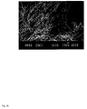
- Fig. 1a is a typical SEM image of Mo6S3I6 nanowires (the scale bar represents 10 µm);
- Fig. Ibis a typical SEM image of Mo4S3I3 nanowires (the scale bar represents 10 µm);
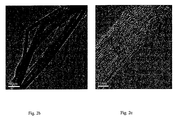
- Fig. 2a is a typical HRTEM image of Mo6S3I6 nanowire in the longitudinal direction (the scale bar represents 10 nm);
- Fig. 2b is a typical TEM image of Mo6S4.5I4.5 nanowire (the scale bar represents 50 nm);
- Fig. 2c is a typical TEM image of Mo6S4.5I4.5 nanowire (the scale bar represents 10 nm);
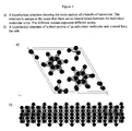
- Fig. 3a shows a hypothetical structure showing the cross-section of a bundle of nanowires.
- Fig. 3b shows a hypothetical structure of a short section of an individual molecular unit viewed from the side.
-
- The compounds in the present invention differ from the known materials described in the first section by their stoichiometry and/or their composition. The materials are stable in air and may be prepared in suspensions in polar fluids, such as water as well as non-polar organic liquids. It may be used in applications for field emission tips, as lubricants, in nanoelectronics and batteries, as sensor templates etc., and can be doped with other alkali ions or molecules, with a wide range of potential applications.
- According to a preferred embodiment the material M is a transition metal selected from the group consisting of Mo, W, V, Ti, Ta, Nb, Zn, Hf, Re and Ru.
- C may be any chalcogen but is preferably sulfur, selenium or tellurium. H may be any halogen, but is preferably Iodine or Bromide.
- According to another preferred embodiment 0<y<10 and 0≤z<10 while y+z>8.2. Also, in a specific embodiment, 8.2 < (y + z) < 10 and preferably y + z = 9.
- The invention relates to carbon nanotubes in that the form of growth and synthesis and preparation is such that it gives rise to similar appearance on the nanoscale. As is described by the terminology used in the field, the form of nanoropes, nanorods and nanowires.
- The invention relates to previous synthesis of M6C8-xTx, (M = transition metal, C = chalcogen, T = transition metal) and M6C8-xAx, (M = transition metal, C = chalcogen, A = alkali metal) all of which are synthesized below 1000 °C. The present invention differs from the compounds described in the previous statement by the synthesis being performed above 1000 °C, surprisingly yielding quasi-one dimensional objects in the form of nanoneedles, nanorods, nanowires or nanowhiskers.
- The present invention also relates to previously known forms of transition metal chalcogenide halides different stoichiometry, namely 662 stoichiometry, such as Mo6Se6I2 , which grow in the form of well-defined crystals. These materials have a well-defined crystal structure and also grow in the form of whiskers or rods. The present invention covers stoichiometries which differ from 662. The structural coherence is not present over distances more than 50 nm, arising from intrinsic reasons, such as bending or malleability of the material, which distinguishes the materials in this invention from crystalline whiskers or small crystals.
- The present invention relates to chain compounds with the formula MxCy such as Mo2S3 which have a different stoichiometry.
- The present invention relates to a MxCyHz material such as MoS2I1/3 which is grown in a modified transport reaction involving fullerenes such as C60 and C70. The present invention refers to material which differs from compounds such as MoS2I1/3 by the method of synthesis and by stoichiometry.
- The invention relates to items and devices, methods of making and using them and related systems on the scale of nanometers and micrometers.
- The present materials may be used in composites with enhanced mechanical, thermal or electrical properties, as battery electrodes, it may be with electrons or holes, as nanoconnectors, in nanodevices (e.g. FETs) in either metallic or semiconducting form depending on doping, connected to gold particles, as replacement material for carbon nanotubes, in applications which require one-dimensional structure or properties arising from confinement of electrons to one dimension, as field emission tips, as coatings, as catalyst, as superconductors, as carriers for functionalized sensors and detectors, as material utilising special chemical properties for attachment of various kinds of molecules or to surfaces, as solid-state lubricant and as additive material in liquid lubricants.
- In particular, the present materials may be embodied in a thin film or single rope, strand, needle, whisker or wire of said material deposited by evaporation of solvents, or electrodeposition including electrophoresis, dielectrophoresis etc. ,or in device made of single strands, multi-strand whiskers, ropes or rods of the Mo-S-I system, with items (i.e. atoms, molecules, contacts) attached either by van der Waals forces, via charge transfer or covalent bonding for purposes of functionalization and use for sensors, detectors, in which the specific chemical properties of the Mo-S-I materials are utilized, or as functionalised single strands, multi-strand whiskers, ropes or rods of the Mo-S-I system as in claim above in which a bond is made to the chalcogen (e.g.sulphur) or transition metal (e.g. molybdenum) or halogen (iodine).
- Said structures, which, when incorporated into devices using attached gold particles can form sensors, or on surfaces as films, used as an interface to temporary or permanent attachment of organic molecules via sulphur and/or carbon atom.
- In another embodiment, the invention is embodied as a conducting or superconducting wire, or rope or rod or whisker, composed of smaller wires, etc. which range in diameter from 0.2 nanometers to 10 micrometers.
- Said structures, which when dispersed into smaller bundles, ropes or individual tubes can act as lubricants, additives to lubricants, or components in composite materials in which friction can be reduced with or without the combination of increased strengths and/or enhanced electrical or thermal properties.
- In one aspect, the invention comprises the methods of growing, assembling and otherwise making articles and devices. In one embodiment a method of the invention involves growing rod-like, wire-like or rope-like objects composed of smaller quasi-one-dimensional subunits made of transition metal and chalcogen in various stoichiometry. In another embodiment, in addition to transition metal and chalcogen the objects may contain also other doped atoms or ions, or interstitial atoms, ions or molecules including halogens, other transition metals, rare-earth metals, organic donors etc.
- In one embodiment, the invention pertains to the synthesis of material under specific conditions above 1000 °C which has a particular shape of microrods, nanorods and nanowires, nanowhiskers, nanoropes, ranging in diameters from a few microns to a few nanometers. These microrods, nanorods and nanowires are typically composite objects, composed of thin one-dimensional objects such as wires, strings or clusters of atoms arranged in straight or staggered chains or ladders.
- In another embodiment the invention is described as material whose wire-like or rod-like shape concentrates electric fields at their tips.
- In another embodiment the invention is described as a conducing nanowire, nanorope, nanorod, etc. of intertwined strands of smaller wires, strands ranging in diameter from 0.4 nm to 10000 nm.
- The following examples illustrate the invention without limiting it thereto.
- The synthesis is performed in a sealed and evacuated quartz ampoule having diameter of 19 mm and a length of 140 mm, (remaining gas pressure < 10-3 torr) containing platelets of Mo sheet metal (Aldrich, molybdenum foil 0.1 mm thick, 99.9+%), S (Aldrich, sulfur powder, 99.98 %) and I2 (Aldrich, 99.999+%) in the amounts 6:4:6 (Mo: 0.8925 g, S: 0.1988 g, I2: 1.1805 g). The ampoule is placed in a single-zone furnace ( LINDBERG STF 55346C) and heated from room temperature to a temperature of 1070 °C at a rate 8 K per hour. This temperature is kept stable for 72 hours. The ampoule is then cooled at 1,5 K per minute. The resulting material contains a large amount of material in the form of furry-like material (Figure 2), which upon closer examination contains ropes of material with stoichiometry given by Mo6S3I6.
- The composition, as determined by EA (elemental analysis) is given as Mo6S3I6.
found, %: Mo 40,4; S 6,4; I 53,1. (measurement tolerance ± 0,2 - 0,3 %)
calculated for Mo6S3I6, % : Mo 40,2; S 6,7; I 53,1.
The chemical composition corresponds to the molar ratio Mo : S : I = 2 : 1 : 2. - The structure of the material as grown is essentially crystalline in the usual sense. X-ray data shown rather broad peaks with no narrow well-defined sharp crystal peaks.
- The synthesis is performed in sealed and evacuated quartz ampoule (diameter 19 mm, length 140 mm), (remaining gas pressure < 10-3 torr) containing platelets of Mo sheet metal (Aldrich, molybdenum foil 0.1 mm thick, 99.9+%), S (Aldrich, sulfur powder, 99.98 %) and I2 (Aldrich, 99.999+%) in the amounts 6:4:4 (Mo: 0.8981 g, S: 0.2000 g, I2: 0.7919 g). The ampoule is placed in a single-zone furnace (LINDBERG STF 55346C) and heated from room temperature to a temperature of 1150 °C at a rate 8 K per hour. This temperature is kept stable for 72 hours. The ampoule is then cooled at 1,5 K per minute. The resulting material contains a large amount of material in the form of furry-like material (Figure 2), which upon closer examination contains ropes of material with stoichiometry given by Mo6S4.5I4.5.
- The composition, as determined EA (elemental analysis) is given as Mo6S4.5I4.5.
found % Mo 43,5; S 11,2; I 45,3 (measure tolerance ± 0,3%) calculated for Mo6S4.5I4.5, % Mo 44,6; S 11,2; I 44,2. - The structure of the material as grown is not crystalline in the usual sense, particularly along the direction of the wires, because of the very weak forces in-between the wires. X-ray data shown rather broad peaks with no narrow well-defined sharp crystal peaks, particularly in the direction along the wires.
- The microscopic structure cannot be described in terms of rolled-up sheets of layered dichalcogenide material, and cannot be described to be fullerene-like in structure.
- The morphology of the material is in the form of needles or ropes or wires, composed of small-diameter columnar structures.
- The material can be dispersed in a variety of solvents, such as isopropanol, methanol, water etc., using an ultrasonic bath, to various degrees, where the mean diameter of the nanowires thus obtained depends on the dilution and on the extent of sonification. Thinner diameters are obtained with more dilute solutions, and monodisperse dispersions of nanowires with mean diameter less than 4 nm can be obtained using this method with dilutions.
- The materials are grown at temperatures above 1000 °C. Their stoichiometry is variable, and different compounds exist, which have different values y and z.
Claims (14)
- A material of the general formula M6C y H z , wherein M designates a transition metal, C designates a chalcogen, H designates a halogen, and wherein y and z may be of from 0 to 10 such that 8.2<y+z<10, grown in the form of nanowires, nano-ropes, nanorods, whiskers or needles and obtainable by a process comprising the steps of mixing the constituent elements in the desired mass ratio, placing them in an appropriate container, evacuating the container and heating it to a temperature above 1000 °C for a predetermined length of time.
- The material according to claim 1, wherein M is a transition metal selected from the group consisting of Mo, W, V, Ti, Ta, Nb, Zn, Hf, Re and Ru.
- The material according to claim 1 or 2, wherein C = S, Se, Te.
- The material according any of the preceding claims, wherein the halogen H= I, Br.
- The material according to any of the preceding claims, wherein 0<y<10, 0<z<10 and 8.2≤y+z<10.
- The material according to any of the preceding claims, wherein H may be replaced by an ion elected from the group consisting of elements in the groups III-VIII.
- The material according to any of the preceding claims, additionally containing intercalated or interstitial ions, atoms or molecules, selected from the group consisting of alkali metals, alkaline-earth metals, transition metals, elements belonging ro groups III-VIII and any organic donors or acceptors..
- The material according to any of the preceding claims exhibiting a substantially circular cross-section.
- The material according to any of the preceding claims, which is superconducting.
- The material according to any of the preceding claims, which is metallic or semiconducting.
- A method for the production of a material according to any of the claims 1 to 11, which comprises the steps of (i) mixing of the individual constituent elements, (ii) heating in a sealed container under reduced pressure, (iii) heating above a temperature of 1000 C or more for any duration of time.
- The method according to claim 11, wherein the elements themselves are replaced by compounds of those elements such as MoS2 for example.
- Use of a material according to any of the preceding claims in electronic, chemical, optical or mechanical applications.
- Use of a material according to any of the claims 1 to 12 as a catalyst in dry form or in suspension or as a catalytic component.
Priority Applications (8)
| Application Number | Priority Date | Filing Date | Title |
|---|---|---|---|
| EP03028188A EP1541528A1 (en) | 2003-12-08 | 2003-12-08 | Quasi-one-dimensional polymers based on the metal-chalcogen-halogen system |
| CNA2004800365560A CN1890182A (en) | 2003-12-08 | 2004-02-25 | Quasi-one-dimensional polymers based on the metal-chalcogen-halogen system |
| PCT/EP2004/001870 WO2005058758A1 (en) | 2003-12-08 | 2004-02-25 | Quasi-one-dimensional polymers based on the metal-chalcogen-halogen system |
| CA002548265A CA2548265A1 (en) | 2003-12-08 | 2004-02-25 | Quasi-one-dimensional polymers based on the metal-chalcogen-halogen system |
| JP2006543371A JP2007513050A (en) | 2003-12-08 | 2004-02-25 | Quasi-one-dimensional polymer based on metal-chalcogen-halogen system |
| KR1020067013415A KR20060123431A (en) | 2003-12-08 | 2004-02-25 | Metal-chalcogen-halogen based semi-dimensional polymers |
| US10/582,173 US20070274895A1 (en) | 2003-12-08 | 2004-02-25 | Quasi-One-Dimensional Polymers Based on the Metal-Chalcogen-Halogen System |
| IL176211A IL176211A0 (en) | 2003-12-08 | 2006-06-08 | Quasi-one-dimensional-polymers based on the metal-chalcogen-halogen system |
Applications Claiming Priority (1)
| Application Number | Priority Date | Filing Date | Title |
|---|---|---|---|
| EP03028188A EP1541528A1 (en) | 2003-12-08 | 2003-12-08 | Quasi-one-dimensional polymers based on the metal-chalcogen-halogen system |
Publications (1)
| Publication Number | Publication Date |
|---|---|
| EP1541528A1 true EP1541528A1 (en) | 2005-06-15 |
Family
ID=34486143
Family Applications (1)
| Application Number | Title | Priority Date | Filing Date |
|---|---|---|---|
| EP03028188A Withdrawn EP1541528A1 (en) | 2003-12-08 | 2003-12-08 | Quasi-one-dimensional polymers based on the metal-chalcogen-halogen system |
Country Status (8)
| Country | Link |
|---|---|
| US (1) | US20070274895A1 (en) |
| EP (1) | EP1541528A1 (en) |
| JP (1) | JP2007513050A (en) |
| KR (1) | KR20060123431A (en) |
| CN (1) | CN1890182A (en) |
| CA (1) | CA2548265A1 (en) |
| IL (1) | IL176211A0 (en) |
| WO (1) | WO2005058758A1 (en) |
Cited By (1)
| Publication number | Priority date | Publication date | Assignee | Title |
|---|---|---|---|---|
| WO2008121081A2 (en) | 2007-03-30 | 2008-10-09 | Institut 'jozef Stefan' | A process for the synthesis of nanotubes and fullerene-like nanostructures of transition metals dichalcogenides, quasi one-dimensional structures of transition metals and oxides of transition metals |
Families Citing this family (18)
| Publication number | Priority date | Publication date | Assignee | Title |
|---|---|---|---|---|
| US7442575B2 (en) * | 2006-09-29 | 2008-10-28 | Texas Christian University | Method of manufacturing semiconductor nanowires |
| TWI556456B (en) | 2007-04-20 | 2016-11-01 | 坎畢歐科技公司 | Composite transparent conductor and method of forming same |
| KR101251538B1 (en) | 2009-04-17 | 2013-04-08 | (주)아벨리노 | Primer for Avellino Corneal Dystrophy |
| KR101041606B1 (en) * | 2009-08-18 | 2011-06-15 | (주)아벨리노 | Nucleic acid chip for diagnosing corneal dysfunction with multi-spot metal-deposited nanostructure array and its manufacturing method |
| US8865402B2 (en) * | 2009-08-26 | 2014-10-21 | Clemson University Research Foundation | Nanostructured substrates for surface enhanced raman spectroscopy (SERS) and detection of biological and chemical analytes by electrical double layer (EDL) capacitance |
| TWI420540B (en) * | 2009-09-14 | 2013-12-21 | Ind Tech Res Inst | Conductive material formed by light energy or thermal energy, preparation method of conductive material, and conductive composition |
| WO2012108853A1 (en) * | 2009-12-04 | 2012-08-16 | Cambrios Technologies Corporation | Nanostructure-based transparent conductors having increased haze and devices comprising the same |
| KR101125212B1 (en) | 2010-10-01 | 2012-03-21 | (주)아벨리노 | System for diagnosis of avellino corneal dystrophy |
| WO2013148211A1 (en) | 2012-03-30 | 2013-10-03 | The Trustees Of Columbia University In The City Of New York | Solid-state materials formed of molecular clusters and method of forming same |
| US10889850B2 (en) | 2013-03-15 | 2021-01-12 | Avellino Lab Usa, Inc. | Methods for improved isolation of genomic DNA templates for allele detection |
| EP2925895B1 (en) | 2013-03-15 | 2018-11-28 | Avellino Lab USA, Inc. | Methods for improved isolation of genomic dna templates for allele detection |
| AU2014348279B2 (en) | 2013-11-15 | 2021-02-18 | Avellino Lab Usa, Inc. | Methods for multiplex detection of alleles associated with ophthalmic conditions |
| KR20160084715A (en) * | 2015-01-06 | 2016-07-14 | 연세대학교 산학협력단 | Transparent electrode and manufacturing method thereof |
| KR101830198B1 (en) | 2015-06-25 | 2018-02-20 | 고려대학교 산학협력단 | Biomolecule-polymer nanofiber composite and Preparing method thereof |
| WO2017083852A1 (en) | 2015-11-13 | 2017-05-18 | MOORE, Tara | Methods for the treatment of corneal dystrophies |
| IL249804A0 (en) | 2016-12-27 | 2017-04-02 | Yeda Res & Dev | Electromechanical devices based on metal-chalcogenide nanotubes |
| KR102075443B1 (en) * | 2019-07-03 | 2020-02-10 | 성균관대학교산학협력단 | Hydrogel composite and preparing method thereof |
| CN114769581B (en) * | 2022-04-29 | 2023-09-05 | 西安交通大学 | Transition metal sulfide nano onion, preparation method and application thereof |
Citations (3)
| Publication number | Priority date | Publication date | Assignee | Title |
|---|---|---|---|---|
| US5958358A (en) | 1992-07-08 | 1999-09-28 | Yeda Research And Development Co., Ltd. | Oriented polycrystalline thin films of transition metal chalcogenides |
| US6217843B1 (en) | 1996-11-29 | 2001-04-17 | Yeda Research And Development Co., Ltd. | Method for preparation of metal intercalated fullerene-like metal chalcogenides |
| WO2004013884A1 (en) * | 2002-08-02 | 2004-02-12 | Institut 'josef Stefan' | Use of quasi-one-dimensional transition metal ternary compounds and quasi-one-dimensional transition metal chalcogenide compounds as electron emitters |
Family Cites Families (1)
| Publication number | Priority date | Publication date | Assignee | Title |
|---|---|---|---|---|
| GB0210041D0 (en) * | 2002-05-02 | 2002-06-12 | Univ Durham | "High-field superconductors" |
-
2003
- 2003-12-08 EP EP03028188A patent/EP1541528A1/en not_active Withdrawn
-
2004
- 2004-02-25 CA CA002548265A patent/CA2548265A1/en not_active Abandoned
- 2004-02-25 US US10/582,173 patent/US20070274895A1/en not_active Abandoned
- 2004-02-25 KR KR1020067013415A patent/KR20060123431A/en not_active Withdrawn
- 2004-02-25 JP JP2006543371A patent/JP2007513050A/en active Pending
- 2004-02-25 WO PCT/EP2004/001870 patent/WO2005058758A1/en not_active Ceased
- 2004-02-25 CN CNA2004800365560A patent/CN1890182A/en active Pending
-
2006
- 2006-06-08 IL IL176211A patent/IL176211A0/en unknown
Patent Citations (3)
| Publication number | Priority date | Publication date | Assignee | Title |
|---|---|---|---|---|
| US5958358A (en) | 1992-07-08 | 1999-09-28 | Yeda Research And Development Co., Ltd. | Oriented polycrystalline thin films of transition metal chalcogenides |
| US6217843B1 (en) | 1996-11-29 | 2001-04-17 | Yeda Research And Development Co., Ltd. | Method for preparation of metal intercalated fullerene-like metal chalcogenides |
| WO2004013884A1 (en) * | 2002-08-02 | 2004-02-12 | Institut 'josef Stefan' | Use of quasi-one-dimensional transition metal ternary compounds and quasi-one-dimensional transition metal chalcogenide compounds as electron emitters |
Non-Patent Citations (4)
| Title |
|---|
| DATABASE CA [online] CHEMICAL ABSTRACTS SERVICE, COLUMBUS, OHIO, US; 12 May 1984 (1984-05-12), C. PERRIN, M. POTEL, M. SERGENT: "Molybdenum bromide sulfide (Mo6Br6S3) : a new two-dimensional compound with octahedral Mo6-Clusters", XP002283921, Database accession no. 98:170737 * |
| DATABASE CA [online] CHEMICAL ABSTRACTS SERVICE, COLUMBUS, OHIO, US; 12 May 1984 (1984-05-12), C. PERRIN, M. SERGENT, J.C. PILET, F. LE TRAON, A. LE TRAON: "Structure-property relations in new Mo(III) and Mo(II) chalcohalogenides with Mo4 and Mo6 clusters", XP002283920, Database accession no. 99:46283 * |
| M. REMSKAR, . MRZEL, R. SANJINES, H. COHEN, F. LÉVY: "Metallic Sub-Nanometer MoS(2-x)I(y) Nanotubes", ADVANCED MATERIAL, vol. 15, no. 3, 2003, pages 237 - 240, XP002283919 * |
| RAMSKAR M ET AL: "SELF-ASSEMBLY OF SUBNANOMETER-DIAMETER SINGLE-WALL MOS2 NANOTUBES", SCIENCE, AMERICAN ASSOCIATION FOR THE ADVANCEMENT OF SCIENCE,, US, vol. 292, no. 5516, 20 April 2001 (2001-04-20), pages 479 - 481, XP001156527, ISSN: 0036-8075 * |
Cited By (1)
| Publication number | Priority date | Publication date | Assignee | Title |
|---|---|---|---|---|
| WO2008121081A2 (en) | 2007-03-30 | 2008-10-09 | Institut 'jozef Stefan' | A process for the synthesis of nanotubes and fullerene-like nanostructures of transition metals dichalcogenides, quasi one-dimensional structures of transition metals and oxides of transition metals |
Also Published As
| Publication number | Publication date |
|---|---|
| JP2007513050A (en) | 2007-05-24 |
| WO2005058758A1 (en) | 2005-06-30 |
| IL176211A0 (en) | 2006-10-05 |
| US20070274895A1 (en) | 2007-11-29 |
| KR20060123431A (en) | 2006-12-01 |
| CA2548265A1 (en) | 2005-06-30 |
| CN1890182A (en) | 2007-01-03 |
Similar Documents
| Publication | Publication Date | Title |
|---|---|---|
| Serra et al. | An overview of the recent advances in inorganic nanotubes | |
| Tenne | Inorganic nanotubes and fullerene-like nanoparticles | |
| Kim et al. | Zinc oxide nanowires on carbon nanotubes | |
| Tenne et al. | Inorganic nanotubes | |
| Rao et al. | Inorganic nanotubes | |
| Rao et al. | Synthesis of inorganic nanotubes | |
| Xiong et al. | Some recent developments in the chemical synthesis of inorganic nanotubes | |
| Li et al. | Single‐crystalline In2O3 nanotubes filled with In | |
| Hu et al. | Ultrathin nanostructures: smaller size with new phenomena | |
| Banerjee et al. | Large-quantity free-standing ZnO nanowires | |
| Tenne et al. | Nanotubes from inorganic materials | |
| US20070274895A1 (en) | Quasi-One-Dimensional Polymers Based on the Metal-Chalcogen-Halogen System | |
| Tenne et al. | Inorganic nanotubes and fullerene-like structures (IF) | |
| Tian et al. | Synthesis and growth mechanism of various SiO2 nanostructures from straight to helical morphologies | |
| Bera | Synthesis, properties and applications of amorphous carbon nanotube and MoS2 Nanosheets: a review | |
| Jin et al. | Catalysed growth of novel aluminium oxide nanorods | |
| Zhu et al. | Co-catalysed VLS growth of novel ceramic nanostructures | |
| Shen et al. | One-step construction of ZnS/C and CdS/C one-dimensional core–shell nanostructures | |
| Bera et al. | A detail opto-electronic and photocatalytic study of amorphous carbon nanotubes—MoS2 hybrids | |
| CN1753835A (en) | Nanostructures | |
| WO2007051481A2 (en) | Use of quasi-one-dimensional polymers based on the metal-chalcogen-halogen system | |
| Rao et al. | Multiwalled HgX (X= S, Se, Te) Nanotubes Formed with a Mercury Iodide Catalyst in Nanocrystalline Thin Films Spray‐Deposited at Low Temperature | |
| Hu et al. | Morphological evolution of Nb2O5 in a solvothermal reaction: From Nb2O5 grains to Nb2O5 nanorods and hexagonal Nb2O5 nanoplatelets | |
| Xu et al. | CVD of nanowires and nanotubes, mass production, and industrialization | |
| Ye et al. | Synthesis and the field emission performances of SnO2 micrograsses |
Legal Events
| Date | Code | Title | Description |
|---|---|---|---|
| PUAI | Public reference made under article 153(3) epc to a published international application that has entered the european phase |
Free format text: ORIGINAL CODE: 0009012 |
|
| AK | Designated contracting states |
Kind code of ref document: A1 Designated state(s): AT BE BG CH CY CZ DE DK EE ES FI FR GB GR HU IE IT LI LU MC NL PT RO SE SI SK TR |
|
| AX | Request for extension of the european patent |
Extension state: AL LT LV MK |
|
| 17P | Request for examination filed |
Effective date: 20051208 |
|
| AKX | Designation fees paid |
Designated state(s): AT BE BG CH CY CZ DE DK EE ES FI FR GB GR HU IE IT LI LU MC NL PT RO SE SI SK TR |
|
| 17Q | First examination report despatched |
Effective date: 20060818 |
|
| STAA | Information on the status of an ep patent application or granted ep patent |
Free format text: STATUS: THE APPLICATION IS DEEMED TO BE WITHDRAWN |
|
| 18D | Application deemed to be withdrawn |
Effective date: 20090701 |