EP1538746A2 - Balun device - Google Patents
Balun device Download PDFInfo
- Publication number
- EP1538746A2 EP1538746A2 EP04257516A EP04257516A EP1538746A2 EP 1538746 A2 EP1538746 A2 EP 1538746A2 EP 04257516 A EP04257516 A EP 04257516A EP 04257516 A EP04257516 A EP 04257516A EP 1538746 A2 EP1538746 A2 EP 1538746A2
- Authority
- EP
- European Patent Office
- Prior art keywords
- balun
- matching circuit
- line
- unbalanced
- band side
- Prior art date
- Legal status (The legal status is an assumption and is not a legal conclusion. Google has not performed a legal analysis and makes no representation as to the accuracy of the status listed.)
- Withdrawn
Links
Images






Classifications
-
- H—ELECTRICITY
- H03—ELECTRONIC CIRCUITRY
- H03H—IMPEDANCE NETWORKS, e.g. RESONANT CIRCUITS; RESONATORS
- H03H7/00—Multiple-port networks comprising only passive electrical elements as network components
- H03H7/42—Networks for transforming balanced signals into unbalanced signals and vice versa, e.g. baluns
Definitions
- the present invention relates to a balun (balanced-to-unbalanced transformer) that connects a balanced circuit and an unbalanced circuit together, for example, for transforming the impedance of transmission lines in a high frequency of UHF band or higher.
- a balun balanced-to-unbalanced transformer
- JP-A-2002-43882 As a conventional balun, a technique disclosed in JP-A-2002-43882 is known. In the balun disclosed in this document, a band-pass filter is connected to the terminal of an unbalanced line of the balun. As an alternative example, a technique disclosed in JP-A-2002-271036 is known. The circuit of this technique is provided, as shown in Fig.
- balun 20 which is composed of an unbalanced transmission line 25 and a pair of balanced transmission lines 26
- second-order low-pass filter 27 which is composed of an inductor (L) and a capacitor (C) connected to the unbalanced transmission line
- a matching circuit 22 of diplexer which is composed of a third-order high-pass filter 28 that is composed of an L and three Cs.
- ultra wide band communication equipment e.g. mobile phone and wireless LAN
- its standard desires that such equipment transmits an ultra wide band of about 3GHz to 10GHz with a flat characteristic.
- the band must be made broader than that used before. It causes another problem, however, that such a filter or balun tends to become larger in size if the ultra wide band is designed by a commonly known method. Therefore, it is unsuitable as a device expected to be built in equipment, such as mobile phones, that are required to be microminiaturized.
- the present invention is intended to solve at least one of the above problems, and accordingly, an object of the invention is to provide a balun in which the ultra wide band can be realized and the size can be miniaturized.
- the balun according to the present invention has been directed to achieve the above object, and the first aspect of the invention comprises a balun unit, which is provided with a balanced line and an unbalanced line, and a matching circuit connected to the unbalanced line, wherein the matching circuit is composed of a high-pass filter.
- the second aspect of the invention is configured similarly to the first aspect, wherein the high-pass filter comprises a capacitor connected in series to the unbalanced line and an inductor connected in parallel to the unbalanced line, and wherein the capacitor is connected at a side closer to the balun unit than the inductor is.
- the third aspect of the invention comprises a balun unit provided with a balanced line and an unbalanced line, and a matching circuit connected to the unbalanced line, wherein length of a strip line in the balun unit is made shorter than a fundamental length ⁇ /4 to shift a center frequency to a higher band side, and the shifted portion is compensated with an expansion to a lower band side by inserting the matching circuit, so that the balun device as a whole has an ultra wide band and is miniaturized.
- the fourth aspect of the invention comprises a balun unit provided with a balanced line and an unbalanced line, and a matching circuit connected to the unbalanced line, wherein the balun unit is composed of a capacitor and an inductor element that give a resonant frequency lower than a resonant frequency coincided with an applied center frequency, to shift a center frequency to a higher band side, and the shifted portion is compensated with an expansion to a lower band side by inserting the matching circuit, so that the balun device as a whole has an ultra wide band and is miniaturized.
- the fifth aspect of the invention comprises a balun unit provided with a balanced line and an unbalanced line, and a matching circuit connected to the unbalanced line, wherein the matching circuit has an improved reflective property compared to the balun unit, in vicinity of cut-off frequency at a lower band side of a used band.
- the sixth aspect of the invention comprises a balun unit provided with a balanced line and an unbalanced line, and a matching circuit connected to the balanced line, wherein the length of a strip line in the balun unit is made shorter than a fundamental length ⁇ /4 to shift a center frequency to a higher band side, and the shifted portion is compensated with an expansion to lower band side by inserting the matching circuit, so that the balun device as a whole has an ultra wide band and is miniaturized.
- the seventh aspect of the invention comprises a balun unit provided with a balanced line and an unbalanced line, and a matching circuit connected to the balanced line, wherein the balun unit is composed of a capacitor and an inductor element that give a resonant frequency lower than a resonant frequency coincided with an applied center frequency, to shift a center frequency to a higher band side, and the shifted portion is compensated with an expansion to a lower band side by inserting the matching circuit, so that the balun device as a whole has an ultra wide band and is miniaturized.
- the eighth aspect of the invention comprises a balun unit provided with a balanced line and an unbalanced line, and a matching circuit connected to the balanced line, wherein the matching circuit has an improved reflective property compared to the balun unit, in vicinity of cut-off frequency at a lower band side of a used band.
- the matching circuit connected to the unbalanced line of the balun is composed of a high-pass filter
- the lower band is expanded and the balun device can perform the ultra-wide band characteristic.
- the high-pass filter comprises a capacitor connected in series to the unbalanced line and an inductor connected in parallel to the unbalanced line, wherein the capacitor is connected at a side closer to the balun unit than the inductor is, the frequency characteristic at a lower band is improved.
- the balun can perform the ultra-wide band characteristic and be miniaturized.
- the term "used band” means the frequency band that is used in the communication equipment into which the balun according to the present invention is built, for example, the frequency band is 3GHz to 10GHz as mentioned above, and in that case, the "cut-off frequency at a lower band side" is 3GHz.
- the balun device as a whole has an ultra wide band and the size of the balun itself can be miniaturized.
- the present invention comprises a balun unit provided with a balanced line and an unbalanced line, and a matching circuit connected to the balanced line, wherein the length of a strip line in the balun unit is made shorter than a fundamental length ⁇ /4 to shift a center frequency to a higher band side, and the shifted portion is compensated with an expansion to a lower band side by inserting the matching circuit, so that the balun device as a whole has an ultra wide band and is miniaturized.
- Example 1 of balun according to the present invention will be described below referring to Figs. 1-5.
- Fig. 1 is a circuit diagram of the balun showing Example 1, in which the unit numbered 1 shows a balun unit having an unbalanced line 11 and two balanced lines 12, 13, and the unit numbered 2 shows a matching circuit in the form of a high-pass filter, which is composed of a capacitor C1 connected to the unbalanced line and an inductor L1, the capacitor C1 in the matching circuit 2 being connected in series to the unbalanced line 11 and the inductor L1 being connected in parallel to the unbalanced line 11 through the capacitor C1.
- a high-pass filter which is composed of a capacitor C1 connected to the unbalanced line and an inductor L1, the capacitor C1 in the matching circuit 2 being connected in series to the unbalanced line 11 and the inductor L1 being connected in parallel to the unbalanced line 11 through the capacitor C1.
- the length of a strip line in the balun unit is made shorter than ⁇ /4 of the applied center frequency (the center frequency defined in the communications standard), while, when the balun unit 1 is composed of an LC element the LC circuit is configured so as to give a smaller value than the LC value generating the center frequency coincided with the applied center frequency (See Fig. 2).
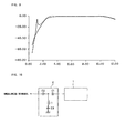
- the capacitor C1 is connected in series to the balun unit 1 and the inductor L1 is connected in parallel to the unbalanced line 11 via the capacitor C1 so that the lower band side is expanded as shown in Fig. 3.
- the portion of the center frequency shifted to a higher band side is compensated by the matching circuit 2 composed of a high-pass filter, and it as a whole enables the balun device to provide an ultra wide band.
- the high-pass filter composing a matching circuit 2 in which the capacitor C1 is connected in series to the balun unit 1, and the inductor L1 is connected in parallel to the unbalanced line 11 through the capacitor C1, as in the present invention, a better reflection loss is obtained than in the case of the balun alone, in vicinity of the cut-off frequency at a lower band side as shown in Fig. 5, i.e. the lower band side is improved.
- the dotted line indicates the reflection loss of the balun alone; the two-dot chain line indicates the reflection loss of the high-pass filter; and the solid line indicates the combined reflection loss thereof.
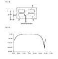
- the matching circuit 2 is composed of two capacitors C1, C2, which are connected in series to the unbalanced line 11 as shown in Fig. 6, and an inductor L1 which is connected to the joining point between the two capacitors C1, C2, and it provides the improved ultra wide band characteristic that is nearly the same as in the above-described Example 1 (See Fig. 7).
- dotted line indicates the property without the matching circuit 2; and solid line indicates the property with the matching circuit 2 connected. The same indication will be used hereinafter.
- the matching circuit 2 is composed of a capacitor C1 which is connected in series to the unbalanced line 11 as shown in Fig. 8, and two inductors L1, L2 which are connected to both ends of the capacitor C1. Although the result shows an abnormal waveform partially at lower frequency, its ultra wide band is still secured (See Fig. 9).
- Example 4 the matching circuit 2 is the same as that of Example 2 except that a capacitor C3 is inserted in series between the inductor L1 and the ground. Differently from the result of Example 2, obtained characteristic of an ultra wide band is flat even at the lower frequency (See Fig. 11).
- the matching circuit 2 is composed of only a capacitor C1 connected to the unbalanced line 11. Since the capacitor C1 shows a low impedance at a high frequency, it gives the same waveform as that of the case without a matching circuit (indicated by a dashed line) as shown in Fig. 13, therefore it means nothing but a mere wiring and does not have an advantage of connecting the capacitor.
- the matching circuit 2 is composed of only an inductor L1 connected to the unbalanced line 11. Since the inductor L1 shows a high impedance information, producing a state where the inductor L1 is disconnected, it gives substantially the same waveform as that of the case without a matching circuit (indicated by a dashed line) as shown in Fig. 15, therefore it does not have an advantage as a matching circuit.
- the matching circuit 2 is composed of a capacitor C1 which is connected in series to the unbalanced line 11, and an inductor L1 which is connected in parallel close to the balun unit 1.
- a dash line the waveform of the case without a matching circuit (indicated by a dash line)
- it gives a waveform that descends at a lower band side and then raises only slightly its level, as shown in Fig. 17, therefore it does not have an advantage as a matching circuit.
- the matching circuit 2 is composed of a capacitor C1 and an inductor L1 connected together in parallel, and is connected to the unbalanced line 11. It gives the same waveform as that of the case without a matching circuit (indicated by a dashed line) as shown in Fig. 19, therefore it does not have an advantage as a matching circuit.
- the matching circuit 2 in this Example 5 is configured as a high-pass filter composed of two capacitors C1, C2 which are connected in series to respective input/output terminals of balanced signals in the balanced lines 12, 13, and two inductors L1, L2 which are inserted between respective capacitors C1, C2 and the ground, as shown in Fig. 20A.
- Fig. 20A is the matching circuit 2 that is a high-pass filter
- Fig. 20B is the matching circuit in which two capacitors C1, C2 are connected to respective input/output terminals for balanced outputs.
- circuit 2 enables the resonator to be shorter than ⁇ /4, while in the case of the LC type, a smaller LC constant can be selected. Consequently, the property in which the center frequency is shifted to the higher band side and the lower band side is expanded can be obtained, similarly to the curve shown in Fig. 4.
- the properties of those examples are improved in the expansion of transmitting band and the reflective property at the lower band side, and, since the resonator can be made shorter at the higher band side, the properties are also improved in the expansion at the higher frequency band, compared with the properties of the conventional balun (indicated by one-dot and two-dot chain lines). Consequently, it is possible as a whole to design with a higher resonant point, taking an advantage of the expansion of transmitting band and that at lower band. As the result, the resonator can be made shorter, therefore the balun device can be miniaturized.
Landscapes
- Control Of Motors That Do Not Use Commutators (AREA)
- Filters And Equalizers (AREA)
- Coils Or Transformers For Communication (AREA)
- Networks Using Active Elements (AREA)
Abstract
Description
Claims (8)
- A balun device comprising a balun portion unit provided with a balanced line and an unbalanced line, and a matching circuit connected to the unbalanced line,
wherein the matching circuit is composed of a high-pass filter. - The balun device as claimed in Claim 1, wherein the high-pass filter comprises a capacitor connected in series to the unbalanced line and an inductor connected in parallel to the unbalanced line, and wherein the capacitor is connected at a side closer to the balun portion than the inductor.
- A balun device comprising a balun portion provided with a balanced line and an unbalanced line, and a matching circuit connected to the unbalanced line,
wherein length of a strip line in the balun portion is shorter than a fundamental length of λ/4 to shift a center frequency to higher band side, and shiftedportion is compensated with an expansion to lower band side by inserting the matching circuit, so that the balun device has an ultra wide band characteristic and is miniaturized. - A balun device comprising a balun portion provided with a balanced line and an unbalanced line, and a matching circuit connected to the unbalanced line,
wherein the balun unit is composed of a capacitor and an inductor elements that give a resonant frequency lower than a resonant frequency coincided with an applied center frequency, to shift a center frequency to higher band side, and shifted portion is compensated with an expansion to lower band side by inserting the matching circuit, so that the balun device has an ultra wide band characteristic and is miniaturized. - A balun device comprising a balun portion provided with a balanced line and an unbalanced line, and a matching circuit connected to the unbalanced line,
wherein the matching circuit has an improved reflective property compared to that of the balun portion, in vicinity of cut-off frequency at a lower band side. - A balun device comprising a balun portion , which is provided with a balanced line and an unbalanced line, and a matching circuit connected to the balanced line,
wherein length of a strip line in the balun portion is shorter than λ/4 which is a fundamental length, to shift a center frequency to higher band side, and shifted portion is compensated with an expansion to lower band side by inserting the matching circuit, so that the balun device has an ultra wide band characteristic and is miniaturized. - A balun device comprising a balun portion provided with a balanced line and an unbalanced line, and a matching circuit connected to the balanced line,
wherein the balun unit is composed of a capacitor and an inductor element that give a resonant frequency lower than a resonant frequency coincided with an applied center frequency, to shift a center frequency to higher band side, and shifted portion is compensated with an expansion to lower band side by inserting the matching circuit, so that the balun device has an ultra wide band characteristic and is miniaturized. - A balun device comprising a balun portion provided with a balanced line and an unbalanced line, and a matching circuit connected to the balanced line,
wherein the matching circuit has an improved reflective property compared to that of the balun portion, in vicinity of cut-off frequency at a lower band side.
Applications Claiming Priority (4)
| Application Number | Priority Date | Filing Date | Title |
|---|---|---|---|
| JP2003407680 | 2003-12-05 | ||
| JP2003407680 | 2003-12-05 | ||
| JP2004277894A JP4042860B2 (en) | 2003-12-05 | 2004-09-24 | Balun |
| JP2004277894 | 2004-09-24 |
Publications (2)
| Publication Number | Publication Date |
|---|---|
| EP1538746A2 true EP1538746A2 (en) | 2005-06-08 |
| EP1538746A3 EP1538746A3 (en) | 2007-11-07 |
Family
ID=34467864
Family Applications (1)
| Application Number | Title | Priority Date | Filing Date |
|---|---|---|---|
| EP04257516A Withdrawn EP1538746A3 (en) | 2003-12-05 | 2004-12-03 | Balun device |
Country Status (4)
| Country | Link |
|---|---|
| US (1) | US7205861B2 (en) |
| EP (1) | EP1538746A3 (en) |
| JP (1) | JP4042860B2 (en) |
| CN (1) | CN1625045A (en) |
Cited By (3)
| Publication number | Priority date | Publication date | Assignee | Title |
|---|---|---|---|---|
| EP1949490A4 (en) * | 2005-09-14 | 2011-12-07 | Bae Sys Inf & Elect Sys Integ | Broadband transmission line transformer |
| CN109962324A (en) * | 2019-03-29 | 2019-07-02 | 哈尔滨工业大学 | Miniaturized and compact duplexer based on thin film integrated passive device process |
| SE2100010A1 (en) * | 2021-01-21 | 2022-07-22 | Saab Ab | Compact balun with out-of-band spurious suppression |
Families Citing this family (14)
| Publication number | Priority date | Publication date | Assignee | Title |
|---|---|---|---|---|
| CN1983712B (en) * | 2005-12-16 | 2010-05-19 | 财团法人工业技术研究院 | Balance to unbalance converter with filter function |
| JP2007189396A (en) * | 2006-01-12 | 2007-07-26 | Seiko Epson Corp | Balun |
| CN101488598B (en) * | 2006-03-25 | 2013-01-09 | 鸿富锦精密工业(深圳)有限公司 | Balance to unbalance converter |
| JP5131495B2 (en) * | 2010-07-29 | 2013-01-30 | Tdk株式会社 | Thin film balun |
| JP5522130B2 (en) | 2011-08-01 | 2014-06-18 | 株式会社村田製作所 | Unbalance-balance conversion circuit element |
| US8669829B2 (en) * | 2012-02-27 | 2014-03-11 | Teledyne Wireless, Llc | Multi-octave power amplifier |
| TWI513184B (en) * | 2012-07-11 | 2015-12-11 | 矽品精密工業股份有限公司 | Balanced to unbalanced converter |
| TWI545893B (en) | 2014-04-07 | 2016-08-11 | 國立臺灣科技大學 | Balun device |
| TW201628254A (en) * | 2015-01-26 | 2016-08-01 | Trans Electric Co Ltd | Balance/unbalance converter |
| JP6511962B2 (en) * | 2015-05-28 | 2019-05-15 | Tdk株式会社 | Stacked electronic components |
| JP6885016B2 (en) * | 2016-10-28 | 2021-06-09 | Tdk株式会社 | Balun |
| JP6919769B2 (en) * | 2018-04-23 | 2021-08-18 | 株式会社村田製作所 | Balun |
| US10382084B1 (en) * | 2018-05-15 | 2019-08-13 | Speedlink Technology Inc. | Wideband matching co-design of transmit/receive (T/R) switch and receiver frontend for a broadband MIMO receiver for millimeter-wave 5G communication |
| CN112462170B (en) * | 2020-11-06 | 2021-11-19 | 北京航空航天大学 | Balance-unbalance conversion circuit for testing wireless charging coil |
Family Cites Families (10)
| Publication number | Priority date | Publication date | Assignee | Title |
|---|---|---|---|---|
| JP2001060839A (en) * | 1999-08-19 | 2001-03-06 | Murata Mfg Co Ltd | Three-terminal filter, receiving module and portable radio device |
| JP3707351B2 (en) * | 2000-03-31 | 2005-10-19 | 株式会社村田製作所 | High frequency module and wireless device using the same |
| JP2002043882A (en) | 2000-07-31 | 2002-02-08 | Toko Inc | Balun transformer |
| US6621370B1 (en) * | 2000-09-15 | 2003-09-16 | Atheros Communications, Inc. | Method and system for a lumped-distributed balun |
| EP1223634A3 (en) * | 2000-12-26 | 2003-08-13 | Matsushita Electric Industrial Co., Ltd. | High-frequency switch, laminated high-frequency switch, high-frequency radio unit, and high-frequency switching method |
| JP3817430B2 (en) | 2001-03-07 | 2006-09-06 | 日本ピラー工業株式会社 | Laminate for printed wiring boards |
| JP3800121B2 (en) * | 2001-04-19 | 2006-07-26 | 株式会社村田製作所 | Multilayer balun transformer |
| CN1249848C (en) * | 2001-08-03 | 2006-04-05 | 松下电器产业株式会社 | Compound high frequency assembly |
| US6803835B2 (en) * | 2001-08-30 | 2004-10-12 | Agilent Technologies, Inc. | Integrated filter balun |
| FR2848721A1 (en) * | 2002-12-13 | 2004-06-18 | St Microelectronics Sa | FREQUENCY SELECTIVE MODE CHANGE TRANSFORMER |
-
2004
- 2004-09-24 JP JP2004277894A patent/JP4042860B2/en not_active Expired - Fee Related
- 2004-12-02 US US11/004,310 patent/US7205861B2/en not_active Expired - Fee Related
- 2004-12-03 CN CN200410096558.0A patent/CN1625045A/en active Pending
- 2004-12-03 EP EP04257516A patent/EP1538746A3/en not_active Withdrawn
Cited By (6)
| Publication number | Priority date | Publication date | Assignee | Title |
|---|---|---|---|---|
| EP1949490A4 (en) * | 2005-09-14 | 2011-12-07 | Bae Sys Inf & Elect Sys Integ | Broadband transmission line transformer |
| CN109962324A (en) * | 2019-03-29 | 2019-07-02 | 哈尔滨工业大学 | Miniaturized and compact duplexer based on thin film integrated passive device process |
| SE2100010A1 (en) * | 2021-01-21 | 2022-07-22 | Saab Ab | Compact balun with out-of-band spurious suppression |
| WO2022159016A1 (en) * | 2021-01-21 | 2022-07-28 | Saab Ab | Compact balun with out-of-band spurious suppression |
| SE544605C2 (en) * | 2021-01-21 | 2022-09-20 | Saab Ab | Compact balun with out-of-band spurious suppression |
| US12562447B2 (en) | 2021-01-21 | 2026-02-24 | Saab Ab | Compact balun with out-of-band spurious suppression |
Also Published As
| Publication number | Publication date |
|---|---|
| US7205861B2 (en) | 2007-04-17 |
| JP4042860B2 (en) | 2008-02-06 |
| US20050168300A1 (en) | 2005-08-04 |
| CN1625045A (en) | 2005-06-08 |
| EP1538746A3 (en) | 2007-11-07 |
| JP2005192189A (en) | 2005-07-14 |
Similar Documents
| Publication | Publication Date | Title |
|---|---|---|
| US7205861B2 (en) | Balun device | |
| US7116185B2 (en) | Balun | |
| US6828881B2 (en) | Stacked dielectric filter | |
| US6677833B2 (en) | Multilayered band separator with grounding parasitic capacitor | |
| US20030042992A1 (en) | Integrated filter balun | |
| EP1755217A2 (en) | Duplexer and ladder type filter | |
| US6952142B2 (en) | Frequency-selective balun transformer | |
| JP2004312741A (en) | Integrated two-band inductance and its application | |
| US6300849B1 (en) | Distributed element filter | |
| US7990231B2 (en) | Delay line | |
| US7196595B2 (en) | Multilayer diplexer | |
| CN101621147A (en) | 2.4-kilomegahertz miniature band-pass filter with low loss and double-zero | |
| US10727806B2 (en) | Balun | |
| US10903812B2 (en) | Trap filter and filter circuit | |
| JP2003283363A (en) | Antenna duplexer | |
| JP4839925B2 (en) | Lumped constant bandpass filter | |
| US12334620B2 (en) | Marchand balun formed in a laminated substrate and including main lines and sub-lines formed by partial lines having specified distance relationships | |
| JPH08274504A (en) | Filter device for high frequency | |
| JP2005286893A (en) | Passband flatness compensation circuit and filter | |
| US20250023536A1 (en) | N-path filter | |
| CN102334231A (en) | Filter circuit, wireless communication module using same, and wireless communication device | |
| US20260005672A1 (en) | Bandpass filter circuit | |
| JP2008054174A (en) | 90 degree hybrid circuit | |
| JPH08204405A (en) | Antenna duplexer | |
| JP2002246946A (en) | Antenna duplexer |
Legal Events
| Date | Code | Title | Description |
|---|---|---|---|
| PUAI | Public reference made under article 153(3) epc to a published international application that has entered the european phase |
Free format text: ORIGINAL CODE: 0009012 |
|
| AK | Designated contracting states |
Kind code of ref document: A2 Designated state(s): AT BE BG CH CY CZ DE DK EE ES FI FR GB GR HU IE IS IT LI LT LU MC NL PL PT RO SE SI SK TR |
|
| AX | Request for extension of the european patent |
Extension state: AL BA HR LV MK YU |
|
| 17P | Request for examination filed |
Effective date: 20061110 |
|
| PUAL | Search report despatched |
Free format text: ORIGINAL CODE: 0009013 |
|
| AK | Designated contracting states |
Kind code of ref document: A3 Designated state(s): AT BE BG CH CY CZ DE DK EE ES FI FR GB GR HU IE IS IT LI LT LU MC NL PL PT RO SE SI SK TR |
|
| AX | Request for extension of the european patent |
Extension state: AL BA HR LV MK YU |
|
| 17Q | First examination report despatched |
Effective date: 20080612 |
|
| AKX | Designation fees paid |
Designated state(s): AT BE BG CH CY CZ DE DK EE ES FI FR GB GR HU IE IS IT LI LT LU MC NL PL PT RO SE SI SK TR |
|
| STAA | Information on the status of an ep patent application or granted ep patent |
Free format text: STATUS: THE APPLICATION IS DEEMED TO BE WITHDRAWN |
|
| 18D | Application deemed to be withdrawn |
Effective date: 20110701 |