EP1538641A2 - Electric component and circuit arrangement - Google Patents
Electric component and circuit arrangement Download PDFInfo
- Publication number
- EP1538641A2 EP1538641A2 EP04028710A EP04028710A EP1538641A2 EP 1538641 A2 EP1538641 A2 EP 1538641A2 EP 04028710 A EP04028710 A EP 04028710A EP 04028710 A EP04028710 A EP 04028710A EP 1538641 A2 EP1538641 A2 EP 1538641A2
- Authority
- EP
- European Patent Office
- Prior art keywords
- electrode
- electrode stack
- component according
- interconnection
- internal electrodes
- Prior art date
- Legal status (The legal status is an assumption and is not a legal conclusion. Google has not performed a legal analysis and makes no representation as to the accuracy of the status listed.)
- Granted
Links
- 239000000919 ceramic Substances 0.000 claims abstract description 38
- 239000003990 capacitor Substances 0.000 claims description 16
- BASFCYQUMIYNBI-UHFFFAOYSA-N platinum Chemical compound [Pt] BASFCYQUMIYNBI-UHFFFAOYSA-N 0.000 description 9
- KDLHZDBZIXYQEI-UHFFFAOYSA-N Palladium Chemical compound [Pd] KDLHZDBZIXYQEI-UHFFFAOYSA-N 0.000 description 8
- 238000013016 damping Methods 0.000 description 6
- 239000000758 substrate Substances 0.000 description 6
- 230000000694 effects Effects 0.000 description 5
- PXHVJJICTQNCMI-UHFFFAOYSA-N Nickel Chemical compound [Ni] PXHVJJICTQNCMI-UHFFFAOYSA-N 0.000 description 4
- 230000010354 integration Effects 0.000 description 4
- 229910052697 platinum Inorganic materials 0.000 description 4
- 229910052709 silver Inorganic materials 0.000 description 4
- 239000004332 silver Substances 0.000 description 4
- 238000010586 diagram Methods 0.000 description 3
- 229910001316 Ag alloy Inorganic materials 0.000 description 2
- RYGMFSIKBFXOCR-UHFFFAOYSA-N Copper Chemical compound [Cu] RYGMFSIKBFXOCR-UHFFFAOYSA-N 0.000 description 2
- 229910001252 Pd alloy Inorganic materials 0.000 description 2
- BQCADISMDOOEFD-UHFFFAOYSA-N Silver Chemical compound [Ag] BQCADISMDOOEFD-UHFFFAOYSA-N 0.000 description 2
- 229910010293 ceramic material Inorganic materials 0.000 description 2
- 229910052802 copper Inorganic materials 0.000 description 2
- 239000010949 copper Substances 0.000 description 2
- 229910052751 metal Inorganic materials 0.000 description 2
- 239000002184 metal Substances 0.000 description 2
- 229910001092 metal group alloy Inorganic materials 0.000 description 2
- 150000002739 metals Chemical class 0.000 description 2
- 229910052759 nickel Inorganic materials 0.000 description 2
- 229910052763 palladium Inorganic materials 0.000 description 2
- 238000007650 screen-printing Methods 0.000 description 2
- 239000000463 material Substances 0.000 description 1
Images


Classifications
-
- H—ELECTRICITY
- H01—ELECTRIC ELEMENTS
- H01G—CAPACITORS; CAPACITORS, RECTIFIERS, DETECTORS, SWITCHING DEVICES OR LIGHT-SENSITIVE DEVICES, OF THE ELECTROLYTIC TYPE
- H01G4/00—Fixed capacitors; Processes of their manufacture
- H01G4/40—Structural combinations of fixed capacitors with other electric elements, the structure mainly consisting of a capacitor, e.g. RC combinations
-
- H—ELECTRICITY
- H01—ELECTRIC ELEMENTS
- H01C—RESISTORS
- H01C1/00—Details
- H01C1/14—Terminals or tapping points or electrodes specially adapted for resistors; Arrangements of terminals or tapping points or electrodes on resistors
- H01C1/148—Terminals or tapping points or electrodes specially adapted for resistors; Arrangements of terminals or tapping points or electrodes on resistors the terminals embracing or surrounding the resistive element
-
- H—ELECTRICITY
- H01—ELECTRIC ELEMENTS
- H01C—RESISTORS
- H01C13/00—Resistors not provided for elsewhere
- H01C13/02—Structural combinations of resistors
-
- H—ELECTRICITY
- H01—ELECTRIC ELEMENTS
- H01C—RESISTORS
- H01C7/00—Non-adjustable resistors formed as one or more layers or coatings; Non-adjustable resistors made from powdered conducting material or powdered semi-conducting material with or without insulating material
- H01C7/18—Non-adjustable resistors formed as one or more layers or coatings; Non-adjustable resistors made from powdered conducting material or powdered semi-conducting material with or without insulating material comprising a plurality of layers stacked between terminals
-
- H—ELECTRICITY
- H01—ELECTRIC ELEMENTS
- H01G—CAPACITORS; CAPACITORS, RECTIFIERS, DETECTORS, SWITCHING DEVICES OR LIGHT-SENSITIVE DEVICES, OF THE ELECTROLYTIC TYPE
- H01G4/00—Fixed capacitors; Processes of their manufacture
- H01G4/38—Multiple capacitors, i.e. structural combinations of fixed capacitors
- H01G4/385—Single unit multiple capacitors, e.g. dual capacitor in one coil
-
- H—ELECTRICITY
- H03—ELECTRONIC CIRCUITRY
- H03H—IMPEDANCE NETWORKS, e.g. RESONANT CIRCUITS; RESONATORS
- H03H7/00—Multiple-port networks comprising only passive electrical elements as network components
- H03H7/01—Frequency selective two-port networks
-
- H—ELECTRICITY
- H05—ELECTRIC TECHNIQUES NOT OTHERWISE PROVIDED FOR
- H05K—PRINTED CIRCUITS; CASINGS OR CONSTRUCTIONAL DETAILS OF ELECTRIC APPARATUS; MANUFACTURE OF ASSEMBLAGES OF ELECTRICAL COMPONENTS
- H05K1/00—Printed circuits
- H05K1/18—Printed circuits structurally associated with non-printed electric components
- H05K1/181—Printed circuits structurally associated with non-printed electric components associated with surface mounted components
-
- H—ELECTRICITY
- H05—ELECTRIC TECHNIQUES NOT OTHERWISE PROVIDED FOR
- H05K—PRINTED CIRCUITS; CASINGS OR CONSTRUCTIONAL DETAILS OF ELECTRIC APPARATUS; MANUFACTURE OF ASSEMBLAGES OF ELECTRICAL COMPONENTS
- H05K2201/00—Indexing scheme relating to printed circuits covered by H05K1/00
- H05K2201/09—Shape and layout
- H05K2201/09818—Shape or layout details not covered by a single group of H05K2201/09009 - H05K2201/09809
- H05K2201/09954—More mounting possibilities, e.g. on same place of PCB, or by using different sets of edge pads
-
- H—ELECTRICITY
- H05—ELECTRIC TECHNIQUES NOT OTHERWISE PROVIDED FOR
- H05K—PRINTED CIRCUITS; CASINGS OR CONSTRUCTIONAL DETAILS OF ELECTRIC APPARATUS; MANUFACTURE OF ASSEMBLAGES OF ELECTRICAL COMPONENTS
- H05K2201/00—Indexing scheme relating to printed circuits covered by H05K1/00
- H05K2201/10—Details of components or other objects attached to or integrated in a printed circuit board
- H05K2201/10007—Types of components
- H05K2201/1006—Non-printed filter
-
- H—ELECTRICITY
- H05—ELECTRIC TECHNIQUES NOT OTHERWISE PROVIDED FOR
- H05K—PRINTED CIRCUITS; CASINGS OR CONSTRUCTIONAL DETAILS OF ELECTRIC APPARATUS; MANUFACTURE OF ASSEMBLAGES OF ELECTRICAL COMPONENTS
- H05K3/00—Apparatus or processes for manufacturing printed circuits
- H05K3/30—Assembling printed circuits with electric components, e.g. with resistor
- H05K3/32—Assembling printed circuits with electric components, e.g. with resistor electrically connecting electric components or wires to printed circuits
- H05K3/34—Assembling printed circuits with electric components, e.g. with resistor electrically connecting electric components or wires to printed circuits by soldering
- H05K3/341—Surface mounted components
- H05K3/3431—Leadless components
- H05K3/3442—Leadless components having edge contacts, e.g. leadless chip capacitors, chip carriers
-
- Y—GENERAL TAGGING OF NEW TECHNOLOGICAL DEVELOPMENTS; GENERAL TAGGING OF CROSS-SECTIONAL TECHNOLOGIES SPANNING OVER SEVERAL SECTIONS OF THE IPC; TECHNICAL SUBJECTS COVERED BY FORMER USPC CROSS-REFERENCE ART COLLECTIONS [XRACs] AND DIGESTS
- Y02—TECHNOLOGIES OR APPLICATIONS FOR MITIGATION OR ADAPTATION AGAINST CLIMATE CHANGE
- Y02P—CLIMATE CHANGE MITIGATION TECHNOLOGIES IN THE PRODUCTION OR PROCESSING OF GOODS
- Y02P70/00—Climate change mitigation technologies in the production process for final industrial or consumer products
- Y02P70/50—Manufacturing or production processes characterised by the final manufactured product
Definitions
- the invention relates to an electrical component with a Basic body, which is a succession of stacked ceramic Includes layers and several between the ceramic Layers arranged inner electrodes contains.
- the aim of the present invention is therefore an electric Specify component, which compared to the above Disadvantage is improved.
- Such a device according to the invention is due to particularly high symmetry the influence of positioning of the component on the electrical properties in an external circuit environment, e.g. on a circuit board, opposite reduced conventional components.
- a inventive electrical component overlaps in a inventive electrical component at least one inner electrode with the internal electrodes of at least two others Electrode stacks.
- Such an embodiment has the advantage that on very small volume many together overlapping electrode stacks can be formed so that a high integration density of electrical structures in the Component results.
- the at least one inner electrode which overlaps with at least two further electrode stacks, For example, you can have one on the surface of the body arranged contact surface are contacted and as Ground connection serve for two electrode stacks, so that two Multilayer capacitors with a common ground connection result (see for example Figure 1G).
- the least an internal electrode can also be used with more than two electrode stacks overlap.
- the at least one inner electrode can but also part of an electrode stack, with the result that then an electrode stack with at least two others Electrode stacks overlap.
- the at least one interconnection structure is formed as a structured layer on the ceramic layers.
- Such an embodiment has the advantage that the interconnection structures can be produced particularly easily on the ceramic layers, for example by means of screen printing.
- the interconnection structures can be generated from conductive pastes.
- the interconnection structures can contain silver, palladium, platinum, copper, nickel or an alloy of silver and palladium or of silver and platinum, similar to the internal electrodes. Interconnection structures produced from such metals or metal alloys enable low-resistance interconnections.
- the interconnection structures to contain RuO 2 , Bi 2 Ru 2 O 7 , C, Ti 2 N or LaB 6 .
- the at least one interconnection structure can be used inside the body between different Pairs of ceramic layers arranged be.
- Such an embodiment is e.g. shown in Figure 1G. But it is also possible that in the case of two interconnection structures these on opposite surfaces of the main body are arranged, e.g. in FIG. 5 shown.
- interconnection structures in the case of at least two interconnection structures these are arranged in or on the base body, in that the internal electrodes of those electrode stacks which are interconnected by the interconnection structures arranged the two interconnection structures in the main body are.
- Such an arrangement of interconnection structures and internal electrodes for example, in Figures 1G and 5 shown.
- they are advantageously shielded above or below the internal electrodes arranged interconnection structures the internal electrodes opposite a circuit board, on which the component is mounted, particularly good, so again reducing the influence of positioning of the device results in the electrical properties.
- the component according to the invention is a first interconnection structure between two in the upper Area of the body and a second interconnection structure between two located in the lower part of the body arranged ceramic layers, said first and second interconnection structure two in the main body opposite Connect electrode stack together.
- the two Electrode stacks overlap with a third electrode stack, wherein the internal electrodes of the two electrode stacks, which are connected by the interconnection structures, between the first and second interconnection structure in Basic body are arranged.
- Such a relative arrangement the interconnection structures and internal electrodes allowed a particularly high integration density of electrical Structures in the electrical component according to the invention, wherein at the same time a particularly low dependence of electrical properties of the device of its location can be achieved on the board.
- the interconnection structures are like this formed that they from above or from below on the Basic body viewed from stacked layers at least cover the area where the two electrode stacks overlap with the third electrode stack.
- a view of such a configured interconnection structure is shown for example in FIG.
- a component according to the invention overlap a first and a second electrode stack with a third electrode stack, wherein the internal electrodes of the first and second electrode stacks between two internal electrodes of the third electrode stack in the main body are arranged.
- the internal electrodes of the first and second electrode stacks between two internal electrodes of the third electrode stack in the main body are arranged.
- the main body of an electrical component according to the invention can be along a longitudinal direction extending side surfaces and at least one end face, in which case through two overlapping electrode stacks a multilayer capacitor is formed and the contact surface of a overlapping electrode stack of the multilayer capacitor on one side surface and the contact surface of the other overlapping electrode stack of the multilayer capacitor is arranged on the end face of the base body.
- a Such arrangement of contact surfaces for the Electrode stack on the surface of the body is particularly advantageous and allows a particularly high Density of contact surfaces on the body, in which case also particularly easy a high integration density of electrode stacks in the main body of components according to the invention can be realized.
- the at least two interconnection structures connect two electrode stacks with each other, their contact surfaces are arranged on opposite side surfaces and at least one more electrode stack with the two Electrode stacks overlap, with its contact surface on an end face of the base body is arranged.
- the arrangement of electrode stacks to each other as they are shown for example in the figure 2 in the plan is, it is particularly easy, in the smallest space accommodate two multilayer capacitors, the one have common contact surface.
- ⁇ -filters For example, shown in Figure 3, where between the the inner electrodes arranged ceramic layers a Varistor ceramic, e.g. based on ZnO-Bi and / or ZnO-Pr contain. But it would also be possible that the ceramic Layers only contain a capacitor ceramic, so that a Circuit arrangement would result similar to Figure 3, at however, no varistor effect would be present.
- Varistor ceramic e.g. based on ZnO-Bi and / or ZnO-Pr contain.
- the ceramic Layers only contain a capacitor ceramic, so that a Circuit arrangement would result similar to Figure 3, at however, no varistor effect would be present.
- a device according to the invention advantageously so oriented on a substrate that at least a wiring structure between the substrate and the inner electrodes of the electrode stack is arranged, the connected by the interconnection structures.
- FIG. 7 Such Arrangement of an electrical component according to the invention and a substrate is shown in FIG. 7, for example.
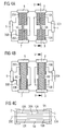
- FIGS. 1A to 1F show various views in plan view Layers of a device according to the invention, in which interconnection structures or internal electrodes are arranged. These figures each show the interconnection structure or internal electrodes disposed in the respective layer are and additionally for the sake of clarity and around the relative arrangement of the various electrical Clarify structures in the component, including the internal electrodes, each arranged in underlying layers are. Between layers in which internal electrodes or interconnection structures are arranged, respectively Any number of ceramic layers may be arranged, in which No internal electrodes or interconnection structures available are.
- FIGS. 1A to 1F show a sequence of FIGS Layers from top to bottom in the main body of the device, beginning with FIG. 1A and ending with FIG. 1F. this It can be seen from FIGS.
- an inner electrode 30, the electrically conductive with two outer contact layers. 5 and 4 is connected, overlapped with four electrode stacks, namely the electrode stack 10, consisting of the internal electrodes 10A and 10B connected to the outer contact layer 2, the electrode stack 15, consisting of the internal electrodes 15A and 15B in contact with the outer contact layer 3, the Electrode stack 20 of the inner electrodes 20A and 20B with the outer contact surface 7 and the electrode stack 25, the from the electrode layers 25A, 25B and the contact layer 6 consists.
- the electrode stacks 10 and 15 are electrically conductive via two meander-shaped interconnection structures 5A and 5B connected.
- the other two electrode stacks 25 and 20 are also over two meandering interconnection structures 5C and 5D interconnected.
- the meandering Interconnection structures have a particularly high inductance on. But are also possible differently shaped Interconnection structures, e.g. in the form of stripes.
- This Component according to the invention has two planes of symmetry on, a plane of symmetry 300 perpendicular to the ceramic Layers, which are drawn in all supervisory figures 1A to 1 F. is and one parallel to a ceramic layer extending symmetry plane 200, which is shown in Figure 1G is. These two planes of symmetry each form the interconnection structures and the internal electrodes from each other.
- FIG. 1G shows a cross section through which A in FIG. 1A designated section. It can be seen that the electrode stack 10 and 15 between the two the electrode stacks connecting meander-shaped interconnection structures 5A and 5B are arranged and the plane of symmetry 200 z. B. the interconnect structure 5A to the interconnection structure 5B and the inner electrode 15A images on the inner electrode 15B.
- FIG. 2 shows another embodiment in plan view a device according to the invention, in which, in contrast to in FIG. 1A to 1G, the electrode 30 in FIG two electrodes 30A and 30B is divided, each only overlap with two electrode stacks so that another internal Interconnection results. Only the two are top interconnect structures 5A and 5C, but not the respectively analogous interconnection structures in the lower area of the device.
- FIG. 3 shows an equivalent circuit diagram of the electrical component shown in FIG. 2 in plan view.
- the ⁇ filters shown in FIG. 3 can be realized. This results in each case a parallel connection of a capacitor effect 35 and a varistor effect 40, wherein additionally due to the two interconnection structures 5A, 5B and 5C, 5D, the parallel circuit of the capacitor and varistor effect is interconnected, wherein additionally a parallel connection of the resistors 5C and 5D or 5A and 5B result.
- the resistors are realized particularly advantageously by the meander-shaped interconnection structures shown, for example, in FIGS. 1A and 1F. It is also possible, however, to provide other forms for the interconnection structures, for example strips, and to form these from a material which has a high electrical resistance, for example RuO 2 .
- FIGS. 4A and 4B show plan views of further variants a component according to the invention, in which the Electrode stacks 10 and 15 of two differently shaped Wiring structures 5A and 5B electrically conductive get connected.
- the Interconnection structures as strips with straight course formed, wherein the interconnection structure 5A a has smaller width than the interconnect structure 5B.
- Figure 4C shows a cross-section through that with V in the figure 4A designated section. It can be seen that the strip-shaped interconnection structures 5 A and 5 B and z. B. the internal electrodes 15A, 15B by means of a plane of symmetry 200 can be imaged on each other.
- FIG. 5 shows another embodiment of a device according to the invention electrical component in cross section, the two Interconnection structures 5A and 5B as layer areas formed opposite surfaces of the body are.
- FIG. 6 shows another advantageous variant of a device according to the invention Component in the supervision of the interconnection structures 5A and 5C. It can be seen that this Interconnection structures 5A and 5C each that area cover in which the electrode 30A with the electrodes 15A and 10A and the electrode 30B with the electrodes 25A and 20A, respectively overlaps. If at least one or better still two Interconnection structures in this form two Connect electrode stacks together, these can be Electrode stack particularly advantageous over a Shield the board on which the component is mounted can. This has the consequence that the influence of the component position strong on the electrical properties of the device is reduced.
- Figure 7 shows an advantageous arrangement of a variant an electrical component according to the invention on a Substrate 100. It can be seen that the interconnection structure 5B between the substrate, the circuit board 100 and the Internal electrode stacks 10 and 15 is arranged. Through this special arrangement comes a particularly good shielding Internal electrode stacks 10 and 15 with respect to the substrate 100 conditions.
- the device 1 according to the invention can order 180 ° are rotated about the plane of symmetry 200, in which case the Interconnection structure 5A between the board 100 and the internal electrode stacks 10 and 15 would be arranged. Also at one Such rotated by 180 ° positioning can at similar to an electrical component according to the invention electrical properties are expected as in the in FIG 7 arrangement shown.
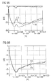
- Figure 8A shows the influence of the position of a conventional component with only one interconnect structure and no symmetry levels in the main body relative to a circuit board on the Damping behavior of the component.
- the component is as ⁇ filter executed.
- the two labeled 110 and 120 respectively Lines show the different damping behavior of the component when it is rotated 180 ° about its longitudinal axis and mounted on a circuit board. It can be seen that the different by 180 ° orientations of the component a great influence on the damping behavior of the conventional Have ⁇ filters.
- FIG. 8B shows the damping behavior of a device according to the invention ⁇ filters, in which two interconnection structures two electrode stacks Interconnect internally and in addition the two planes of symmetry are present, e.g. in Fig. 1A to 1G.
- the lines labeled 110 and 120, respectively respectively In doing so, the damping behavior is reversed by 180 ° for two the longitudinal axis rotated positions of the component on the board at. It can be clearly seen that the two different Positions in components according to the invention only show a small influence on the damping behavior.
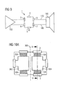
- Figure 9 shows a circuit in which an inventive electrical component 1 between an amplifier 150 and a noise sensitive device 160, such as a Speaker is switched.
- the amplifier 150 and the interference-sensitive Device 160 are via leads 170, 180th connected, wherein between the leads, the inventive Component 1 is connected.
- the outer contact layers 2, 3, 4, 5, 6 and 7 of the electrical component according to the invention refer to those in Figures 2 and 3 shown outer contact layers.
- the outer contact layer 5 is connected to the earth.
- Both high-frequency interference as for example in mobile devices over the Carrier frequency of some 100 to 10,000 MHz occur as also electrostatic discharges, which short-term pulses can generate high voltages through the device 1 safely before the device 160 are discharged to earth, wherein the useful signals, in the example of Figure 9 speech signals with a few kHz unhindered from the amplifier 150 to the device 160 can go through.
- the invention is possible with respect to the number of interconnection structures with each other connected electrode stack possible.
- Such a device has due to the shield of the Internal electrodes of the first and second electrode stack by two internal electrodes of the third electrode stack also a reduced influence of the positioning of the Component on the electrical properties in an outer Circuit environment (see, e.g., Figures 10A to 10C).
- the device is symmetrical with respect to the at least one interconnection structure and internal electrodes formed to a first level and a second level, the first plane being parallel and the second plane being vertical extends to a ceramic layer.
- the at least one interconnection structure is formed as a structured layer on the ceramic layers.
- Such an embodiment has the advantage that the interconnection structures can be produced particularly easily on the ceramic layers, for example by means of screen printing.
- the interconnection structures can be generated from conductive pastes.
- the interconnection structures can contain silver, palladium, platinum, copper, nickel or an alloy of silver and palladium or of silver and platinum, similar to the internal electrodes. Interconnection structures produced from such metals or metal alloys enable low-resistance interconnections.
- the interconnection structures to contain RuO 2 , Bi 2 Ru 2 O 7 , C, Ti 2 N or LaB 6 .
- At least two interconnection structures be present, the two electrode stacks with each other connect, so that an internal interconnection results.
- a first and second interconnect structure be present, which are formed so that they from above or At the bottom, at least the area in which the two electrode stacks overlap with the third electrode stack, covering.
- a result is particularly advantageous double shielding of the inner electrodes of the first and second Electrode stack through the inner electrodes of the third Electrode stack and wiring structures.
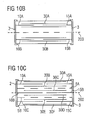
- 10A to 10C show a device according to the invention in Cross section and in the supervision.
- Fig. 10A shows in plan view two internal electrodes 30A, 30C of two third electrode stacks, each with the internal electrodes 10A, 15A and 20A, 25A of first and second, respectively Overlap electrode stacks.
- Figs. 10B and 10C respectively show Cross sections through two different variants of the Component through the designated V in Fig. 10A section. Both variants have the plan view shown in FIG. 10A and differ in the number of interconnection structures 5A, 5B, and the number of internal electrodes each Electrode stack can be seen as in the cross sections. It It can be seen that in Fig. 10B, two internal electrodes 30A, 30B a third electrode stack are arranged so that the Internal electrodes 15A, 15B and 10A, 10B disposed between them are.
- Fig. 10C shows a larger number of Inner selector electrodes per electrode stack, where additionally two Interconnection structures 5A, 5B are present and the interconnection structures and the internal electrodes of the electrode stack 10, 10A, 10B, 10C and the internal electrodes of the Electrode stack 15, 15A, 15B, 15C between the two outermost Internal electrodes 30A, 30F of the third electrode stack are arranged.
- both variants have the planes of symmetry 200 and 300 on.
Abstract
Description
Die Erfindung betrifft ein elektrisches Bauelement mit einem Grundkörper, der eine Abfolge von übereinandergestapelten keramischen Schichten umfaßt und mehrere zwischen den keramischen Schichten angeordnete Innenelektroden enthält.The invention relates to an electrical component with a Basic body, which is a succession of stacked ceramic Includes layers and several between the ceramic Layers arranged inner electrodes contains.
Aus der Druckschrift JP 10097954 A ist ein elektrisches Bauelement der eingangs genannten Art bekannt, bei dem zusätzlich zu den Innenelektroden auch Widerstandsstrukturen vorhanden sind, die eine interne Verschaltung bewirken können.From the document JP 10097954 A is an electrical component of the type mentioned above, in addition to to the internal electrodes also resistor structures available are that can cause an internal interconnection.
Die Erfinder haben überraschenderweise gefunden, daß diese Bauelemente in Abhängigkeit von ihrer Lageposition auf einer Leiterplatte unterschiedliche elektrische Eigenschaften, z.B. unterschiedliche Filtercharakteristiken aufweisen können.The inventors have surprisingly found that these Components depending on their position on a PCB different electrical properties, e.g. may have different filter characteristics.
Ziel der vorliegenden Erfindung ist es daher, ein elektrisches Bauelement anzugeben, das gegenüber des oben genannten Nachteils verbessert ist.The aim of the present invention is therefore an electric Specify component, which compared to the above Disadvantage is improved.
Dieses Ziel wird erfindungsgemäß durch ein elektrisches Bauelement nach Anspruch 1 oder alternativ nach Anspruch 13 erreicht. Vorteilhafte Ausgestaltungen des Bauelements sowie eine Schaltungsanordnung mit dem Bauelement sind Gegenstand weiterer Ansprüche. Im folgenden wird zuerst das erfindungsgemäße Bauelement nach Anspruch 1, sowie dessen vorteilhafte Ausgestaltungen dargestellt.This object is achieved by an electrical component according to claim 1 or alternatively achieved according to claim 13. Advantageous embodiments of the device as well a circuit arrangement with the component are the subject further claims. The following is the first invention Component according to claim 1, as well as its advantageous Embodiments shown.
Ein erfindungsgemäßes elektrisches Bauelement nach Anspruch 1 hat folgende Merkmale:
- ein Grundkörper, der eine Abfolge von übereinandergestapelten keramischen Schichten umfaßt, ist vorhanden,
- mehrere jeweils zwischen zwei keramischen Schichten angeordnete Innenelektroden sind vorhanden,
- auf der Oberfläche des Grundkörpers angeordnete Kontaktflächen, die elektrisch leitend mit den Innenelektroden verbunden sind, sind vorhanden, wobei Innenelektroden, die mit derselben Kontaktfläche verbunden sind, einen Elektrodenstapel bilden,
- wenigstens eine Verschaltungsstruktur, die zwei Elektrodenstapel miteinander verbindet ist vorhanden,
- das Bauelement ist symmetrisch bezüglich der wenigstens einen Verschaltungsstruktur und der Innenelektroden zu einer ersten Ebene und einer zweiten Ebene gebildet, wobei die erste Ebene parallel und die zweite Ebene senkrecht zu einer keramischen Schicht verläuft.
- a base body comprising a sequence of stacked ceramic layers is present,
- several internal electrodes each arranged between two ceramic layers are present,
- Contact surfaces arranged on the surface of the main body, which are electrically conductively connected to the internal electrodes, are present, internal electrodes, which are connected to the same contact area, forming an electrode stack.
- at least one interconnection structure that connects two electrode stacks with one another is present,
- the component is formed symmetrically with respect to the at least one interconnection structure and the inner electrodes to a first plane and a second plane, wherein the first plane is parallel and the second plane is perpendicular to a ceramic layer.
Bei einem derartigen erfindungsgemäßen Bauelement ist aufgrund der besonders hohen Symmetrie der Einfluß der Positionierung des Bauteils auf die elektrischen Eigenschaften in einer äußeren Schaltungsumgebung, z.B. auf einer Platine, gegenüber herkömmlichen Bauelementen verringert.In such a device according to the invention is due to particularly high symmetry the influence of positioning of the component on the electrical properties in an external circuit environment, e.g. on a circuit board, opposite reduced conventional components.
In einer vorteilhaften Ausführungsform überlappt bei einem erfindungsgemäßen elektrischen Bauelement zumindest eine Innenelektrode mit den Innenelektroden von wenigstens zwei weiteren Elektrodenstapeln. Eine derartige Ausführungsform hat den Vorteil, daß auf sehr kleinem Volumen viele miteinander überlappende Elektrodenstapel gebildet werden können, so daß eine hohe Integrationsdichte von elektrischen Strukturen im Bauelement resultiert. Die wenigstens eine Innenelektrode, die mit wenigstens zwei weiteren Elektrodenstapeln überlappt, kann beispielsweise über eine auf der Oberfläche des Grundkörpers angeordnete Kontaktfläche kontaktiert werden und als Masseanschluß für zwei Elektrodenstapel dienen, so daß zwei Vielschichtkondensatoren mit einem gemeinsamen Masseanschluß resultieren (siehe beispielsweise Figur 1G). Die zumindest eine Innenelektrode kann aber auch mit mehr als zwei Elektrodenstapeln überlappen. Die zumindest eine Innenelektrode kann aber auch Teil eines Elektrodenstapels sein, mit der Folge, daß dann ein Elektrodenstapel mit zumindest zwei anderen Elektrodenstapeln überlappt.In an advantageous embodiment overlaps in a inventive electrical component at least one inner electrode with the internal electrodes of at least two others Electrode stacks. Such an embodiment has the advantage that on very small volume many together overlapping electrode stacks can be formed so that a high integration density of electrical structures in the Component results. The at least one inner electrode, which overlaps with at least two further electrode stacks, For example, you can have one on the surface of the body arranged contact surface are contacted and as Ground connection serve for two electrode stacks, so that two Multilayer capacitors with a common ground connection result (see for example Figure 1G). The least an internal electrode can also be used with more than two electrode stacks overlap. The at least one inner electrode can but also part of an electrode stack, with the result that then an electrode stack with at least two others Electrode stacks overlap.
Weiterhin ist es möglich, daß die wenigstens eine Verschaltungsstruktur als strukturierte Schicht auf den keramischen Schichten ausgebildet ist. Eine derartige Ausführungsform hat den Vorteil, daß die Verschaltungsstrukturen z.B. mittels Siebdruck besonders einfach auf den keramischen Schichten erzeugt werden können. Die Verschaltungsstrukturen können dabei aus leitfähigen Pasten erzeugt werden. Die Verschaltungsstrukturen können dabei ähnlich wie die Innenelektroden Silber, Palladium, Platin, Kupfer, Nickel oder eine Legierung aus Silber und Palladium oder aus Silber und Platin enthalten. Aus derartigen Metallen bzw. Metallegierungen hergestellte Verschaltungsstrukturen ermöglichen niederohmige Verschaltungen. Zur Generierung von hochohmigen Verschaltungsstrukturen ist es beispielsweise auch möglich, daß die Verschaltungsstrukturen RuO2, Bi2Ru2O7, C, Ti2N oder LaB6 enthalten.Furthermore, it is possible that the at least one interconnection structure is formed as a structured layer on the ceramic layers. Such an embodiment has the advantage that the interconnection structures can be produced particularly easily on the ceramic layers, for example by means of screen printing. The interconnection structures can be generated from conductive pastes. The interconnection structures can contain silver, palladium, platinum, copper, nickel or an alloy of silver and palladium or of silver and platinum, similar to the internal electrodes. Interconnection structures produced from such metals or metal alloys enable low-resistance interconnections. For example, to generate high-resistance interconnection structures, it is also possible for the interconnection structures to contain RuO 2 , Bi 2 Ru 2 O 7 , C, Ti 2 N or LaB 6 .
Vorteilhafterweise kann dabei die zumindest eine Verschaltungsstruktur im Inneren des Grundkörpers zwischen unterschiedlichen Paaren von keramischen Schichten angeordnet sein. Eine derartige Ausführungsform ist z.B. in Figur 1G gezeigt. Möglich ist es aber auch, daß im Falle von zwei Verschaltungsstrukturen diese auf sich gegenüberliegenden Oberflächen des Grundkörpers angeordnet sind, wie z.B. in Figur 5 gezeigt.Advantageously, the at least one interconnection structure can be used inside the body between different Pairs of ceramic layers arranged be. Such an embodiment is e.g. shown in Figure 1G. But it is also possible that in the case of two interconnection structures these on opposite surfaces of the main body are arranged, e.g. in FIG. 5 shown.
Günstigerweise sind im Fall von wenigstens zwei Verschaltungsstrukturen diese so im oder auf dem Grundkörper angeordnet, daß die Innenelektroden derjenigen Elektrodenstapel, die durch die Verschaltungsstrukturen verbunden sind, zwischen den beiden Verschaltungsstrukturen im Grundkörper angeordnet sind. Eine derartige Anordnung von Verschaltungsstrukturen und Innenelektroden ist beispielsweise in den Figuren 1G und 5 gezeigt. In diesem Fall schirmen die vorteilhafterweise oberhalb bzw. unterhalb der Innenelektroden angeordneten Verschaltungsstrukturen die Innenelektroden gegenüber einer Platine, auf die das Bauelement montiert wird, besonders gut ab, so daß erneut eine Reduzierung des Einflusses der Positionierung des Bauelements auf die elektrischen Eigenschaften resultiert.Conveniently, in the case of at least two interconnection structures these are arranged in or on the base body, in that the internal electrodes of those electrode stacks which are interconnected by the interconnection structures arranged the two interconnection structures in the main body are. Such an arrangement of interconnection structures and internal electrodes, for example, in Figures 1G and 5 shown. In this case, they are advantageously shielded above or below the internal electrodes arranged interconnection structures the internal electrodes opposite a circuit board, on which the component is mounted, particularly good, so again reducing the influence of positioning of the device results in the electrical properties.
In einer weiteren Variante des erfindungsgemäßen Bauelements ist eine erste Verschaltungsstruktur zwischen zwei im oberen Bereich des Grundkörpers und eine zweite Verschaltungsstruktur zwischen zwei im unteren Bereich des Grundkörpers befindlichen keramischen Schichten angeordnet, wobei diese erste und zweite Verschaltungsstruktur zwei im Grundkörper gegenüberliegende Elektrodenstapel miteinander verbinden. Die zwei Elektrodenstapel überlappen dabei mit einem dritten Elektrodenstapel, wobei die Innenelektroden der zwei Elektrodenstapel, die durch die Verschaltungsstrukturen verbunden sind, zwischen der ersten und zweiten Verschaltungsstruktur im Grundkörper angeordnet sind. Eine derartige relative Anordnung der Verschaltungsstrukturen und Innenelektroden erlaubt eine besonders hohe Integrationsdichte von elektrischen Strukturen im erfindungsgemäßen elektrischen Bauelement, wobei gleichzeitig eine besonders geringe Abhängigkeit der elektrischen Eigenschaften des Bauelements von seiner Lage auf der Platine erreicht werden kann.In a further variant of the component according to the invention is a first interconnection structure between two in the upper Area of the body and a second interconnection structure between two located in the lower part of the body arranged ceramic layers, said first and second interconnection structure two in the main body opposite Connect electrode stack together. The two Electrode stacks overlap with a third electrode stack, wherein the internal electrodes of the two electrode stacks, which are connected by the interconnection structures, between the first and second interconnection structure in Basic body are arranged. Such a relative arrangement the interconnection structures and internal electrodes allowed a particularly high integration density of electrical Structures in the electrical component according to the invention, wherein at the same time a particularly low dependence of electrical properties of the device of its location can be achieved on the board.
Vorteilhafterweise sind die Verschaltungsstrukturen so ausgeformt, daß sie von oben oder von unten auf den Grundkörper aus übereinandergestapelten Schichten betrachtet zumindest den Bereich abdecken, in dem die zwei Elektrodenstapel mit dem dritten Elektrodenstapel überlappen. Eine Aufsicht auf eine derart ausgestaltete Verschaltungsstruktur ist beispielsweise in der Figur 6 gezeigt. In dem Fall, daß in der Aufsicht auf die Verschaltungsstrukturen der Überlappungsbereich zwischen den Elektrodenstapeln abgedeckt ist, resultiert eine besonders gute Abschirmung der Innenelektroden gegenüber der Platine, auf der das Bauelement montiert werden kann. Derartige Bauelemente weisen daher einen besonders geringen Einfluß ihrer Lageposition auf der Platine auf die elektrischen Eigenschaften auf.Advantageously, the interconnection structures are like this formed that they from above or from below on the Basic body viewed from stacked layers at least cover the area where the two electrode stacks overlap with the third electrode stack. A view of such a configured interconnection structure is shown for example in FIG. By doing Case that, in supervision, the interconnection structures of the Overlapping area covered between the electrode stacks is, results in a particularly good shielding of the internal electrodes opposite the board on which the component is mounted can be. Such components therefore have a particularly low influence of their position on the board on the electrical properties.
In einer weiteren Variante eines erfindungsgemäßen Bauelements überlappen ein erster und ein zweiter Elektrodenstapel mit einem dritten Elektrodenstapel, wobei die Innenelektroden des ersten und zweiten Elektrodenstapels zwischen zwei Innenelektroden des dritten Elektrodenstapels im Grundkörper angeordnet sind. Bei einem derartigen Bauelement ergibt sich ein zusätzlicher Abschirmeffekt für die Innenelektroden des ersten und zweiten Elektrodenstapels dadurch, daß sie zwischen zwei Innenelektroden des dritten Elektrodenstapels angeordnet sind.In a further variant of a component according to the invention overlap a first and a second electrode stack with a third electrode stack, wherein the internal electrodes of the first and second electrode stacks between two internal electrodes of the third electrode stack in the main body are arranged. In such a device results an additional shielding effect for the internal electrodes of the first and second electrode stack in that they are between two internal electrodes of the third electrode stack are arranged are.
Der Grundkörper eines erfindungsgemäßen elektrischen Bauelements kann entlang einer Längsrichtung verlaufende Seitenflächen und mindestens eine Stirnfläche aufweisen, wobei dann durch zwei überlappende Elektrodenstapel ein Vielschichtkondensator gebildet ist und die Kontaktfläche eines überlappenden Elektrodenstapels des Vielschichtkondensators auf einer Seitenfläche und die Kontaktfläche des anderen überlappenden Elektrodenstapels des Vielschichtkondensators auf der Stirnfläche des Grundkörpers angeordnet ist. Eine derartige Anordnung von Kontaktflächen für die Elektrodenstapel auf der Oberfläche des Grundkörpers ist besonders vorteilhaft und ermöglicht eine besonders hohe Dichte von Kontaktflächen auf dem Grundkörper, wobei dann auch besonders einfach eine hohe Integrationsdichte von Elektrodenstapeln im Grundkörper von erfindungsgemäßen Bauelementen verwirklicht werden kann.The main body of an electrical component according to the invention can be along a longitudinal direction extending side surfaces and at least one end face, in which case through two overlapping electrode stacks a multilayer capacitor is formed and the contact surface of a overlapping electrode stack of the multilayer capacitor on one side surface and the contact surface of the other overlapping electrode stack of the multilayer capacitor is arranged on the end face of the base body. A Such arrangement of contact surfaces for the Electrode stack on the surface of the body is particularly advantageous and allows a particularly high Density of contact surfaces on the body, in which case also particularly easy a high integration density of electrode stacks in the main body of components according to the invention can be realized.
Zur Erzielung einer besonders hohen Integrationsdichte von Elektrodenstapeln im erfindungsgemäßen Bauelement ist es vorteilhaft, wenn die zumindest zwei Verschaltungsstrukturen zwei Elektrodenstapel miteinander verbinden, deren Kontaktflächen auf gegenüberliegenden Seitenflächen angeordnet sind und zumindest ein weiterer Elektrodenstapel mit den zwei Elektrodenstapeln überlappt, wobei dessen Kontaktfläche auf einer Stirnfläche des Grundkörpers angeordnet ist. Bei einer derartigen Anordnung von Elektrodenstapeln zueinander, wie sie beispielsweise in der Figur 2 in der Aufsicht gezeigt ist, ist es besonders leicht möglich, auf geringstem Raum zwei Vielschichtkondensatoren unterzubringen, die eine gemeinsame Kontaktfläche aufweisen.To achieve a particularly high integration density of Electrode stacks in the device according to the invention, it is advantageous if the at least two interconnection structures connect two electrode stacks with each other, their contact surfaces are arranged on opposite side surfaces and at least one more electrode stack with the two Electrode stacks overlap, with its contact surface on an end face of the base body is arranged. At a such arrangement of electrode stacks to each other, as they are shown for example in the figure 2 in the plan is, it is particularly easy, in the smallest space accommodate two multilayer capacitors, the one have common contact surface.
Um ein erfindungsgemäßes elektrisches Bauteil mit breitbandiger Filterfunktion zur Unterdrückung von Rauschsignalen zu erhalten, bilden zwei überlappende Elektrodenstapel jeweils einen Vielschichtkondensator, wobei zwei Paare von jeweils einander gegenüberliegenden Vielschichtkondensatoren mit jeweils zwei Verschaltungsstrukturen zwei Π-Filter bilden. Eine besondere Ausführungsform eines derartigen Π-Filters ist beispielsweise in Figur 3 gezeigt, wobei dort die zwischen den Innenelektroden angeordneten keramischen Schichten eine Varistorkeramik, z.B. auf der Basis von ZnO-Bi und/oder ZnO-Pr enthalten. Möglich wäre aber auch, daß die keramischen Schichten nur eine Kondensatorkeramik enthalten, so daß eine Schaltungsanordnung ähnlich zu Figur 3 resultieren würde, bei der allerdings kein Varistoreffekt vorhanden wäre.To an inventive electrical component with broadband Filter function for suppressing noise signals too obtained, form two overlapping electrode stacks respectively a multilayer capacitor, with two pairs of each each opposed multilayer capacitors two interconnection structures form two Π-filters. A particular embodiment of such a Π-filter For example, shown in Figure 3, where between the the inner electrodes arranged ceramic layers a Varistor ceramic, e.g. based on ZnO-Bi and / or ZnO-Pr contain. But it would also be possible that the ceramic Layers only contain a capacitor ceramic, so that a Circuit arrangement would result similar to Figure 3, at however, no varistor effect would be present.
Im Falle von wenigstens zwei Verschaltungsstrukturen im oder auf dem Grundkörper wird ein erfindungsgemäßes Bauelement vorteilhafterweise so auf einem Substrat orientiert, daß wenigstens eine Verschaltungsstruktur zwischen dem Substrat und den Innenelektroden der Elektrodenstapel angeordnet ist, die von den Verschaltungsstrukturen verbunden sind. Eine derartige Anordnung aus einem erfindungsgemäßen elektrischen Bauelement und einem Substrat ist beispielsweise in Figur 7 gezeigt.In the case of at least two interconnection structures in or on the body is a device according to the invention advantageously so oriented on a substrate that at least a wiring structure between the substrate and the inner electrodes of the electrode stack is arranged, the connected by the interconnection structures. Such Arrangement of an electrical component according to the invention and a substrate is shown in FIG. 7, for example.
Im folgenden soll das erfindungsgemäße elektrische Bauelement anhand von Ausführungsbeispielen und Figuren noch näher erläutert werden. Bei den Figuren handelt es sich dabei um vereinfachte schematische Zeichnungen.
- Die Figuren 1A bis 1G
- zeigen Aufsichten und einen Querschnitt eines erfindungsgemäßen elektrischen Bauelements.
- Die
Figur 2 - zeigt eine Aufsicht auf eine weitere Variante eines erfindungsgemäßen elektrischen Bauelements.
- Die
Figur 3 - zeigt ein Schaltbild eines erfindungsgemäßen elektrischen Bauelements.
- Die Figuren 4A bis 4C
- zeigen verschiedene Ausführungsformen der Verschaltungsstrukturen in der Aufsicht und im Querschnitt.
Figur 5- zeigt eine weitere Ausführungsform eines erfindungsgemäßen Bauelements im Querschnitt.
Figur 6- zeigt eine andere Variante eines elektrischen Bauelements in der Aufsicht.
Figur 7- zeigt im Querschnitt eine Anordnung aus einem erfindungsgemäßen elektrischen Bauelement und einer Platine.
- Die Figuren 8A und 8B
- zeigen Meßdiagramme elektrischer Eigenschaften eines herkömmlichen und eines erfindungsgemäßen Bauelements.
- Figur 9
- zeigt eine Schaltungsanordnung, bei der ein erfindungsgemäßes Bauelement zwischen einem Verstärker und einem störungsempfindlichen Gerät geschaltet ist.
- Figures 1A to 1G
- show views and a cross section of an electrical component according to the invention.
- The figure 2
- shows a plan view of a further variant of an electrical component according to the invention.
- The figure 3
- shows a circuit diagram of an electrical component according to the invention.
- FIGS. 4A to 4C
- show various embodiments of the interconnection structures in the plan and in cross section.
- FIG. 5
- shows a further embodiment of a device according to the invention in cross section.
- FIG. 6
- shows another variant of an electrical component in the supervision.
- FIG. 7
- shows in cross section an arrangement of an electrical component according to the invention and a circuit board.
- Figures 8A and 8B
- show measuring diagrams of electrical properties of a conventional and a device according to the invention.
- FIG. 9
- shows a circuit arrangement in which a device according to the invention is connected between an amplifier and a noise-sensitive device.
Die Figuren 1A bis 1F zeigen in der Aufsicht verschiedene
Schichten eines erfindungsgemäßen Bauelements, in denen Verschaltungsstrukturen
bzw. Innenelektroden angeordnet sind.
Diese Figuren zeigen dabei jeweils die Verschaltungsstruktur
bzw. Innenelektroden, die in der jeweiligen Schicht angeordnet
sind und zusätzlich aus Gründen der Anschaulichkeit und
um die relative Anordnung der verschiedenen elektrischen
Strukturen im Bauelement zu verdeutlichen, auch die Innenelektroden,
die jeweils in darunterliegenden Schichten angeordnet
sind. Zwischen Schichten, in denen Innenelektroden
bzw. Verschaltungsstrukturen angeordnet sind, können jeweils
beliebig viele keramische Schichten angeordnet sein, in denen
keine Innenelektroden bzw. Verschaltungsstrukturen vorhanden
sind. Die Figuren 1A bis 1F stellen dabei eine Abfolge der
Schichten von oben nach unten im Grundkörper des Bauelements,
beginnend mit Figur 1A und endend mit der Figur 1F. Diesen
Figuren ist dabei zu entnehmen, daß eine Innenelektrode 30,
die elektrisch leitend mit zwei äußeren Kontaktschichten 5
und 4 verbunden ist, mit vier Elektrodenstapeln überlappt,
nämlich dem Elektrodenstapel 10, bestehend aus den Innenelektroden
10A und 10B, verbunden mit der äußeren Kontaktschicht
2, dem Elektrodenstapel 15, bestehend aus den Innenelektroden
15A und 15B in Kontakt mit der äußeren Kontaktschicht 3, dem
Elektrodenstapel 20 aus den Innenelektroden 20A und 20B mit
der äußeren Kontaktfläche 7 und dem Elektrodenstapel 25, der
aus den Elektrodenschichten 25A, 25B und der Kontaktschicht 6
besteht. Die Elektrodenstapel 10 und 15 sind elektrisch leitend
über zwei mäanderförmige Verschaltungsstrukturen 5A und
5B verbunden. Die anderen beiden Elektrodenstapel 25 und 20
sind ebenfalls über zwei mäanderförmige Verschaltungsstrukturen
5C und 5D miteinander verschaltet. Die mäanderförmigen
Verschaltungsstrukturen weisen dabei eine besonders hohe Induktivität
auf. Möglich sind aber auch anders ausgeformte
Verschaltungsstrukturen, z.B. in der Form von Streifen. Dieses
erfindungsgemäße Bauelement weist zwei Symmetrieebenen
auf, eine Symmetrieebene 300 senkrecht zu den keramischen
Schichten, die in allen Aufsichtsfiguren 1A bis 1 F eingezeichnet
ist und eine parallel zu einer keramischen Schicht
verlaufende Symmetrieebene 200, die in Figur 1G eingezeichnet
ist. Diese beiden Symmetrieebenen bilden jeweils die Verschaltungsstrukturen
und die Innenelektroden aufeinander ab.FIGS. 1A to 1F show various views in plan view
Layers of a device according to the invention, in which interconnection structures
or internal electrodes are arranged.
These figures each show the interconnection structure
or internal electrodes disposed in the respective layer
are and additionally for the sake of clarity and
around the relative arrangement of the various electrical
Clarify structures in the component, including the internal electrodes,
each arranged in underlying layers
are. Between layers in which internal electrodes
or interconnection structures are arranged, respectively
Any number of ceramic layers may be arranged, in which
No internal electrodes or interconnection structures available
are. FIGS. 1A to 1F show a sequence of FIGS
Layers from top to bottom in the main body of the device,
beginning with FIG. 1A and ending with FIG. 1F. this
It can be seen from FIGS. That an
Figur 1G zeigt einen Querschnitt, durch den in Figur 1A mit A
bezeichneten Schnitt. Dabei ist zu erkennen, daß die Elektrodenstapel
10 und 15 zwischen den beiden die Elektrodenstapel
verbindenden mäanderförmigen Verschaltungsstrukturen 5A und
5B angeordnet sind und die Symmetrieebene 200 z. B. die Verschaltungsstruktur
5A auf die Verschaltungsstruktur 5B und
die Innenelektrode 15A auf die Innenelektrode 15B abbildet.FIG. 1G shows a cross section through which A in FIG. 1A
designated section. It can be seen that the
Figur 2 zeigt in der Aufsicht eine weitere Ausführungsform
eines erfindungsgemäßen Bauelements, bei dem im Gegensatz zum
in Figur 1A bis 1G gezeigten Bauelement die Elektrode 30 in
zwei Elektroden 30A und 30B aufgeteilt ist, die jeweils nur
mit zwei Elektrodenstapeln überlappen, so daß eine andere interne
Verschaltung resultiert. Dabei sind nur die beiden
obersten Verschaltungsstrukturen 5A und 5C gezeigt, aber
nicht die jeweils dazu analogen Verschaltungsstrukturen im
unteren Bereich des Bauelements.FIG. 2 shows another embodiment in plan view
a device according to the invention, in which, in contrast to
in FIG. 1A to 1G, the
Figur 3 zeigt ein Ersatzschaltbild des in der Figur 2 in der
Aufsicht gezeigten elektrischen Bauelements. Unter Verwendung
einer Varistorkeramik für die keramischen Schichten zwischen
den Innenelektroden lassen sich die in Figur 3 gezeigten Π-Filter
realisieren. Dabei resultiert jeweils eine Parallelschaltung
eines Kondensatoreffekts 35 und eines Varistoreffekts
40, wobei zusätzlich aufgrund der zwei Verschaltungsstrukturen
5A, 5B bzw. 5C, 5D, die Parallelschaltung aus dem
Kondensator- und Varistoreffekt miteinander verschaltet ist,
wobei zusätzlich eine Parallelschaltung der Widerstände 5C
und 5D bzw. 5A und 5B resultiert. Die Widerstände werden besonders
vorteilhaft durch die z.B. in den Figuren 1A und 1F
gezeigten mäanderförmigen Verschaltungsstrukturen realisiert.
Möglich ist es aber auch, andere Formen für die Verschaltungsstrukturen,
z.B. Streifen vorzusehen und diese aus einen
Material auszubilden, daß einen hohen elektrischen Widerstand
aufweist, z.B. RuO2.FIG. 3 shows an equivalent circuit diagram of the electrical component shown in FIG. 2 in plan view. By using a varistor ceramic for the ceramic layers between the internal electrodes, the Π filters shown in FIG. 3 can be realized. This results in each case a parallel connection of a
Die Figuren 4A und 4B zeigen Aufsichten auf weitere Varianten
eines erfindungsgemäßen Bauelements, bei dem die
Elektrodenstapel 10 und 15 von zwei verschieden ausgeformten
Verschaltungsstrukturen 5A und 5B elektrisch leitend
verbunden werden. In diesem Fall sind die
Verschaltungsstrukturen als Streifen mit geradlinigem Verlauf
ausgebildet, wobei die Verschaltungsstruktur 5A eine
geringere Breite aufweist, als die Verschaltungsstruktur 5B.FIGS. 4A and 4B show plan views of further variants
a component according to the invention, in which the
Electrode stacks 10 and 15 of two differently shaped
Figur 4C zeigt einen Querschnitt durch den mit V in der Figur
4A bezeichneten Schnitt. Es ist zu erkennen, daß auch die
streifenförmigen Verschaltungsstrukturen 5 A und 5B und z. B.
die Innenelektroden 15A, 15B mittels einer Symmetrieebene 200
aufeinander abgebildet werden können.Figure 4C shows a cross-section through that with V in the figure
4A designated section. It can be seen that the
strip-shaped
Figur 5 zeigt eine andere Ausführungsform eines erfindungsgemäßen
elektrischen Bauelements im Querschnitt, wobei die beiden
Verschaltungsstrukturen 5A und 5B als Schichtbereiche auf
gegenüberliegenden Oberflächen des Grundkörpers ausgebildet
sind.FIG. 5 shows another embodiment of a device according to the invention
electrical component in cross section, the two
Figur 6 zeigt eine andere vorteilhafte Variante eines erfindungsgemäßen
Bauelements in der Aufsicht auf die Verschaltungsstrukturen
5A und 5C. Dabei ist zu erkennen, daß diese
Verschaltungsstrukturen 5A und 5C jeweils denjenigen Bereich
abdecken, in dem die Elektrode 30A mit den Elektroden 15A und
10A bzw. die Elektrode 30B mit dem Elektroden 25A und 20A
überlappt. Wenn wenigstens eine oder besser noch zwei
Verschaltungsstrukturen in dieser Ausformung zwei
Elektrodenstapel miteinander verbinden, lassen sich diese
Elektrodenstapel besonders vorteilhaft gegenüber einer
Platine abschirmen, auf die das Bauelement montiert werden
kann. Dies hat zur Folge, daß der Einfluß der Bauteil-Lage
auf die elektrischen Eigenschaften des Bauelements stark
verringert wird.FIG. 6 shows another advantageous variant of a device according to the invention
Component in the supervision of the
Figur 7 zeigt eine vorteilhafte Anordnung aus einer Variante
eines erfindungsgemäßen elektrischen Bauelements auf einem
Substrat 100. Dabei ist zu erkennen, daß die Verschaltungsstruktur
5B zwischen dem Substrat, der Platine 100 und den
Innenelektrodenstapeln 10 bzw. 15 angeordnet ist. Durch diese
besondere Anordnung kommt eine besonders gute Abschirmung der
Innenelektrodenstapel 10 und 15 gegenüber dem Substrat 100
zustande. Das erfindungsgemäße Bauelement 1 kann dabei um
180° um die Symmetrieebene 200 gedreht werden, wobei dann die
Verschaltungsstruktur 5A zwischen der Platine 100 und den Innenelektrodenstapeln
10 und 15 angeordnet wäre. Auch bei einer
derartigen um 180° rotierten Positionierung können bei
einem erfindungsgemäßen elektrischen Bauelement ähnliche
elektrische Eigenschaften erwartet werden wie bei der in Figur
7 gezeigten Anordnung.Figure 7 shows an advantageous arrangement of a variant
an electrical component according to the invention on a
Figur 8A zeigt den Einfluß der Lage eines herkömmlichen Bauteils mit nur einer Verschaltungsstruktur und keinen Symmetrieebenen im Grundkörper relativ zu einer Platine auf das Dämpfungsverhalten des Bauteils. Das Bauteil ist dabei als Π-Filter ausgeführt. Die beiden mit 110 bzw. 120 bezeichneten Linien zeigen dabei das unterschiedliche Dämpfungsverhalten des Bauteils, wenn es um 180° um seine Längsachse gedreht und auf einer Platine montiert wird. Dabei ist zu erkennen, daß die um 180° unterschiedlichen Orientierungen des Bauteils einen großen Einfluß auf das Dämpfungsverhalten des herkömmlichen Π-Filters aufweisen.Figure 8A shows the influence of the position of a conventional component with only one interconnect structure and no symmetry levels in the main body relative to a circuit board on the Damping behavior of the component. The component is as Π filter executed. The two labeled 110 and 120 respectively Lines show the different damping behavior of the component when it is rotated 180 ° about its longitudinal axis and mounted on a circuit board. It can be seen that the different by 180 ° orientations of the component a great influence on the damping behavior of the conventional Have Π filters.
Figur 8B zeigt das Dämpfungsverhalten eines erfindungsgemäßen Π-Filters, bei dem zwei Verschaltungsstrukturen zwei Elektrodenstapel intern miteinander verschalten und zusätzlich die beiden Symmetrieebenen vorhanden sind, wie z.B. in Fig. 1A bis 1G gezeigt. Die mit 110 bzw. 120 bezeichneten Linien geben dabei wieder das Dämpfungsverhalten bei zwei um 180° um die Längsachse rotierten Positionen des Bauteils auf der Platine an. Deutlich ist zu erkennen, daß die beiden unterschiedlichen Positionen bei erfindungsgemäßen Bauteilen nur einen geringen Einfluß auf das Dämpfungsverhalten zeigen.FIG. 8B shows the damping behavior of a device according to the invention Π filters, in which two interconnection structures two electrode stacks Interconnect internally and in addition the two planes of symmetry are present, e.g. in Fig. 1A to 1G. The lines labeled 110 and 120, respectively In doing so, the damping behavior is reversed by 180 ° for two the longitudinal axis rotated positions of the component on the board at. It can be clearly seen that the two different Positions in components according to the invention only show a small influence on the damping behavior.
Figur 9 zeigt eine Schaltung, bei der ein erfindungsgemäßes
elektrisches Bauelement 1 zwischen einen Verstärker 150 und
einen störungsempfindlichen Gerät 160, beispielsweise einem
Lautsprecher geschaltet ist. Der Verstärker 150 und das störungsempfindliche
Gerät 160 sind über Zuleitungen 170, 180
verbunden, wobei zwischen die Zuleitungen das erfindungsgemäße
Bauelement 1 geschaltet ist. Die äußeren Kontaktschichten
2, 3, 4, 5, 6 und 7 des erfindungsgemäßen elektrischen Bauelements
beziehen sich dabei auf die in den Figuren 2 und 3
gezeigten äußeren Kontaktschichten. Die äußere Kontaktschicht
5 ist dabei mit der Erde verbunden. Sowohl hochfrequente Störungen,
wie sie beispielsweise in Mobilfunkgeräten über die
Trägerfrequenz von einigen 100 bis 10.000 MHz auftreten, als
auch elektrostatische Entladungen, welche kurzzeitige Pulse
mit hohen Spannungen generieren, können durch das Bauelement
1 sicher vor dem Gerät 160 zur Erde abgeleitet werden, wobei
die Nutzsignale, im Beispiel aus Figur 9 Sprachsignale mit
einigen KHz ungehindert vom Verstärker 150 zum Gerät 160
durchlaufen können.Figure 9 shows a circuit in which an inventive
electrical component 1 between an
Durch Verwenden eines geeigneten Keramikmaterials für die keramischen Schichten wird aus dem Vielschichtkondensator ein Vielschichtvaristor. Ebenso können durch Auswahl geeigneter Keramikmaterialien für die keramischen Schichten noch weitere Vielschichtbauelemente realisiert werden. Weitere Ausführungsbeispiele der Erfindung sind beispielsweise möglich hinsichtlich der Anzahl der durch Verschaltungsstrukturen miteinander verbundenen Elektrodenstapel möglich.By using a suitable ceramic material for the ceramic Layers are made of the multilayer capacitor Multilayer varistor. Likewise, by selecting appropriate Ceramic materials for the ceramic layers even more Multi-layer devices can be realized. Further embodiments For example, the invention is possible with respect to the number of interconnection structures with each other connected electrode stack possible.
Im folgenden wird das alternative Bauelement nach Anspruch 13 beschrieben, das ebenfalls einen verringerten Einfluß der Positionierung des Bauteils auf die elektrischen Eigenschaften in einer äußeren Schaltungsumgebung, z.B. auf einer Platine zeigt. Ein erfindungsgemäßes Bauelement nach Anspruch 13 weist folgende Merkmale auf:
- ein Grundkörper der eine Abfolge von übereinandergestapelten keramischen Schichten umfaßt ist vorhanden,
- mehrere jeweils zwischen zwei keramischen Schichten angeordnete Innenelektroden sind vorhanden,
- auf der Oberfläche des Grundkörpers sind Kontaktflächen angeordnet, die elektrisch leitend mit den Innenelektroden verbunden sind, wobei Innenelektroden die mit der derselben Kontaktfläche verbunden sind einen Elektrodenstapel bilden,
- wenigstens eine Verschaltungsstruktur, die zwei Elektrodenstapel miteinander verbindet ist vorhanden,
- ein erster und ein zweiter Elektrodenstapel überlappen mit einem dritten Elektrodenstapel, wobei die Innenelektroden des ersten und zweiten Elektrodenstapels zwischen zwei Innenelektroden des dritten Elektrodenstapels angeordnet sind.
- a base body comprising a sequence of stacked ceramic layers is present,
- several internal electrodes each arranged between two ceramic layers are present,
- contact surfaces are arranged on the surface of the main body and are electrically conductively connected to the internal electrodes, internal electrodes which are connected to the same contact area forming an electrode stack,
- at least one interconnection structure that connects two electrode stacks with one another is present,
- a first and a second electrode stack overlap with a third electrode stack, wherein the inner electrodes of the first and second electrode stack are arranged between two inner electrodes of the third electrode stack.
Ein derartiges Bauelement weist aufgrund der Abschirmung der Innenelektroden des ersten und zweiten Elektrodenstapels durch zwei Innenelektroden des dritten Elektrodenstapels ebenfalls einen verringerten Einfluß der Positionierung des Bauteils auf die elektrischen Eigenschaften in einer äußeren Schaltungsumgebung auf (siehe z.B. Fig. 10A bis 10C).Such a device has due to the shield of the Internal electrodes of the first and second electrode stack by two internal electrodes of the third electrode stack also a reduced influence of the positioning of the Component on the electrical properties in an outer Circuit environment (see, e.g., Figures 10A to 10C).
Vorteilhafterweise ist das Bauelement symmetrisch bezüglich der wenigstens einen Verschaltungsstruktur und Innenelektroden zu einer ersten Ebene und einer zweiten Ebene gebildet, wobei die erste Ebene parallel und die zweite Ebene senkrecht zu einer keramischen Schicht verläuft. Ein derartiges Bauelement weist zum einen aufgrund der Abschrirmung durch die Innenelektroden des dritten Elektrodenstapels und zum anderen aufgrund seiner hohen Symmetrie einen verringerten Einfluß der Positionierung des Bauteils auf die elektrischen Eigenschaften in einer äußeren Schaltungsumgebung auf.Advantageously, the device is symmetrical with respect to the at least one interconnection structure and internal electrodes formed to a first level and a second level, the first plane being parallel and the second plane being vertical extends to a ceramic layer. Such a device on the one hand due to the Abschrirmung by the internal electrodes the third electrode stack and the other due to its high symmetry a reduced influence the positioning of the component on the electrical properties in an external circuit environment.
Weiterhin ist es möglich, daß die wenigstens eine Verschaltungsstruktur als strukturierte Schicht auf den keramischen Schichten ausgebildet ist. Eine derartige Ausführungsform hat den Vorteil, daß die Verschaltungsstrukturen z.B. mittels Siebdruck besonders einfach auf den keramischen Schichten erzeugt werden können. Die Verschaltungsstrukturen können dabei aus leitfähigen Pasten erzeugt werden. Die Verschaltungsstrukturen können dabei ähnlich wie die Innenelektroden Silber, Palladium, Platin, Kupfer, Nickel oder eine Legierung aus Silber und Palladium oder aus Silber und Platin enthalten. Aus derartigen Metallen bzw. Metallegierungen hergestellte Verschaltungsstrukturen ermöglichen niederohmige Verschaltungen. Zur Generierung von hochohmigen Verschaltungsstrukturen ist es beispielsweise auch möglich, daß die Verschaltungsstrukturen RuO2, Bi2Ru2O7, C, Ti2N oder LaB6 enthalten.Furthermore, it is possible that the at least one interconnection structure is formed as a structured layer on the ceramic layers. Such an embodiment has the advantage that the interconnection structures can be produced particularly easily on the ceramic layers, for example by means of screen printing. The interconnection structures can be generated from conductive pastes. The interconnection structures can contain silver, palladium, platinum, copper, nickel or an alloy of silver and palladium or of silver and platinum, similar to the internal electrodes. Interconnection structures produced from such metals or metal alloys enable low-resistance interconnections. For example, to generate high-resistance interconnection structures, it is also possible for the interconnection structures to contain RuO 2 , Bi 2 Ru 2 O 7 , C, Ti 2 N or LaB 6 .
Vorteilhafterweise können wenigstens zwei Verschaltungsstrukturen vorhanden sein, die zwei Elektrodenstapel miteinander verbinden, so daß eine interne Verschaltung resultiert.Advantageously, at least two interconnection structures be present, the two electrode stacks with each other connect, so that an internal interconnection results.
Weiterhin können eine erste und zweite Verschaltungsstruktur vorhanden sein, die so ausgeformt sind, daß sie von oben oder unten betrachtet zumindest den Bereich in dem die zwei Elektrodenstapel mit dem dritten Elektrodenstapel überlappen, abdeckt. In diesem Fall resultiert besonders vorteilhaft eine doppelte Abschirmung der Innenelektroden des ersten und zweiten Elektrodenstapels durch die Innenelektroden des dritten Elektrodenstapels und der Verschaltungsstrukturen.Furthermore, a first and second interconnect structure be present, which are formed so that they from above or At the bottom, at least the area in which the two electrode stacks overlap with the third electrode stack, covering. In this case, a result is particularly advantageous double shielding of the inner electrodes of the first and second Electrode stack through the inner electrodes of the third Electrode stack and wiring structures.
Fig. 10A bis 10C zeigen ein erfindungsgemäßes Bauelement im Querschnitt und in der Aufsicht.10A to 10C show a device according to the invention in Cross section and in the supervision.
Fig. 10A zeigt in der Aufsicht zwei Innenelektroden 30A, 30C
von zwei dritten Elektrodenstapeln, die jeweils mit den Innenelektroden
10A, 15A bzw. 20A, 25 A von ersten und zweiten
Elektrodenstapeln überlappen. Die Fig. 10B und 10C zeigen jeweils
Querschnitte durch zwei unterschiedliche varianten des
Bauelements durch den mit V in Fig. 10A bezeichneten Schnitt.
Beide Varianten weisen die in der Fig. 10A gezeigte Aufsicht
auf und unterscheiden sich in der Anzahl der Verschaltungsstrukturen
5A, 5B, sowie der Anzahl der Innenelektroden je
Elektrodenstapel wie in den Querschnitten zu erkennen ist. Es
ist zu sehen, daß in Fig. 10B zwei Innenelektroden 30A, 30B
eines dritten Elektrodenstapels so angeordnet sind, daß die
Innenelektroden 15A, 15B und 10A, 10B zwischen ihnen angeordnet
sind. Zusätzlich ist eine Verschaltungsstruktur 5A vorhanden,
die in der Mitte zwischen beiden Innenelektroden 30A,
308 positioniert ist. Fig. 10C zeigt eine größere Anzahl von
Innenelektorden je Elektrodenstapel, wobei zusätzlich zwei
Verschaltungsstrukturen 5A, 5B vorhanden sind und die Verschaltungsstrukturen
sowie die Innenelektroden des Elektrodenstapels
10, 10A, 10B, 10C und die Innenelektroden des
Elektrodenstapels 15, 15A, 15B, 15C zwischen den zwei äußersten
Innenelektroden 30A, 30F des dritten Elektrodenstapels
angeordnet sind. Beide Varianten weisen darüber hinaus auch
die Symmetrieebenen 200 und 300 auf.Fig. 10A shows in plan view two
Im übrigen können alle gezeigten Merkmale eines erfindungsgemäßen Bauelements nach Anspruch 1 in beliebiger Kombination auch in einem Bauelement nach Anspruch 13 realisiert werden.Incidentally, all features shown a inventive Component according to claim 1 in any combination can also be realized in a device according to claim 13.
Claims (16)
Priority Applications (1)
| Application Number | Priority Date | Filing Date | Title |
|---|---|---|---|
| EP10173301.2A EP2246866B1 (en) | 2003-12-03 | 2004-12-03 | Electric component and circuit arrangement |
Applications Claiming Priority (2)
| Application Number | Priority Date | Filing Date | Title |
|---|---|---|---|
| DE10356498A DE10356498A1 (en) | 2003-12-03 | 2003-12-03 | Electrical component and circuit arrangement |
| DE10356498 | 2003-12-03 |
Related Child Applications (2)
| Application Number | Title | Priority Date | Filing Date |
|---|---|---|---|
| EP10173301.2A Division EP2246866B1 (en) | 2003-12-03 | 2004-12-03 | Electric component and circuit arrangement |
| EP10173301.2 Division-Into | 2010-08-18 |
Publications (3)
| Publication Number | Publication Date |
|---|---|
| EP1538641A2 true EP1538641A2 (en) | 2005-06-08 |
| EP1538641A3 EP1538641A3 (en) | 2007-06-06 |
| EP1538641B1 EP1538641B1 (en) | 2011-05-18 |
Family
ID=34442423
Family Applications (2)
| Application Number | Title | Priority Date | Filing Date |
|---|---|---|---|
| EP10173301.2A Active EP2246866B1 (en) | 2003-12-03 | 2004-12-03 | Electric component and circuit arrangement |
| EP04028710A Active EP1538641B1 (en) | 2003-12-03 | 2004-12-03 | Electric component and circuit arrangement |
Family Applications Before (1)
| Application Number | Title | Priority Date | Filing Date |
|---|---|---|---|
| EP10173301.2A Active EP2246866B1 (en) | 2003-12-03 | 2004-12-03 | Electric component and circuit arrangement |
Country Status (4)
| Country | Link |
|---|---|
| EP (2) | EP2246866B1 (en) |
| AT (1) | ATE510289T1 (en) |
| DE (1) | DE10356498A1 (en) |
| ES (1) | ES2366782T3 (en) |
Cited By (3)
| Publication number | Priority date | Publication date | Assignee | Title |
|---|---|---|---|---|
| WO2008135466A1 (en) * | 2007-05-03 | 2008-11-13 | Epcos Ag | Electric multi-layer component with electrically non-contacted protective structure |
| US8730645B2 (en) | 2007-07-06 | 2014-05-20 | Epcos Ag | Multilayer electrical component |
| EP2833372A1 (en) * | 2013-07-31 | 2015-02-04 | Forschungszentrum Jülich GmbH | Resistor with reduced parasitic capacitance |
Families Citing this family (1)
| Publication number | Priority date | Publication date | Assignee | Title |
|---|---|---|---|---|
| DE102009049077A1 (en) | 2009-10-12 | 2011-04-14 | Epcos Ag | Electrical multilayer component and circuit arrangement |
Citations (2)
| Publication number | Priority date | Publication date | Assignee | Title |
|---|---|---|---|---|
| JPH1097954A (en) | 1996-09-24 | 1998-04-14 | Taiyo Yuden Co Ltd | Laminated chip type cr filter and cr filter array |
| DE10144364A1 (en) | 2001-09-10 | 2003-04-03 | Epcos Ag | Electrical multilayer component |
Family Cites Families (6)
| Publication number | Priority date | Publication date | Assignee | Title |
|---|---|---|---|---|
| JPH08124800A (en) * | 1994-10-27 | 1996-05-17 | Tdk Corp | Capacitor array |
| US5815367A (en) * | 1996-03-11 | 1998-09-29 | Murata Manufacturing Co., Ltd. | Layered capacitors having an internal inductor element |
| JP2000058382A (en) * | 1998-08-14 | 2000-02-25 | Sumitomo Metal Ind Ltd | Chip-type cr part |
| JP2000124068A (en) * | 1998-10-16 | 2000-04-28 | Matsushita Electric Ind Co Ltd | Laminated-type noise filter |
| DE10064447C2 (en) * | 2000-12-22 | 2003-01-02 | Epcos Ag | Electrical multilayer component and interference suppression circuit with the component |
| DE10224565A1 (en) * | 2002-06-03 | 2003-12-18 | Epcos Ag | Electrical multilayer component and circuit arrangement |
-
2003
- 2003-12-03 DE DE10356498A patent/DE10356498A1/en not_active Ceased
-
2004
- 2004-12-03 EP EP10173301.2A patent/EP2246866B1/en active Active
- 2004-12-03 AT AT04028710T patent/ATE510289T1/en active
- 2004-12-03 ES ES04028710T patent/ES2366782T3/en active Active
- 2004-12-03 EP EP04028710A patent/EP1538641B1/en active Active
Patent Citations (2)
| Publication number | Priority date | Publication date | Assignee | Title |
|---|---|---|---|---|
| JPH1097954A (en) | 1996-09-24 | 1998-04-14 | Taiyo Yuden Co Ltd | Laminated chip type cr filter and cr filter array |
| DE10144364A1 (en) | 2001-09-10 | 2003-04-03 | Epcos Ag | Electrical multilayer component |
Cited By (4)
| Publication number | Priority date | Publication date | Assignee | Title |
|---|---|---|---|---|
| WO2008135466A1 (en) * | 2007-05-03 | 2008-11-13 | Epcos Ag | Electric multi-layer component with electrically non-contacted protective structure |
| US8179210B2 (en) | 2007-05-03 | 2012-05-15 | Epcos Ag | Electrical multilayer component with shielding and resistance structures |
| US8730645B2 (en) | 2007-07-06 | 2014-05-20 | Epcos Ag | Multilayer electrical component |
| EP2833372A1 (en) * | 2013-07-31 | 2015-02-04 | Forschungszentrum Jülich GmbH | Resistor with reduced parasitic capacitance |
Also Published As
| Publication number | Publication date |
|---|---|
| ATE510289T1 (en) | 2011-06-15 |
| ES2366782T3 (en) | 2011-10-25 |
| EP1538641B1 (en) | 2011-05-18 |
| DE10356498A1 (en) | 2005-07-07 |
| EP2246866A1 (en) | 2010-11-03 |
| EP2246866B1 (en) | 2017-10-25 |
| EP1538641A3 (en) | 2007-06-06 |
Similar Documents
| Publication | Publication Date | Title |
|---|---|---|
| DE69830885T2 (en) | Multilayer capacitor | |
| EP2143117B1 (en) | Electric multi-layer component with electrically non-contacted protective structure | |
| DE19628890B4 (en) | LC filter | |
| DE4008507C2 (en) | Laminated LC filter | |
| DE69737805T2 (en) | LC composite component | |
| EP1606831B1 (en) | Electric multilayer component | |
| DE10019229A1 (en) | Multilayer capacitor for use in high frequency circuits | |
| DE10046910A1 (en) | Semiconductor device comprises a lower layer with a main surface and a capacitor formed on the main surface of the lower layer | |
| EP1369880B1 (en) | Electrical multilayer component and circuit arrangement | |
| DE19619710A1 (en) | LC filter with inductor forming patterned electrodes | |
| DE102005028498B4 (en) | Electrical multilayer component | |
| DE19716896A1 (en) | LC Filter constructed with laminated block of inner conductors | |
| DE69823637T2 (en) | The laminate type varistor | |
| EP1880399B1 (en) | Electrical feedthrough component | |
| EP1369881B1 (en) | Electrical multilayer component | |
| DE4342818C2 (en) | Composite electronic component | |
| DE102004010001A1 (en) | Electrical component comprises a stack of ceramic layers which form a base member, electrode layers, and a phase pushing unit | |
| EP2246866B1 (en) | Electric component and circuit arrangement | |
| DE102004016146B4 (en) | Electrical multilayer component | |
| EP1391898B1 (en) | Electrical multilayer component | |
| DE102004058410B4 (en) | Multi-layer component with ESD protective elements | |
| DE60038066T2 (en) | Ceramic multilayer capacitor for three-dimensional mounting | |
| DE19958484A1 (en) | Capacitor, having signal conductor or ground conductor subdivided into at least two separate conductor areas in direction of signal propagation | |
| DE102007021950A1 (en) | Filter circuit and filter element | |
| DE102004004096A1 (en) | Electrical multilayer component |
Legal Events
| Date | Code | Title | Description |
|---|---|---|---|
| PUAI | Public reference made under article 153(3) epc to a published international application that has entered the european phase |
Free format text: ORIGINAL CODE: 0009012 |
|
| AK | Designated contracting states |
Kind code of ref document: A2 Designated state(s): AT BE BG CH CY CZ DE DK EE ES FI FR GB GR HU IE IS IT LI LT LU MC NL PL PT RO SE SI SK TR |
|
| AX | Request for extension of the european patent |
Extension state: AL BA HR LV MK YU |
|
| PUAL | Search report despatched |
Free format text: ORIGINAL CODE: 0009013 |
|
| AK | Designated contracting states |
Kind code of ref document: A3 Designated state(s): AT BE BG CH CY CZ DE DK EE ES FI FR GB GR HU IE IS IT LI LT LU MC NL PL PT RO SE SI SK TR |
|
| AX | Request for extension of the european patent |
Extension state: AL BA HR LV MK YU |
|
| RIC1 | Information provided on ipc code assigned before grant |
Ipc: H03H 7/01 20060101ALN20070503BHEP Ipc: H01G 4/40 20060101AFI20050310BHEP Ipc: H01C 13/02 20060101ALI20070503BHEP |
|
| 17P | Request for examination filed |
Effective date: 20071106 |
|
| AKX | Designation fees paid |
Designated state(s): AT BE BG CH CY CZ DE DK EE ES FI FR GB GR HU IE IS IT LI LT LU MC NL PL PT RO SE SI SK TR |
|
| 17Q | First examination report despatched |
Effective date: 20100301 |
|
| GRAP | Despatch of communication of intention to grant a patent |
Free format text: ORIGINAL CODE: EPIDOSNIGR1 |
|
| GRAS | Grant fee paid |
Free format text: ORIGINAL CODE: EPIDOSNIGR3 |
|
| GRAA | (expected) grant |
Free format text: ORIGINAL CODE: 0009210 |
|
| AK | Designated contracting states |
Kind code of ref document: B1 Designated state(s): AT BE BG CH CY CZ DE DK EE ES FI FR GB GR HU IE IS IT LI LT LU MC NL PL PT RO SE SI SK TR |
|
| REG | Reference to a national code |
Ref country code: GB Ref legal event code: FG4D Free format text: NOT ENGLISH |
|
| REG | Reference to a national code |
Ref country code: CH Ref legal event code: EP |
|
| REG | Reference to a national code |
Ref country code: IE Ref legal event code: FG4D Free format text: LANGUAGE OF EP DOCUMENT: GERMAN |
|
| REG | Reference to a national code |
Ref country code: DE Ref legal event code: R096 Ref document number: 502004012518 Country of ref document: DE Effective date: 20110630 |
|
| REG | Reference to a national code |
Ref country code: NL Ref legal event code: VDEP Effective date: 20110518 |
|
| REG | Reference to a national code |
Ref country code: ES Ref legal event code: FG2A Ref document number: 2366782 Country of ref document: ES Kind code of ref document: T3 Effective date: 20111025 |
|
| PG25 | Lapsed in a contracting state [announced via postgrant information from national office to epo] |
Ref country code: PT Free format text: LAPSE BECAUSE OF FAILURE TO SUBMIT A TRANSLATION OF THE DESCRIPTION OR TO PAY THE FEE WITHIN THE PRESCRIBED TIME-LIMIT Effective date: 20110919 Ref country code: SE Free format text: LAPSE BECAUSE OF FAILURE TO SUBMIT A TRANSLATION OF THE DESCRIPTION OR TO PAY THE FEE WITHIN THE PRESCRIBED TIME-LIMIT Effective date: 20110518 Ref country code: LT Free format text: LAPSE BECAUSE OF FAILURE TO SUBMIT A TRANSLATION OF THE DESCRIPTION OR TO PAY THE FEE WITHIN THE PRESCRIBED TIME-LIMIT Effective date: 20110518 |
|
| PG25 | Lapsed in a contracting state [announced via postgrant information from national office to epo] |
Ref country code: GR Free format text: LAPSE BECAUSE OF FAILURE TO SUBMIT A TRANSLATION OF THE DESCRIPTION OR TO PAY THE FEE WITHIN THE PRESCRIBED TIME-LIMIT Effective date: 20110819 Ref country code: IS Free format text: LAPSE BECAUSE OF FAILURE TO SUBMIT A TRANSLATION OF THE DESCRIPTION OR TO PAY THE FEE WITHIN THE PRESCRIBED TIME-LIMIT Effective date: 20110918 Ref country code: CY Free format text: LAPSE BECAUSE OF FAILURE TO SUBMIT A TRANSLATION OF THE DESCRIPTION OR TO PAY THE FEE WITHIN THE PRESCRIBED TIME-LIMIT Effective date: 20110518 Ref country code: SI Free format text: LAPSE BECAUSE OF FAILURE TO SUBMIT A TRANSLATION OF THE DESCRIPTION OR TO PAY THE FEE WITHIN THE PRESCRIBED TIME-LIMIT Effective date: 20110518 Ref country code: FI Free format text: LAPSE BECAUSE OF FAILURE TO SUBMIT A TRANSLATION OF THE DESCRIPTION OR TO PAY THE FEE WITHIN THE PRESCRIBED TIME-LIMIT Effective date: 20110518 |
|
| REG | Reference to a national code |
Ref country code: IE Ref legal event code: FD4D |
|
| PG25 | Lapsed in a contracting state [announced via postgrant information from national office to epo] |
Ref country code: NL Free format text: LAPSE BECAUSE OF FAILURE TO SUBMIT A TRANSLATION OF THE DESCRIPTION OR TO PAY THE FEE WITHIN THE PRESCRIBED TIME-LIMIT Effective date: 20110518 |
|
| PG25 | Lapsed in a contracting state [announced via postgrant information from national office to epo] |
Ref country code: IE Free format text: LAPSE BECAUSE OF FAILURE TO SUBMIT A TRANSLATION OF THE DESCRIPTION OR TO PAY THE FEE WITHIN THE PRESCRIBED TIME-LIMIT Effective date: 20110518 Ref country code: EE Free format text: LAPSE BECAUSE OF FAILURE TO SUBMIT A TRANSLATION OF THE DESCRIPTION OR TO PAY THE FEE WITHIN THE PRESCRIBED TIME-LIMIT Effective date: 20110518 Ref country code: CZ Free format text: LAPSE BECAUSE OF FAILURE TO SUBMIT A TRANSLATION OF THE DESCRIPTION OR TO PAY THE FEE WITHIN THE PRESCRIBED TIME-LIMIT Effective date: 20110518 |
|
| PG25 | Lapsed in a contracting state [announced via postgrant information from national office to epo] |
Ref country code: PL Free format text: LAPSE BECAUSE OF FAILURE TO SUBMIT A TRANSLATION OF THE DESCRIPTION OR TO PAY THE FEE WITHIN THE PRESCRIBED TIME-LIMIT Effective date: 20110518 Ref country code: RO Free format text: LAPSE BECAUSE OF FAILURE TO SUBMIT A TRANSLATION OF THE DESCRIPTION OR TO PAY THE FEE WITHIN THE PRESCRIBED TIME-LIMIT Effective date: 20110518 Ref country code: SK Free format text: LAPSE BECAUSE OF FAILURE TO SUBMIT A TRANSLATION OF THE DESCRIPTION OR TO PAY THE FEE WITHIN THE PRESCRIBED TIME-LIMIT Effective date: 20110518 Ref country code: DK Free format text: LAPSE BECAUSE OF FAILURE TO SUBMIT A TRANSLATION OF THE DESCRIPTION OR TO PAY THE FEE WITHIN THE PRESCRIBED TIME-LIMIT Effective date: 20110518 |
|
| PLBE | No opposition filed within time limit |
Free format text: ORIGINAL CODE: 0009261 |
|
| STAA | Information on the status of an ep patent application or granted ep patent |
Free format text: STATUS: NO OPPOSITION FILED WITHIN TIME LIMIT |
|
| 26N | No opposition filed |
Effective date: 20120221 |
|
| REG | Reference to a national code |
Ref country code: DE Ref legal event code: R097 Ref document number: 502004012518 Country of ref document: DE Effective date: 20120221 |
|
| BERE | Be: lapsed |
Owner name: EPCOS A.G. Effective date: 20111231 |
|
| PG25 | Lapsed in a contracting state [announced via postgrant information from national office to epo] |
Ref country code: MC Free format text: LAPSE BECAUSE OF NON-PAYMENT OF DUE FEES Effective date: 20111231 |
|
| REG | Reference to a national code |
Ref country code: CH Ref legal event code: PL |
|
| PG25 | Lapsed in a contracting state [announced via postgrant information from national office to epo] |
Ref country code: LI Free format text: LAPSE BECAUSE OF NON-PAYMENT OF DUE FEES Effective date: 20111231 Ref country code: BE Free format text: LAPSE BECAUSE OF NON-PAYMENT OF DUE FEES Effective date: 20111231 Ref country code: CH Free format text: LAPSE BECAUSE OF NON-PAYMENT OF DUE FEES Effective date: 20111231 |
|
| REG | Reference to a national code |
Ref country code: AT Ref legal event code: MM01 Ref document number: 510289 Country of ref document: AT Kind code of ref document: T Effective date: 20111203 |
|
| PG25 | Lapsed in a contracting state [announced via postgrant information from national office to epo] |
Ref country code: LU Free format text: LAPSE BECAUSE OF NON-PAYMENT OF DUE FEES Effective date: 20111203 |
|
| PG25 | Lapsed in a contracting state [announced via postgrant information from national office to epo] |
Ref country code: BG Free format text: LAPSE BECAUSE OF FAILURE TO SUBMIT A TRANSLATION OF THE DESCRIPTION OR TO PAY THE FEE WITHIN THE PRESCRIBED TIME-LIMIT Effective date: 20110818 Ref country code: AT Free format text: LAPSE BECAUSE OF NON-PAYMENT OF DUE FEES Effective date: 20111203 |
|
| PG25 | Lapsed in a contracting state [announced via postgrant information from national office to epo] |
Ref country code: TR Free format text: LAPSE BECAUSE OF FAILURE TO SUBMIT A TRANSLATION OF THE DESCRIPTION OR TO PAY THE FEE WITHIN THE PRESCRIBED TIME-LIMIT Effective date: 20110518 |
|
| PG25 | Lapsed in a contracting state [announced via postgrant information from national office to epo] |
Ref country code: HU Free format text: LAPSE BECAUSE OF FAILURE TO SUBMIT A TRANSLATION OF THE DESCRIPTION OR TO PAY THE FEE WITHIN THE PRESCRIBED TIME-LIMIT Effective date: 20110518 |
|
| PGFP | Annual fee paid to national office [announced via postgrant information from national office to epo] |
Ref country code: GB Payment date: 20131217 Year of fee payment: 10 |
|
| PGFP | Annual fee paid to national office [announced via postgrant information from national office to epo] |
Ref country code: ES Payment date: 20131216 Year of fee payment: 10 Ref country code: IT Payment date: 20131217 Year of fee payment: 10 |
|
| GBPC | Gb: european patent ceased through non-payment of renewal fee |
Effective date: 20141203 |
|
| PG25 | Lapsed in a contracting state [announced via postgrant information from national office to epo] |
Ref country code: GB Free format text: LAPSE BECAUSE OF NON-PAYMENT OF DUE FEES Effective date: 20141203 |
|
| REG | Reference to a national code |
Ref country code: FR Ref legal event code: PLFP Year of fee payment: 12 |
|
| PG25 | Lapsed in a contracting state [announced via postgrant information from national office to epo] |
Ref country code: IT Free format text: LAPSE BECAUSE OF NON-PAYMENT OF DUE FEES Effective date: 20141203 |
|
| REG | Reference to a national code |
Ref country code: ES Ref legal event code: FD2A Effective date: 20160127 |
|
| PG25 | Lapsed in a contracting state [announced via postgrant information from national office to epo] |
Ref country code: ES Free format text: LAPSE BECAUSE OF NON-PAYMENT OF DUE FEES Effective date: 20141204 |
|
| REG | Reference to a national code |
Ref country code: FR Ref legal event code: PLFP Year of fee payment: 13 |
|
| REG | Reference to a national code |
Ref country code: FR Ref legal event code: PLFP Year of fee payment: 14 |
|
| REG | Reference to a national code |
Ref country code: DE Ref legal event code: R082 Ref document number: 502004012518 Country of ref document: DE Representative=s name: EPPING HERMANN FISCHER PATENTANWALTSGESELLSCHA, DE Ref country code: DE Ref legal event code: R081 Ref document number: 502004012518 Country of ref document: DE Owner name: TDK ELECTRONICS AG, DE Free format text: FORMER OWNER: EPCOS AG, 81669 MUENCHEN, DE |
|
| PGFP | Annual fee paid to national office [announced via postgrant information from national office to epo] |
Ref country code: FR Payment date: 20191218 Year of fee payment: 16 |
|
| PG25 | Lapsed in a contracting state [announced via postgrant information from national office to epo] |
Ref country code: FR Free format text: LAPSE BECAUSE OF NON-PAYMENT OF DUE FEES Effective date: 20201231 |
|
| P01 | Opt-out of the competence of the unified patent court (upc) registered |
Effective date: 20230521 |
|
| PGFP | Annual fee paid to national office [announced via postgrant information from national office to epo] |
Ref country code: DE Payment date: 20231218 Year of fee payment: 20 |