EP1538596A2 - LCD driver with adjustable contrast - Google Patents
LCD driver with adjustable contrast Download PDFInfo
- Publication number
- EP1538596A2 EP1538596A2 EP04028541A EP04028541A EP1538596A2 EP 1538596 A2 EP1538596 A2 EP 1538596A2 EP 04028541 A EP04028541 A EP 04028541A EP 04028541 A EP04028541 A EP 04028541A EP 1538596 A2 EP1538596 A2 EP 1538596A2
- Authority
- EP
- European Patent Office
- Prior art keywords
- com
- lcd
- time
- segment
- signal
- Prior art date
- Legal status (The legal status is an assumption and is not a legal conclusion. Google has not performed a legal analysis and makes no representation as to the accuracy of the status listed.)
- Granted
Links
- 238000000034 method Methods 0.000 claims description 14
- 230000003247 decreasing effect Effects 0.000 abstract description 4
- 238000010586 diagram Methods 0.000 description 5
- 230000003287 optical effect Effects 0.000 description 4
- 101000746134 Homo sapiens DNA endonuclease RBBP8 Proteins 0.000 description 2
- 101000969031 Homo sapiens Nuclear protein 1 Proteins 0.000 description 2
- 102100021133 Nuclear protein 1 Human genes 0.000 description 2
- 239000004973 liquid crystal related substance Substances 0.000 description 2
- 230000001960 triggered effect Effects 0.000 description 2
- 230000000694 effects Effects 0.000 description 1
- 238000007429 general method Methods 0.000 description 1
- 239000011521 glass Substances 0.000 description 1
- 239000007788 liquid Substances 0.000 description 1
- 230000002093 peripheral effect Effects 0.000 description 1
Images



Classifications
-
- G—PHYSICS
- G09—EDUCATION; CRYPTOGRAPHY; DISPLAY; ADVERTISING; SEALS
- G09G—ARRANGEMENTS OR CIRCUITS FOR CONTROL OF INDICATING DEVICES USING STATIC MEANS TO PRESENT VARIABLE INFORMATION
- G09G3/00—Control arrangements or circuits, of interest only in connection with visual indicators other than cathode-ray tubes
- G09G3/20—Control arrangements or circuits, of interest only in connection with visual indicators other than cathode-ray tubes for presentation of an assembly of a number of characters, e.g. a page, by composing the assembly by combination of individual elements arranged in a matrix no fixed position being assigned to or needed to be assigned to the individual characters or partial characters
- G09G3/34—Control arrangements or circuits, of interest only in connection with visual indicators other than cathode-ray tubes for presentation of an assembly of a number of characters, e.g. a page, by composing the assembly by combination of individual elements arranged in a matrix no fixed position being assigned to or needed to be assigned to the individual characters or partial characters by control of light from an independent source
- G09G3/36—Control arrangements or circuits, of interest only in connection with visual indicators other than cathode-ray tubes for presentation of an assembly of a number of characters, e.g. a page, by composing the assembly by combination of individual elements arranged in a matrix no fixed position being assigned to or needed to be assigned to the individual characters or partial characters by control of light from an independent source using liquid crystals
- G09G3/3611—Control of matrices with row and column drivers
- G09G3/3622—Control of matrices with row and column drivers using a passive matrix
-
- G—PHYSICS
- G09—EDUCATION; CRYPTOGRAPHY; DISPLAY; ADVERTISING; SEALS
- G09G—ARRANGEMENTS OR CIRCUITS FOR CONTROL OF INDICATING DEVICES USING STATIC MEANS TO PRESENT VARIABLE INFORMATION
- G09G3/00—Control arrangements or circuits, of interest only in connection with visual indicators other than cathode-ray tubes
- G09G3/04—Control arrangements or circuits, of interest only in connection with visual indicators other than cathode-ray tubes for presentation of a single character by selection from a plurality of characters, or by composing the character by combination of individual elements, e.g. segments using a combination of such display devices for composing words, rows or the like, in a frame with fixed character positions
- G09G3/16—Control arrangements or circuits, of interest only in connection with visual indicators other than cathode-ray tubes for presentation of a single character by selection from a plurality of characters, or by composing the character by combination of individual elements, e.g. segments using a combination of such display devices for composing words, rows or the like, in a frame with fixed character positions by control of light from an independent source
- G09G3/18—Control arrangements or circuits, of interest only in connection with visual indicators other than cathode-ray tubes for presentation of a single character by selection from a plurality of characters, or by composing the character by combination of individual elements, e.g. segments using a combination of such display devices for composing words, rows or the like, in a frame with fixed character positions by control of light from an independent source using liquid crystals
-
- G—PHYSICS
- G09—EDUCATION; CRYPTOGRAPHY; DISPLAY; ADVERTISING; SEALS
- G09G—ARRANGEMENTS OR CIRCUITS FOR CONTROL OF INDICATING DEVICES USING STATIC MEANS TO PRESENT VARIABLE INFORMATION
- G09G2310/00—Command of the display device
- G09G2310/06—Details of flat display driving waveforms
-
- G—PHYSICS
- G09—EDUCATION; CRYPTOGRAPHY; DISPLAY; ADVERTISING; SEALS
- G09G—ARRANGEMENTS OR CIRCUITS FOR CONTROL OF INDICATING DEVICES USING STATIC MEANS TO PRESENT VARIABLE INFORMATION
- G09G2320/00—Control of display operating conditions
- G09G2320/02—Improving the quality of display appearance
- G09G2320/0204—Compensation of DC component across the pixels in flat panels
-
- G—PHYSICS
- G09—EDUCATION; CRYPTOGRAPHY; DISPLAY; ADVERTISING; SEALS
- G09G—ARRANGEMENTS OR CIRCUITS FOR CONTROL OF INDICATING DEVICES USING STATIC MEANS TO PRESENT VARIABLE INFORMATION
- G09G2320/00—Control of display operating conditions
- G09G2320/06—Adjustment of display parameters
- G09G2320/0626—Adjustment of display parameters for control of overall brightness
-
- G—PHYSICS
- G09—EDUCATION; CRYPTOGRAPHY; DISPLAY; ADVERTISING; SEALS
- G09G—ARRANGEMENTS OR CIRCUITS FOR CONTROL OF INDICATING DEVICES USING STATIC MEANS TO PRESENT VARIABLE INFORMATION
- G09G2320/00—Control of display operating conditions
- G09G2320/06—Adjustment of display parameters
- G09G2320/066—Adjustment of display parameters for control of contrast
-
- G—PHYSICS
- G09—EDUCATION; CRYPTOGRAPHY; DISPLAY; ADVERTISING; SEALS
- G09G—ARRANGEMENTS OR CIRCUITS FOR CONTROL OF INDICATING DEVICES USING STATIC MEANS TO PRESENT VARIABLE INFORMATION
- G09G3/00—Control arrangements or circuits, of interest only in connection with visual indicators other than cathode-ray tubes
- G09G3/20—Control arrangements or circuits, of interest only in connection with visual indicators other than cathode-ray tubes for presentation of an assembly of a number of characters, e.g. a page, by composing the assembly by combination of individual elements arranged in a matrix no fixed position being assigned to or needed to be assigned to the individual characters or partial characters
- G09G3/2007—Display of intermediate tones
- G09G3/2014—Display of intermediate tones by modulation of the duration of a single pulse during which the logic level remains constant
-
- G—PHYSICS
- G09—EDUCATION; CRYPTOGRAPHY; DISPLAY; ADVERTISING; SEALS
- G09G—ARRANGEMENTS OR CIRCUITS FOR CONTROL OF INDICATING DEVICES USING STATIC MEANS TO PRESENT VARIABLE INFORMATION
- G09G3/00—Control arrangements or circuits, of interest only in connection with visual indicators other than cathode-ray tubes
- G09G3/20—Control arrangements or circuits, of interest only in connection with visual indicators other than cathode-ray tubes for presentation of an assembly of a number of characters, e.g. a page, by composing the assembly by combination of individual elements arranged in a matrix no fixed position being assigned to or needed to be assigned to the individual characters or partial characters
- G09G3/2007—Display of intermediate tones
- G09G3/2018—Display of intermediate tones by time modulation using two or more time intervals
-
- G—PHYSICS
- G09—EDUCATION; CRYPTOGRAPHY; DISPLAY; ADVERTISING; SEALS
- G09G—ARRANGEMENTS OR CIRCUITS FOR CONTROL OF INDICATING DEVICES USING STATIC MEANS TO PRESENT VARIABLE INFORMATION
- G09G3/00—Control arrangements or circuits, of interest only in connection with visual indicators other than cathode-ray tubes
- G09G3/20—Control arrangements or circuits, of interest only in connection with visual indicators other than cathode-ray tubes for presentation of an assembly of a number of characters, e.g. a page, by composing the assembly by combination of individual elements arranged in a matrix no fixed position being assigned to or needed to be assigned to the individual characters or partial characters
- G09G3/34—Control arrangements or circuits, of interest only in connection with visual indicators other than cathode-ray tubes for presentation of an assembly of a number of characters, e.g. a page, by composing the assembly by combination of individual elements arranged in a matrix no fixed position being assigned to or needed to be assigned to the individual characters or partial characters by control of light from an independent source
- G09G3/36—Control arrangements or circuits, of interest only in connection with visual indicators other than cathode-ray tubes for presentation of an assembly of a number of characters, e.g. a page, by composing the assembly by combination of individual elements arranged in a matrix no fixed position being assigned to or needed to be assigned to the individual characters or partial characters by control of light from an independent source using liquid crystals
- G09G3/3611—Control of matrices with row and column drivers
- G09G3/3614—Control of polarity reversal in general
Definitions
- This invention relates to a Liquid Crystal Display (LCD) driver that provides adjustable contrast independently of the multiplexing method.
- LCD Liquid Crystal Display
- LIQUID CRYSTAL DISPLAYS are used for displaying messages.
- LCDs LIQUID CRYSTAL DISPLAYS
- One method uses inbuilt hardware drivers/controllers to control the display of characters/graphics on the LCD. Such LCD modules are easier to interface but are expensive due to the inbuilt hardware drivers/controllers.
- Another method to drive an LCD display is through a dedicated Microcontroller which has an inbuilt hardware LCD driver to control the LCD display as well as the Contrast. Such a method is also relatively expensive.
- US patent No. 4385294 describes an LCD display controller in which the LCD display is controlled by means of dedicated display drive circuitry.
- this display drive circuitry fails to work if the RMS voltage output of the circuitry is less than the LCD operating voltage. This arrangement is also relatively expensive to use.
- the object of present invention to provide an improved and cost effective system for driving an LCD display and providing adjustable contrast independently of multiplexing requirements.
- Another object of this invention is to provide a solution that makes use of minimal hardware and thus provides a cost effective solution.
- an LCD display driver providing adjustable contrast independently of multiplexing requirements, comprising:
- the required COM and SEGMENT signals are generated at the input-output pins of an ordinary microcontroller using software means.
- the bias voltage is provided by means of a resistor network across the COM signal lines while the COM signals are tristated.
- the RMS voltage level is adjusted to a higher or lower level depending upon the threshold voltage of the LCD display.
- the LCD driver is implemented as an ASIC
- the inactive period is provided in each time slot or at the end of each frame.
- the instant invention also provides a method for driving an LCD display with adjustable contrast independently of multiplexing comprising the steps of:
- the above method uses a standard microcontroller.
- the biasing voltage is provided by using a resistor network across the COM signal line
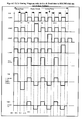
- Figure 1 shows the timing waveforms for a standard LCD display using a quadruplex multiplex method.
- the LCD segment is inactive (OFF) if the RMS voltage is below the LCD threshold voltage and is active (ON) if the LCD RMS voltage is above the threshold voltage.
- the LCD threshold voltage depends on the properties of the liquid used in the LCD and the temperature.
- the optical contrast is defined by the difference in the transparency of an LCD segment that is ON (dark) and an LCD segment that is OFF (transparent). The optical contrast depends on the difference between the RMS voltage in the ON state (Von) and the RMS voltage in the OFF state (Voff). The larger the difference between Von and Voff, the greater is the optical contrast.
- the optical contrast depends as well on the difference between the on-state voltage Von and the LCD threshold voltage. If Von is below or close to the threshold voltage, the LCD is completely or almost transparent. Similarly, if Voff is close or above the threshold voltage, the LCD is completely dark.
- Figures 2 & 3 show the timing diagrams for a similar quadruplex LCD display driven according to this invention.
- Contrast is controlled by tuning the RMS voltage of the LCD segment RMS voltage close to the LCD threshold voltage.
- the RMS voltage calculated above can be controlled by dividing the LCD driving time ( control period) into two parts :
- the LCD driving waveforms are generated by using a software algorithm.
- the segment lines and COM lines are used to drive the LCD.
- Dead time Segment and COM lines are used to control the LCD RMS voltage.
- the LCD RMS voltage is controlled by varying the timing of dead phase as shown in the LCD timing diagram.
- LCD RMS voltage can be adjusted to the optimal value depending up on the operating voltage of the LCD used and the temperature.
- Dead time can be used to decrease Vrms as well as to increase it (on controller with small supply voltage). Dead time is a voltage compensation time to regulate the rms voltage up and down.
- the dead time control technique is independent of LCD multiplexing method (Duplex, Quadruplex%) and bias voltage technique ( 1 ⁇ 2 bias, 1/3 bias). Dead time can be implemented after each "control period" or after each end of frame depending up on quality of the LCD and frequency of the frame to avoid flickering effect on LCD.
- the Controller of LCD pattern + Dead time could be a microcontroller or any kind of ASIC.
- Each frame period consists of four control periods( for quadruplex LCD), one control period per COM line.
- Each COM line generates its waveform during its corresponding control period e.g. COM1 line during (0- T/4).
- COM1 remains at level Vdd/2.
- each control period consists of two parts:
- Vdd voltage Vdd is applied for the segments which have to be turned ON and 0 for the segments which have to be turned OFF.
- COM line which corresponds to this control period is set to low level.
- Other COM lines are set to level Vdd/2.
- all segments and COM lines are inactive(set to low level) if it is desired to decrease the Vrms( figure2) and COM lines are set low, segments lines are set high if is desired to increase the Vrms( figure3).
- Segment Lines are supplied with voltage levels which are inverted to the one applied during OC1.
- COM line which corresponds to this control period is set to high level.
- Other COM lines are set to level Vdd/2.
- Vx 0 ( incase of decrease of rms voltage, figure 2)
- Voff x 1 1 + x V OFF 1 ( for decrease of Vrms)
- Voff x 1+2x 1 + x V OFF 1 (for increase of Vrms)
- Figure 4 shows an implementation of the invention using a standard microcontroller.
- LCD segment RMS voltage is controlled by controlling the timing for the waveforms driving the LCD segment and common lines. These controlled LCD driving waveforms are generated by using software driver.
- An external 2 resistor bridge (per common line) is connected externally to the MCU I/O ports which are used for driving the LCD common lines.
- D.C. power supply of Vdd or Vcc is used for driving all the components of the device.
- the LCD Timing is generated by using the timer interrupts( timer peripheral is available inside the microcontroller).
- Active time starts after timer interrupt1 and dead time starts after timer interrupt2.
- Total 16 interrupts are generated in each frame period with four interrupts per control period. There are four events i.e. OC1, OC2, OC3, OC4 in each control period. Timing for OC1, OC3 are same and then for OC2, OC4 are same.
- the Vdd/2 level is generated by the externally connected resistors.
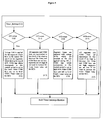
- FIG. 5 shows the flowchart of the software used for the microcomputer implementation of Figure 4,
- Timer interrupt (5.1) triggers an OC1 event (5.2) that applies supply voltage Vdd for segments to be turned on and 0V for segment to be turned off (5.6) while the COM line for the selected period is set to low and other COM lines are tristated.
- the timer is reinitialized.
- event OC2 is triggered (5.3). All segments and COM lines are set to 0V if a Vrms is to be decreased and segment are set high and COM lines low if Vrms is to be increased (5.7). The timer is reinitialized.
- segment lines are supplied levels that are inverted with respect to those supplied during OC1.
- the COM line corresponding to these time slots set high, other COM lines are tristated (5.8).
- the timer is reinitialized.
- the next timer interrupt triggers the OC4 event (5.5). All segment and COM lines are set low if Vrms is to be decreased. COM lines are set high and segments are set low if Vrms is to be increased (5.9). The timer is reinitialized.
Landscapes
- Engineering & Computer Science (AREA)
- Chemical & Material Sciences (AREA)
- Crystallography & Structural Chemistry (AREA)
- Physics & Mathematics (AREA)
- Computer Hardware Design (AREA)
- General Physics & Mathematics (AREA)
- Theoretical Computer Science (AREA)
- Control Of Indicators Other Than Cathode Ray Tubes (AREA)
- Liquid Crystal Display Device Control (AREA)
Abstract
Description
- This invention relates to a Liquid Crystal Display (LCD) driver that provides adjustable contrast independently of the multiplexing method.
- LIQUID CRYSTAL DISPLAYS (LCDs) are used for displaying messages. There are various methods to drive the LCD display. One method uses inbuilt hardware drivers/controllers to control the display of characters/graphics on the LCD. Such LCD modules are easier to interface but are expensive due to the inbuilt hardware drivers/controllers. Another method to drive an LCD display is through a dedicated Microcontroller which has an inbuilt hardware LCD driver to control the LCD display as well as the Contrast. Such a method is also relatively expensive.
- US patent No. 4385294 describes an LCD display controller in which the LCD display is controlled by means of dedicated display drive circuitry. However, this display drive circuitry fails to work if the RMS voltage output of the circuitry is less than the LCD operating voltage. This arrangement is also relatively expensive to use.
- The object of present invention to provide an improved and cost effective system for driving an LCD display and providing adjustable contrast independently of multiplexing requirements..
- Another object of this invention is to provide a solution that makes use of minimal hardware and thus provides a cost effective solution.
- To achieve the said objectives the invention provides an LCD display driver providing adjustable contrast independently of multiplexing requirements, comprising:
- a COM line driver generating as many COM signals as the required multiplexing level, each COM signal being produced in a particular time slot of a repeating signal frame containing multiple time slots, each time slot corresponding to a particular COM signal, and each COM signal containing one or more active periods and one or more inactive periods, the relative time proportions of the active periods and the inactive periods being adjustable, and
- a SEGMENT line driver generating active signals relative to the corresponding time-slot such that the required display segments are turned-on while the remaining display segments are turned off and every LCD segment experiences an AC voltage signal with an essentially zero DC component,
- The required COM and SEGMENT signals are generated at the input-output pins of an ordinary microcontroller using software means.
- The bias voltage is provided by means of a resistor network across the COM signal lines while the COM signals are tristated.
- The RMS voltage level is adjusted to a higher or lower level depending upon the threshold voltage of the LCD display.
- The inactive period is provided in each time slot or at the end of each frame.
- The instant invention also provides a method for driving an LCD display with adjustable contrast independently of multiplexing comprising the steps of:
- generating as many COM signals as the required multiplexing level, each COM signal being produced in a particular time slot of a repeating signal frame containing multiple time slots, each time slot corresponding to a particular COM signal, and each COM signal containing one or more active periods and one or more inactive periods, the relative time proportions of the active periods and the inactive periods being adjustable, and
- supplying active segment signals relative to the corresponding time-slot such that the required display segments are turned-on while the remaining display segments are turned off and every LCD segment experiences an AC voltage signal with an essentially zero like DC component,
- The above method uses a standard microcontroller.
- The biasing voltage is provided by using a resistor network across the COM signal line
- The invention will now be explained with reference to the accompanying drawings:
- Figure 1 shows the basic timing diagrams for a quadruplex multiplexer LCD display.
- Figure 2 shows the timing diagram for a quadruplex LCD display driver according to this invention, in which the LCD voltage is decreased to adapt the RMS output voltage to low threshold voltage LCD display.
- Figure 3 shows the timing diagram for a quadruplex LCD display driver according to this invention, in which the LCD voltage is increased to adapt to high threshold voltage LCD display
- Figure 4 shows an implementation using a standard microcontroller.
- Figure 5 shows a flowchart of the software for the implementation of figure 4.
-
- Figure 1 shows the timing waveforms for a standard LCD display using a quadruplex multiplex method.
- When a low RMS voltage is applied to an LCD, it is practically transparent. The LCD segment is inactive (OFF) if the RMS voltage is below the LCD threshold voltage and is active (ON) if the LCD RMS voltage is above the threshold voltage. The LCD threshold voltage depends on the properties of the liquid used in the LCD and the temperature. The optical contrast is defined by the difference in the transparency of an LCD segment that is ON (dark) and an LCD segment that is OFF (transparent). The optical contrast depends on the difference between the RMS voltage in the ON state (Von) and the RMS voltage in the OFF state (Voff). The larger the difference between Von and Voff, the greater is the optical contrast. The optical contrast depends as well on the difference between the on-state voltage Von and the LCD threshold voltage. If Von is below or close to the threshold voltage, the LCD is completely or almost transparent. Similarly, if Voff is close or above the threshold voltage, the LCD is completely dark.
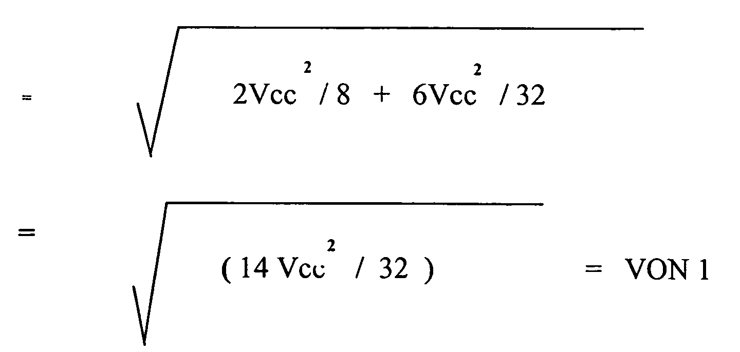
- To turn ON an LCD segment, there should be a voltage difference between the segment and common lines. With reference to the figure 1 that describes the general method to drive the Quadruplex LCD glass( four common lines), the Vrms( On) and Vrms( Off) of an LCD segment is calculated as -


- Figures 2 & 3 show the timing diagrams for a similar quadruplex LCD display driven according to this invention.
- Contrast is controlled by tuning the RMS voltage of the LCD segment RMS voltage close to the LCD threshold voltage.The RMS voltage calculated above can be controlled by dividing the LCD driving time ( control period) into two parts :
- 1. Active Time
- 2. Dead Time
-
- The LCD driving waveforms are generated by using a software algorithm. During the Active time, the segment lines and COM lines are used to drive the LCD. During Dead time Segment and COM lines are used to control the LCD RMS voltage. The LCD RMS voltage is controlled by varying the timing of dead phase as shown in the LCD timing diagram. Thus, LCD RMS voltage can be adjusted to the optimal value depending up on the operating voltage of the LCD used and the temperature.
- Dead time can be used to decrease Vrms as well as to increase it (on controller with small supply voltage). Dead time is a voltage compensation time to regulate the rms voltage up and down. The dead time control technique is independent of LCD multiplexing method (Duplex, Quadruplex...) and bias voltage technique ( ½ bias, 1/3 bias...). Dead time can be implemented after each "control period" or after each end of frame depending up on quality of the LCD and frequency of the frame to avoid flickering effect on LCD. The Controller of LCD pattern + Dead time could be a microcontroller or any kind of ASIC.
- Each frame period consists of four control periods( for quadruplex LCD), one control period per COM line. Each COM line generates its waveform during its corresponding control period e.g. COM1 line during (0- T/4). During other control periods COM1 remains at level Vdd/2. As mentioned above, each control period consists of two parts:
- 1. Active time
- 2. Dead time
-
- During OC1, voltage Vdd is applied for the segments which have to be turned ON and 0 for the segments which have to be turned OFF. COM line which corresponds to this control period is set to low level. Other COM lines are set to level Vdd/2.
- During OC2, all segments and COM lines are inactive(set to low level) if it is desired to decrease the Vrms( figure2) and COM lines are set low, segments lines are set high if is desired to increase the Vrms( figure3).
- During OC3, Segment Lines are supplied with voltage levels which are inverted to the one applied during OC1. COM line which corresponds to this control period is set to high level. Other COM lines are set to level Vdd/2.
- During OC4, all segments and COM lines are inactive(set to low level) if it is desired to decrease the Vrms and COM lines are set high, segments are set low if it is desired to increase the Vrms( figure3).
T = Active Time
xT = Dead Time
x is a proportion of the dead time
Vx = Segment Voltage during the dead timeSince Vx = 0 ( incase of decrease of Rms Voltage, figure 2)
Putting Vx = 0, in the above equation. - In case of increase ofRms voltage , Vx = 0 for 3 dead periods and Vx = +/- Vdd for 5 dead periods( figure 3).
- Putting the value for Vx ,
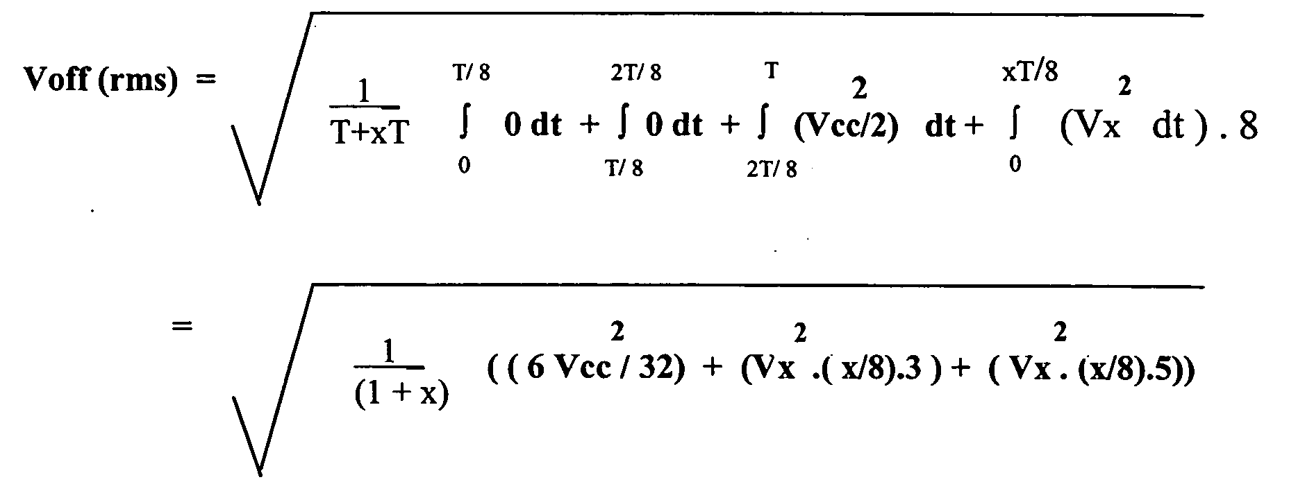
- Since Vx = 0 ( incase of decrease of rms voltage, figure 2)
- In case of increase ofRms voltage, Vx = 0 for 5 dead periods and Vx = +/- Vcc for 3 dead periods (figure 3). Putting the value for Vx ,
- Figure 4 shows an implementation of the invention using a standard microcontroller.
- LCD segment RMS voltage is controlled by controlling the timing for the waveforms driving the LCD segment and common lines. These controlled LCD driving waveforms are generated by using software driver.
- An external 2 resistor bridge (per common line) is connected externally to the MCU I/O ports which are used for driving the LCD common lines. D.C. power supply of Vdd or Vcc is used for driving all the components of the device.
- The LCD Timing is generated by using the timer interrupts( timer peripheral is available inside the microcontroller).
- Active time starts after timer interrupt1 and dead time starts after timer interrupt2. Total 16 interrupts are generated in each frame period with four interrupts per control period. There are four events i.e. OC1, OC2, OC3, OC4 in each control period. Timing for OC1, OC3 are same and then for OC2, OC4 are same.
- The Vdd/2 level is generated by the externally connected resistors.
- Figure 5 shows the flowchart of the software used for the microcomputer implementation of Figure 4, Timer interrupt (5.1) triggers an OC1 event (5.2) that applies supply voltage Vdd for segments to be turned on and 0V for segment to be turned off (5.6) while the COM line for the selected period is set to low and other COM lines are tristated. The timer is reinitialized.
- At the next timer interrupt (5.1) event OC2 is triggered (5.3). All segments and COM lines are set to 0V if a Vrms is to be decreased and segment are set high and COM lines low if Vrms is to be increased (5.7). The timer is reinitialized.
- At the next timer interrupt event OC3 is triggered (5.4). Segment lines are supplied levels that are inverted with respect to those supplied during OC1. The COM line corresponding to these time slots set high, other COM lines are tristated (5.8). The timer is reinitialized.
- The next timer interrupt triggers the OC4 event (5.5). All segment and COM lines are set low if Vrms is to be decreased. COM lines are set high and segments are set low if Vrms is to be increased (5.9). The timer is reinitialized.
- The entire sequence is repeated continuously.
Claims (10)
- An LCD display driver providing adjustable contrast independently of multiplexing requirements, comprising:with the logic level of the SEGMENT signals and the relative active time to inactive time for the SEGMENT & COM being adjustable to increase or decrease the RMS voltage level across the LCD elements as desired.a COM line driver generating as many COM signals as the required multiplexing level, each COM signal being produced in a particular time slot of a repeating signal frame containing multiple time slots, each time slot corresponding to a particular COM signal, and each COM signal containing one or more active periods and one or more inactive periods, the relative time proportions of the active periods and the inactive periods being adjustable, anda SEGMENT line driver generating active signals relative to the corresponding time-slot such that the required display segments are turned-on while the remaining display segments are turned off and every LCD segment experiences an AC voltage signal with an essentially zero DC component,
- An LCD driver as claimed in claim 1, wherein the required COM and SEGMENT signals are generated at the input-output pins of an ordinary microcontroller using software means.
- An LCD driver as claimed in claim 1, wherein the bias voltage is provided by means of a resistor network across the COM signal lines while the COM signals are tristated.
- An LCD driver as claimed in claim 1 wherein the RMS voltage level is adjusted to a higher or lower level depending upon the threshold voltage of the LCD display.
- An LCD driver as claimed in claim 1 wherein the LCD driver is implemented as an ASIC
- An LCD driver as claimed in claim 1 wherein the inactive period is provided in each time slot.
- An LCD driver as claimed in claim 1 wherein the inactive period is provided at the end of each frame.
- A method for driving an LCD display with adjustable contrast independently of multiplexing requirements comprising the steps of :with the logic level of the SEGMENT signals and the relative active time to inactive time for the SEGMENT & COM being adjustable to increase or decrease the RMS voltage level across the LCD elements as desired.generating as many COM signals as the required multiplexing level, each COM signal being produced in a particular time slot of a repeating signal frame containing multiple time slots, each time slot corresponding to a particular COM signal, and each COM signal containing one or more active periods and one or more inactive periods, the relative time proportions of the active periods and the inactive periods being adjustable, andsupplying active segment signals relative to the corresponding time-slot such that the required display segments are turned-on while the remaining display segments are turned off and every LCD segment experiences an AC voltage signal with an essentially zero like DC component,
- A method as claimed in claim 8 using a standard microcontroller.
- A method as claimed in claim 8 wherein the biasing voltage is provided by using a resistor network across the COM signal line.
Applications Claiming Priority (2)
| Application Number | Priority Date | Filing Date | Title |
|---|---|---|---|
| IN1505DE2003 | 2003-12-02 | ||
| INDE15052003 | 2003-12-02 |
Publications (3)
| Publication Number | Publication Date |
|---|---|
| EP1538596A2 true EP1538596A2 (en) | 2005-06-08 |
| EP1538596A3 EP1538596A3 (en) | 2008-07-09 |
| EP1538596B1 EP1538596B1 (en) | 2013-07-17 |
Family
ID=34452220
Family Applications (1)
| Application Number | Title | Priority Date | Filing Date |
|---|---|---|---|
| EP04028541.3A Expired - Lifetime EP1538596B1 (en) | 2003-12-02 | 2004-12-02 | LCD driver with adjustable contrast |
Country Status (2)
| Country | Link |
|---|---|
| US (1) | US7388565B2 (en) |
| EP (1) | EP1538596B1 (en) |
Cited By (2)
| Publication number | Priority date | Publication date | Assignee | Title |
|---|---|---|---|---|
| WO2006122097A2 (en) | 2005-05-09 | 2006-11-16 | Texas Instruments Incorporated | Data-dependent, logic-level drive scheme for driving lcd panels |
| CN103854623A (en) * | 2014-03-11 | 2014-06-11 | 亚世光电股份有限公司 | Segmented multi-path liquid crystal display achieving driving by I/O port of MCU and method |
Families Citing this family (5)
| Publication number | Priority date | Publication date | Assignee | Title |
|---|---|---|---|---|
| US8885139B2 (en) * | 2005-01-21 | 2014-11-11 | Johnson & Johnson Vision Care | Adaptive electro-active lens with variable focal length |
| EP1875454B1 (en) * | 2005-04-27 | 2014-06-11 | Semtech Corporation | Circuit and method for controlling a liquid crystal segment display |
| BRPI0713005A2 (en) * | 2006-06-12 | 2012-04-17 | Johnson & Johnson Vision Care | method for reducing power consumption with electro-optical lenses |
| US8115717B2 (en) * | 2007-06-19 | 2012-02-14 | Raman Research Institute | Method and system for line by line addressing of RMS responding display matrix with wavelets |
| CN106782257B (en) * | 2015-11-20 | 2020-03-17 | 晶门科技有限公司 | Apparatus and method for driving electronic paper display |
Citations (1)
| Publication number | Priority date | Publication date | Assignee | Title |
|---|---|---|---|---|
| US4385294A (en) | 1978-10-05 | 1983-05-24 | Texas Instruments Incorporated | RMS Voltage control with variable duty cycle for matching different liquid crystal display materials |
Family Cites Families (12)
| Publication number | Priority date | Publication date | Assignee | Title |
|---|---|---|---|---|
| JPS59176985A (en) * | 1983-03-26 | 1984-10-06 | Citizen Watch Co Ltd | Liquid crystal television receiver |
| US5596554A (en) * | 1993-06-04 | 1997-01-21 | Hagadorn; Hubert W. | Set operation in a timepiece having an electrooptical display |
| US6127994A (en) * | 1997-04-30 | 2000-10-03 | Motorola, Inc. | Method for multiplex driving a passive liquid crystal display (LCD) using modulated pulse widths |
| US6069598A (en) * | 1997-08-29 | 2000-05-30 | Candescent Technologies Corporation | Circuit and method for controlling the brightness of an FED device in response to a light sensor |
| WO1999021159A1 (en) * | 1997-10-17 | 1999-04-29 | Motorola Inc. | Method for controlling brightness in a flat panel display |
| US6075509A (en) * | 1997-11-17 | 2000-06-13 | Motorola, Inc. | Integrated multiplex drive system for a passive liquid crystal display (LCD) using modulated pulse widths |
| KR100513910B1 (en) * | 1998-02-23 | 2005-09-13 | 세이코 엡슨 가부시키가이샤 | Method of driving electro-optical device, circuit for driving electro-optical device, electro-optical device, and electronic device |
| EP1325093A2 (en) * | 2000-09-26 | 2003-07-09 | Matsushita Electric Industrial Co., Ltd. | Display unit and drive system thereof and an information display unit |
| KR100823047B1 (en) * | 2000-10-02 | 2008-04-18 | 가부시키가이샤 한도오따이 에네루기 켄큐쇼 | Self-luminescent device and driving method thereof |
| KR100843685B1 (en) * | 2001-12-27 | 2008-07-04 | 엘지디스플레이 주식회사 | Method and apparatus for driving a liquid crystal display |
| US6894668B2 (en) * | 2002-05-03 | 2005-05-17 | Eastman Kodak Company | General 2 voltage levels driving scheme for cholesterical liquid crystal displays |
| EP1418568B1 (en) * | 2002-11-07 | 2007-01-10 | Dialog Semiconductor GmbH | Method and system for saving power in row driver circuits for monochrome liquid crystal displays |
-
2004
- 2004-12-01 US US11/001,656 patent/US7388565B2/en not_active Expired - Fee Related
- 2004-12-02 EP EP04028541.3A patent/EP1538596B1/en not_active Expired - Lifetime
Patent Citations (1)
| Publication number | Priority date | Publication date | Assignee | Title |
|---|---|---|---|---|
| US4385294A (en) | 1978-10-05 | 1983-05-24 | Texas Instruments Incorporated | RMS Voltage control with variable duty cycle for matching different liquid crystal display materials |
Non-Patent Citations (1)
| Title |
|---|
| BURGAN ET AL.: "MOTOROLA TECHNICAL DEVELOPMENTS", vol. 31, June 1997, MOTOROLA, INC., article "Liquid Crystal Display Digital Contrast Adjust", pages: 80 - 83 |
Cited By (4)
| Publication number | Priority date | Publication date | Assignee | Title |
|---|---|---|---|---|
| WO2006122097A2 (en) | 2005-05-09 | 2006-11-16 | Texas Instruments Incorporated | Data-dependent, logic-level drive scheme for driving lcd panels |
| EP1886300A4 (en) * | 2005-05-09 | 2009-10-28 | Texas Instruments Inc | Data-dependent, logic-level drive scheme for driving lcd panels |
| CN103854623A (en) * | 2014-03-11 | 2014-06-11 | 亚世光电股份有限公司 | Segmented multi-path liquid crystal display achieving driving by I/O port of MCU and method |
| CN103854623B (en) * | 2014-03-11 | 2017-01-18 | 亚世光电股份有限公司 | Segmented multi-path liquid crystal display achieving driving by I/O port of MCU and method |
Also Published As
| Publication number | Publication date |
|---|---|
| US20050134530A1 (en) | 2005-06-23 |
| EP1538596B1 (en) | 2013-07-17 |
| EP1538596A3 (en) | 2008-07-09 |
| US7388565B2 (en) | 2008-06-17 |
Similar Documents
| Publication | Publication Date | Title |
|---|---|---|
| KR20080063020A (en) | LCD Display | |
| US6535191B1 (en) | Liquid crystal display device | |
| KR980003691A (en) | Display | |
| KR20030015033A (en) | Power of sequence for apparatus and driving for method thereof | |
| KR20090026577A (en) | Display device and its discharge device | |
| JP5148048B2 (en) | Bistable nematic liquid crystal display device and method for controlling such a device | |
| EP1538596B1 (en) | LCD driver with adjustable contrast | |
| US20080084412A1 (en) | Liquid crystal display device and method for driving the same | |
| US20170011675A1 (en) | Modulator for a mux lcd | |
| KR101231840B1 (en) | Liquid crystal display and method for driving the same | |
| US7474291B2 (en) | Relative brightness adjustment for LCD driver ICs | |
| TW200506445A (en) | Display device | |
| KR100687542B1 (en) | Driving circuit of liquid crystal display | |
| US20110069054A1 (en) | Voltage regulator, voltage regulation method, and liquid crystal display device using the same | |
| US7880704B2 (en) | Energy saving passive matrix display device and method for driving the column voltage having reduced transitions | |
| EP0616311B1 (en) | Matrix display device with two-terminal non-linear elements in series with the pixels and method for driving such | |
| EP0811179B1 (en) | Liquid crystal display device | |
| KR20090073646A (en) | LCD and its driving method | |
| KR20070025662A (en) | LCD and its driving method | |
| KR20010004914A (en) | Liquid Crystal Display multi-driving method | |
| US12512038B2 (en) | Display apparatus | |
| KR101194850B1 (en) | Liquid crystal display and driving method for the same | |
| CN111429855A (en) | Visual angle switching circuit and display device | |
| JP2007047788A (en) | Liquid crystal display | |
| KR100192648B1 (en) | Method for driving DHF liquid crystal cell and DHF liquid crystal cell using same |
Legal Events
| Date | Code | Title | Description |
|---|---|---|---|
| PUAI | Public reference made under article 153(3) epc to a published international application that has entered the european phase |
Free format text: ORIGINAL CODE: 0009012 |
|
| AK | Designated contracting states |
Kind code of ref document: A2 Designated state(s): AT BE BG CH CY CZ DE DK EE ES FI FR GB GR HU IE IS IT LI LT LU MC NL PL PT RO SE SI SK TR |
|
| AX | Request for extension of the european patent |
Extension state: AL BA HR LV MK YU |
|
| PUAL | Search report despatched |
Free format text: ORIGINAL CODE: 0009013 |
|
| AK | Designated contracting states |
Kind code of ref document: A3 Designated state(s): AT BE BG CH CY CZ DE DK EE ES FI FR GB GR HU IE IS IT LI LT LU MC NL PL PT RO SE SI SK TR |
|
| AX | Request for extension of the european patent |
Extension state: AL BA HR LV MK YU |
|
| 17P | Request for examination filed |
Effective date: 20090108 |
|
| AKX | Designation fees paid |
Designated state(s): FR IT |
|
| 17Q | First examination report despatched |
Effective date: 20090319 |
|
| REG | Reference to a national code |
Ref country code: DE Ref legal event code: 8566 |
|
| RAP1 | Party data changed (applicant data changed or rights of an application transferred) |
Owner name: STMICROELECTRONICS PVT. LTD. Owner name: STMICROELECTRONICS GMBH |
|
| GRAP | Despatch of communication of intention to grant a patent |
Free format text: ORIGINAL CODE: EPIDOSNIGR1 |
|
| GRAS | Grant fee paid |
Free format text: ORIGINAL CODE: EPIDOSNIGR3 |
|
| GRAA | (expected) grant |
Free format text: ORIGINAL CODE: 0009210 |
|
| RAP1 | Party data changed (applicant data changed or rights of an application transferred) |
Owner name: STMICROELECTRONICS GMBH Owner name: STMICROELECTRONICS INTERNATIONAL N.V. |
|
| AK | Designated contracting states |
Kind code of ref document: B1 Designated state(s): FR IT |
|
| REG | Reference to a national code |
Ref country code: FR Ref legal event code: CD Owner name: STMICROELECTRONICS APPLICATION GMBH, DE Effective date: 20140127 Ref country code: FR Ref legal event code: CD Owner name: STMICROELECTRONICS INTERNATIONAL N.V., NL Effective date: 20140127 Ref country code: FR Ref legal event code: CA Effective date: 20140127 |
|
| PLBE | No opposition filed within time limit |
Free format text: ORIGINAL CODE: 0009261 |
|
| STAA | Information on the status of an ep patent application or granted ep patent |
Free format text: STATUS: NO OPPOSITION FILED WITHIN TIME LIMIT |
|
| 26N | No opposition filed |
Effective date: 20140422 |
|
| REG | Reference to a national code |
Ref country code: FR Ref legal event code: PLFP Year of fee payment: 12 |
|
| REG | Reference to a national code |
Ref country code: FR Ref legal event code: PLFP Year of fee payment: 13 |
|
| REG | Reference to a national code |
Ref country code: FR Ref legal event code: PLFP Year of fee payment: 14 |
|
| PGFP | Annual fee paid to national office [announced via postgrant information from national office to epo] |
Ref country code: IT Payment date: 20181122 Year of fee payment: 15 Ref country code: FR Payment date: 20181127 Year of fee payment: 15 |
|
| PG25 | Lapsed in a contracting state [announced via postgrant information from national office to epo] |
Ref country code: FR Free format text: LAPSE BECAUSE OF NON-PAYMENT OF DUE FEES Effective date: 20191231 Ref country code: IT Free format text: LAPSE BECAUSE OF NON-PAYMENT OF DUE FEES Effective date: 20191202 |