EP1537626B1 - Compact dual band circular pifa - Google Patents
Compact dual band circular pifa Download PDFInfo
- Publication number
- EP1537626B1 EP1537626B1 EP03737126A EP03737126A EP1537626B1 EP 1537626 B1 EP1537626 B1 EP 1537626B1 EP 03737126 A EP03737126 A EP 03737126A EP 03737126 A EP03737126 A EP 03737126A EP 1537626 B1 EP1537626 B1 EP 1537626B1
- Authority
- EP
- European Patent Office
- Prior art keywords
- radiating element
- ground plane
- antenna
- feed
- pifa
- Prior art date
- Legal status (The legal status is an assumption and is not a legal conclusion. Google has not performed a legal analysis and makes no representation as to the accuracy of the status listed.)
- Expired - Lifetime
Links
- 230000009977 dual effect Effects 0.000 title abstract description 21
- 239000000758 substrate Substances 0.000 claims description 8
- MTAZNLWOLGHBHU-UHFFFAOYSA-N butadiene-styrene rubber Chemical compound C=CC=C.C=CC1=CC=CC=C1 MTAZNLWOLGHBHU-UHFFFAOYSA-N 0.000 claims description 2
- 229920001903 high density polyethylene Polymers 0.000 claims description 2
- 239000004700 high-density polyethylene Substances 0.000 claims description 2
- 239000004417 polycarbonate Substances 0.000 claims description 2
- 229920000515 polycarbonate Polymers 0.000 claims description 2
- 230000002093 peripheral effect Effects 0.000 claims 3
- 229940063583 high-density polyethylene Drugs 0.000 claims 1
- 238000005192 partition Methods 0.000 abstract description 5
- 230000010354 integration Effects 0.000 abstract description 2
- PEZNEXFPRSOYPL-UHFFFAOYSA-N (bis(trifluoroacetoxy)iodo)benzene Chemical compound FC(F)(F)C(=O)OI(OC(=O)C(F)(F)F)C1=CC=CC=C1 PEZNEXFPRSOYPL-UHFFFAOYSA-N 0.000 abstract 3
- 229910000679 solder Inorganic materials 0.000 description 17
- 239000004020 conductor Substances 0.000 description 10
- XVIZMMSINIOIQP-UHFFFAOYSA-N 1,2-dichloro-3-(2-chlorophenyl)benzene Chemical compound ClC1=CC=CC(C=2C(=CC=CC=2)Cl)=C1Cl XVIZMMSINIOIQP-UHFFFAOYSA-N 0.000 description 8
- GXVMAQACUOSFJF-UHFFFAOYSA-N 1,3-dichloro-5-(2-chlorophenyl)benzene Chemical compound ClC1=CC(Cl)=CC(C=2C(=CC=CC=2)Cl)=C1 GXVMAQACUOSFJF-UHFFFAOYSA-N 0.000 description 7
- PXAGFNRKXSYIHU-UHFFFAOYSA-N 1,3-dichloro-2-(2,6-dichlorophenyl)benzene Chemical compound ClC1=CC=CC(Cl)=C1C1=C(Cl)C=CC=C1Cl PXAGFNRKXSYIHU-UHFFFAOYSA-N 0.000 description 5
- 238000005476 soldering Methods 0.000 description 5
- 230000000694 effects Effects 0.000 description 4
- 238000005516 engineering process Methods 0.000 description 4
- 230000003287 optical effect Effects 0.000 description 4
- 238000004891 communication Methods 0.000 description 3
- 230000005855 radiation Effects 0.000 description 3
- 239000003989 dielectric material Substances 0.000 description 2
- 230000010287 polarization Effects 0.000 description 2
- 230000006978 adaptation Effects 0.000 description 1
- 238000013459 approach Methods 0.000 description 1
- 230000010267 cellular communication Effects 0.000 description 1
- -1 for example Substances 0.000 description 1
- 239000002184 metal Substances 0.000 description 1
- 238000005457 optimization Methods 0.000 description 1
- 230000035945 sensitivity Effects 0.000 description 1
- 238000000926 separation method Methods 0.000 description 1
- 238000005549 size reduction Methods 0.000 description 1
Images


Classifications
-
- H—ELECTRICITY
- H01—ELECTRIC ELEMENTS
- H01Q—ANTENNAS, i.e. RADIO AERIALS
- H01Q1/00—Details of, or arrangements associated with, antennas
- H01Q1/12—Supports; Mounting means
- H01Q1/22—Supports; Mounting means by structural association with other equipment or articles
- H01Q1/24—Supports; Mounting means by structural association with other equipment or articles with receiving set
- H01Q1/241—Supports; Mounting means by structural association with other equipment or articles with receiving set used in mobile communications, e.g. GSM
-
- H—ELECTRICITY
- H01—ELECTRIC ELEMENTS
- H01Q—ANTENNAS, i.e. RADIO AERIALS
- H01Q5/00—Arrangements for simultaneous operation of antennas on two or more different wavebands, e.g. dual-band or multi-band arrangements
- H01Q5/30—Arrangements for providing operation on different wavebands
- H01Q5/307—Individual or coupled radiating elements, each element being fed in an unspecified way
- H01Q5/342—Individual or coupled radiating elements, each element being fed in an unspecified way for different propagation modes
- H01Q5/357—Individual or coupled radiating elements, each element being fed in an unspecified way for different propagation modes using a single feed point
- H01Q5/364—Creating multiple current paths
- H01Q5/371—Branching current paths
-
- H—ELECTRICITY
- H01—ELECTRIC ELEMENTS
- H01Q—ANTENNAS, i.e. RADIO AERIALS
- H01Q9/00—Electrically-short antennas having dimensions not more than twice the operating wavelength and consisting of conductive active radiating elements
- H01Q9/04—Resonant antennas
- H01Q9/0407—Substantially flat resonant element parallel to ground plane, e.g. patch antenna
- H01Q9/0421—Substantially flat resonant element parallel to ground plane, e.g. patch antenna with a shorting wall or a shorting pin at one end of the element
-
- H—ELECTRICITY
- H01—ELECTRIC ELEMENTS
- H01Q—ANTENNAS, i.e. RADIO AERIALS
- H01Q9/00—Electrically-short antennas having dimensions not more than twice the operating wavelength and consisting of conductive active radiating elements
- H01Q9/04—Resonant antennas
- H01Q9/0407—Substantially flat resonant element parallel to ground plane, e.g. patch antenna
- H01Q9/0442—Substantially flat resonant element parallel to ground plane, e.g. patch antenna with particular tuning means
Definitions
- the present invention relates to Planar Inverted F-Antenna (PIFA), and more particularly, PIFA antenna with non-conventional shapes and an integrated feed line on a ground plane.
- PIFA Planar Inverted F-Antenna
- dual ISM band operation can be accomplished using either external or internal antennas.
- External antennas are large and susceptible to mechanical damage.
- internal antennas are unseen by the user, smaller, and less susceptible to mechanical damage.
- internal antenna are constrained in effectiveness because of the size and volume restrictions associated with wireless devices.
- EP 1 020 947 discloses an antenna body part using a separate metal shield as ground plane.
- US 2001/0033250 discloses an asymmetrical dipole antenna.
- Tarvas et al discloses a quarter-wave planar inverted F-type antenna.
- US 2002/0033772 discloses an antenna device for a portable radio communication device having a microstrip line.
- DE 201 14 387 discloses a planar inverted dual- or multi-frequency F antenna.
- EP 1 096 602 discloses a PIFA-type structure having a projection extending from the radiating plane towards the ground plane or vice versa.
- US 6 366 243 discloses a planar antenna having a circular shape.
- Hsu et al reports a dual band microstrip antenna with a circular radiating element using an air-substrate.
- the dual frequency operation of the microstrip antenna of Hsu et al is realized through two separate linear slots. The two slots are placed symmetrically with respect to the central axis of the radiating element. The axis of the microstrip feed line is also parallel to the axes of the slots.
- a dual frequency circular microstrip antenna with a pair of are-shaped slots has been studied in Kin-Lu Wong and Gui-Biu Hsieh, "Dual-Frequency Circular Microstrip Antenna with a Pair of Arc-Shaped Slots", MICROWAVE AND OPTICAL TECHNOLOGY LETTERS, Vol. 19, No- 6, December 20 1998, pp.410-412 (hereinafter referred to as Wong et al).
- the two arc-shaped slots are located on either side of one of the central axes. In the work of Wong et al, the two arc-shaped slots are also symmetrically placed with respect to the referred central axis of the antenna.
- the size of the radiating element corresponds to half wavelength at the center frequency of the lower resonant band.
- Circular patch antennas also provide some insight into the present invention.
- the case studies of circular patches with a single arc or U-shaped slot are described in the work of K.M. Luk, Y.W. Lee, K.F. Tong, and K.F.Lee, "Experimental studies of circular patches with slots", IBE Proc.-Microw. Antennas Propagation, Vol. 144, No. 6, Dec. 1997, pp. 421-424 (hereinafter referred to as Luk et al).
- Luk et al With a single arc shaped slot, the choice of center or offset feed determines the dual or single frequency operation.
- the choice of a U-shaped slot, as in the paper of Luk et al results only in a single band operation with a wider impedance bandwidth.
- PIFAs have a greater potential. Apart from extensive utility of PIFA in commercial cellular communications, PIFA continues to find its usefulness in many other systems applications such as WLAN, the Internet, or the like.
- the printed circuit board of the communication device serves as the ground plane of the internal antenna.
- the PIFA is characterized by many distinguishing properties such as relative lightweight, ease of adaptation and integration into the device chassis, moderate range of bandwidth, versatile for optimization, and multiple potential approaches for size reduction. Its sensitivity to both the vertical and horizontal polarization is of immense practical importance in wireless devices because of multi path propagation conditions. All these features render the PIFA to be as good a choice as any internal antenna for wireless device applications.
- PIFAs have a unique advantage because it can be fashioned into varieties of either Polarization or pattern Diversity schemes.
- FIG. 9A and 9B A conventional single band PIFA assembly is illustrated in Figures 9A and 9B.
- the PIFA 110 shown in Figure 9A and Figure 9B consists of a radiating element 101, a ground plane 102, a connector feed pin 104a, and a conductive post or pin 107.
- a power feed hole 103 is located in radiation element corresponding to connector feed pin 104a.
- Connector feed pin 104a serves as a feed path for RF power to the radiating element 101.
- Connector feed pin 104a is inserted through the feed hole 103 from the bottom surface of the ground plane 102.
- the connector feed pin 104a is electrically insulated from the ground plane 102 where the pin passes through the hole in the ground plane 102.
- the connector feed pin 104a is electrically connected to the radiating element 101 at point 105a with, for example, solder.
- the body of the feed connector 104b is electrically connected to the ground plane at point 105b with, for example, solder.
- the connector feed pin 104a is electrically insulated from the body of the feed connector 104b.
- a through hole 106 is located in radiation element 101 corresponding to conductive post or pin 107. Conductive post 107 is inserted through the hole 106.
- the conductive post 107 serves as a short circuit between the radiating element 101 and ground plane 102.
- the conductive post 107 is electrically connected to the radiating element 101 at point 108a with, for example, solder.
- the conductive post 107 is also electrically connected to the ground plane 102 at point, 108b with, for example, solder.
- the resonant frequency of the PIFA 110 is determined by the length (L) and width (W) of the radiating element 101 and is slightly affected by the locations of the feed pin 104a and the shorting pin 107.
- the impedance match of the PIFA 110 is achieved by adjusting the diameter of the connector feed pin 104a, by adjusting the diameter of the conductive shorting post 107, and by adjusting the separation distance between the connector feed pin 104a and the conductive shorting post 107.
- the fundamental limitation of the configuration of the PIFA 110 described in Figure 9A and Figure 9B is the requirement of relatively large dimensions of length (L) and width (W) of the radiating element 101 to achieve desired resonant frequency band. This configuration is limited to only single operating frequency band applications. If PIFA was a dual band PIFA, a slot (not shown) would reside in radiating element 101 to quasi partition the radiating element 101.
- FIGS. 9A and 9B the majority of PIFA designs focus on PIFA designs having a rectangular or square shape. Thus, it would be desirous to develop a compact dual ISM band internal PIFA having a non-conventional shapes.
- This invention presents new schemes of designing circular shaped PIFAs with a small ground plane. Deviating distinctly from the routine and conventional feed structure usually employed in PIFA design, this invention also demonstrates that the RF feed line system can be integrated to the PIFAs.
- planar inverted F antennas are disclosed.
- the planar inverted F antennas include non-rectangular radiating elements residing on a dielectric carriage, which in turn resides on a ground plane.
- a slot in the radiating element quasi partitions the radiating element.
- a feed pin, conducting post, and matching stub are used to feed power to the radiating element and tune the PIFA to the appropriate frequency.
- Hsu et al. and Wong et al. describe a microstrip antenna where the size of the radiating element corresponds to half wavelength at the center frequency of the lower resonant band. Unlike the Hus et al. and Wong et al. antennas, however, the present invention uses a single slot to yield dual frequency operation of circular PIFA. Further, because of the shorting post associated with the PIFA, the size of the radiating element of the circular PIFA of this invention corresponds only to quarter wavelength or less at the center frequency of the lower resonant band.
- the present invention uses a U-shaped slot as in Luk et al.
- the circular patch antenna of Luk et al. has single band operation with a wider impedance bandwidth.
- the present invention employs a single slot to exhibit dual frequency operation.
- the dual frequency operation of the circular PIFA has been demonstrated with other slot shapes as well, such as, for example, a single arc shaped slot.
- the dual band operation of the circular PIFA of this invention has been accomplished with a radiating element of quarter wavelength in size corresponding to the mid frequency of the lower band.
- the present invention can use a relatively smaller ground plane, such as, for example ground planes ranging from sizes of 30 to 45 mm(L) by 25 to 30 mm (W) thereby accomplishing the compactness of the overall PIFA structure.
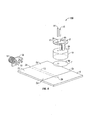
- PIFA 120 illustrative of a first embodiment of the present invention is shown.
- PIFA 120 has a radio frequency (RF) power connector 1, a ground plane 7, a radiating element 8, a dielectric carriage 10, a slot 11, a microstrip feed line 13, and a printed circuit board (PCB) 16.
- PCB 16 has a metallic region 17 and a non-metallic region 18.
- Dielectric carriage 10 could be many types of dielectric material, such as, for example, high density polyethylene, acrolonitrite butadiene styrene, polycarbonates, and the like. Generally, it has been found that dielectric materials with a dielectric contrast in the range of about 2.5 to about 3.5 work well.
- PIFA 120 resides on PCB 16 such that a portion of PIFA 120 is aligned with both metallic (17) and non-metallic (18) regions. PIFA, 120 is shown with a majority of the radiating element existing over non-metallic region 18. It is possible to arrange PIFA 120 so more or less of the radiating element resides over non-metallic region 18. Generally, PIFA 120 works better when more of the radiating element is over non-metallic region 18. In PIFA 120, while the microstrip feed 13 is on the bottom surface of the PCB 16, the metallic region 17 is on the top surface of PCB 16.
- power connector 1 can be any number of equivalent connector, it has been found that a SMA connector is useful.
- the SMA connector has a center conductor 1c and outer conductors 1a and 1b. As shown in FIG. 6, center conductor 1c is attached, such as by soldering, to a first end 2a of microstrip 13. A second end 3a of microstrip 13 is attached, such as by soldering, to a feed pin 14.
- Connector 1 generally also has outer conductors 1a and 1b. Outer conductors 1a and 1b are attached, such as by soldering, to PCB 16, such as at first solder point 5c and second solder point 5d are normally arranged such that they are symmetrical with respect to the central axis of the microstrip feed line 13. The locations of first solder point 5c and second solder point 5d are such that they are symmetrical with respect to the central axis of the microstrip feed line 13.
- ground plane 7 resides on PCB 16 such that the feed via hole in ground plane 7 aligns with second end 3a of microstrip 13. At least third solder point 5a and fourth solder point 5b connect ground plane 7 to PCB 16.
- Radiating element 8 contains slot 11, a conducting post 15, and a matching stub 9.
- Slot 11 is formed on the radiating element 8 by making a trace from a point located on the left hand side of feed pin 14 to a point positioned on the right hand side of conducting post 15. In this case, slot 11 has an arc of about 270 degrees, but the arc could be from about 180 degrees to about 300 degrees depending on the placement of the feed pin and conducting post.
- Conducting post 15 is attached to radiating element 8 and extends through a via hole in dielectric carriage 10. Conducting post 15 is connected to ground plane 7, but not microstrip 13 ( i.e ., conducting post 15 is grounded).
- Matching stub 9 attached to radiating element 8 at 8a also extends along the outer sidewall of the dielectric carriage 10 without attaching to ground plane 7.
- the size, shape and placement of slot 11, feed pin 14, conducting post 15, and matching stub 9 control the operation frequencies of the dual band ISM PIFA.
- controlling the arc radius of slot 11 has a pronounced effect on the upper frequency of PIFA 120.
- the lower frequency is generally tunable by varying the dimensions and placement of the matching stub 9.
- the locations as well as the sizes of the conducting post 15 and feed pin 14 have small effects on resonant frequencies of PIFA 120.
- FIGS 2, 3a and 3b show plots of VSWR and gain of PIFA 120 with a radius of 7.5 mm and height of 7.5 mm.
- the radius and height can vary between 4 to 10 mm for radius and 4 to 8 mm for height. Also, the radius and height do not have to be equal.
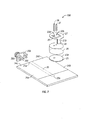
- PIFA 130 illustrative of a second embodiment of the present invention is shown.
- PIFA 130 is similar to PIFA 120, however, PIFA 130 has an alternative slot design.
- the circular PIFA can have many slot configurations and the slots shown in the figures are exemplary and non-limiting.
- PIFA 130 has a connector 38, a microstrip 35, a PCB 34, a ground plane 26, a dielectric carriage 29, a radiating element 27, a slot 30, a feed pin 36, a conducting post 37, a matching stub 28.
- PCB 34 has a metallic region 32 and a non-metallic region 33.
- PIFA 130 resides on PCB 34 such that a portion of PIFA 130 is aligned with both metallic (32) and non metallic (33) regions.
- PIFA 130 is shown with a majority of the radiating element existing over non-metallic region 33. It is possible to arrange PIFA 130 so more or less of the radiating element resides over non-metallic region 33. Generally, PIFA 130 works better when more of the radiating element is over non-metallic region 33.
- a center conductor 20c is attached to a first end 21a of microstrip 35.
- Outer conductors 20a and 20b are attached to PCB 34 at points 24c and 24d.
- a second end 22a of microstrip 35 is attached, such as by soldering, to a feed pin 36.
- Feed pin 36 which extends through via holes in ground plane 26 and dielectric carriage 29 (via holes not specifically labeled but shown in FIG. 7), is connected to radiating element 27 to provide RF power.
- Outer conductors 20a and 20b are attached, such as by soldering, to PCB 34, such as at first solder point 24c and second solder point 24d.
- the locations of solder points 24c and 24d are such that they are symmetrical with respect to the central axis of the microstrip feed line 35.
- ground plane 26 resides on PCB 34 such that the feed via hole in ground plane 26 aligns with second end 22a of microstrip 35. At least third solder point 24a and fourth solder point 24b connect ground plane 26 to PCB 34.
- Radiating element 27 contains slot 30, a conducting post 37, and a matching stub 28.
- Slot 30 is formed on the radiating element 27 such that the contour of the slot is positioned away from the center of the circular PIFA.
- the placement of the U-shaped slot is determined by the positions of feed and shorting posts.
- the length and the width of the U-shaped slot as well as its relative positions with respect to the locations of the feed/shorting posts are determined by the desired frequency tuning.
- the line connecting the feed post and the shorting post is internal to the profile of the U-shaped slot.
- Conducting post 37 is attached to radiating element 27 and extends through a via hole in dielectric carriage 29.
- Conducting post 37 is connected to ground plane 26, but not microstrip 35 (i.e., conducting post 37 is grounded).
- Matching stub 28 attached to radiating element 27 at 27a also extends along the sidewall of the dielectric carriage 29 without attaching to ground plane 26.
- the size, shape and placement of slot 30, feed pin 36, conducting post 37, and matching stub 28 control the operation frequencies of the dual band ISM PIFA. In particular, controlling the placement and size of slot 30 has a pronounced effect on the upper resonant frequency of PIFA 130.
- the lower resonant frequency is generally tunable by varying the dimensions and placement of the matching stub 28.
- the locations as well as sizes of the conducting post 37 and feed pin 36 have small effects on resonant frequencies of PIFA 130.
- the radius and height for PIFA 130 can vary between 4 to 10 mm for radius and 4 to 8 mm for height. Also, the radius and height do not have to be equal.
- PIFA 140 of an example which is useful for understanding of the present invention will be described.
- PIFA 140 is similar to PIFAs 120 and 130. But unlike PIFAs 120 and 130, PIFA 140 eliminates the via holes in the ground plane by strategic locations of the feed pin, shorting post and the choice of the Co Planar Waveguide (CPW) feed line instead of microstrip feed line, as explained below.
- CPW Co Planar Waveguide
- PIFA 140 comprises a connector 56, a PCB 54, CPW 55, a radiating element 47, a dielectric carriage 49, and a ground plane 46.
- PCB 54 contains a metallic region 52 and a non-metallic region 53.
- PIFA 140 resides on non-metallic region 53 of PCB 54.
- the CPW 55 thus, extends from the connector 56 over the metallic region 52 to the interface between the metallic region 52 and non-metallic region 53. It would be possible to arrange PIFA 140 with portions over metallic region 52. But in this configuration, it has been shown that PIFA 140 works better when it resides over the non-metallic portion of PCB 54.
- a center conductor 40c is attached to a first end 41a of CPW 55.
- Outer conductors 40a and 40b of the RF connector 56 are attached to PCB 54 at first solder point 44a and second solder point 44b.
- a second end 42b of CPW 55 is connected to feed strip 42.
- Feed strip 42 extends along the sidewall of the dielectric carriage 49 and is connected to radiating element 47. Because feed strip 42 extends along the sidewall of carriage dielectric 49, the via holes in ground plane 46 and dielectric carriage 49 can be eliminated Similarly, a conducting post 43 is attached to the radiating element 47, extends along the sidewall of the dielectric carriage49, to be attached to ground plane 46.
- a matching stub 48 also attached to radiating element 47 extends along the outer wall of the dielectric carriage 49. The feed strip 42, the conducting post 43 and the matching stub 48 are in flush with the sidewall of the dielectric carriage 49.
- Slot 40 is L-shaped.
- the segment of the L-shaped slot 40 with an opening or gap (open end) in the circumference of the radiating element forms the horizontal section of the L-slot.
- the axis of the horizontal section of the L-slot is perpendicular to the axis of the CPW 55.
- the vertical section of the L-slot 40 has a closed end.
- the axis of the vertical section of the L-slot is parallel to the axis of the CPW 55.
- the size, shape, and placement of slot 40, feed strip 42, conducting post 43, and matching stub 48 control the operation frequencies of the dual ISM band PIFA 140.
- the radius and height for PIFA 140 can vary between 4 to 8 mm for radius and 4 to 8 mm for height. Also, the radius and height do not have to be equal.
Landscapes
- Engineering & Computer Science (AREA)
- Computer Networks & Wireless Communication (AREA)
- Waveguide Aerials (AREA)
- Measuring Pulse, Heart Rate, Blood Pressure Or Blood Flow (AREA)
- External Artificial Organs (AREA)
- Gear-Shifting Mechanisms (AREA)
Abstract
Description
- The present invention relates to Planar Inverted F-Antenna (PIFA), and more particularly, PIFA antenna with non-conventional shapes and an integrated feed line on a ground plane.
- In wireless radio frequency ("RF") data communications there is currently a shift in the requirement from the existing single band operation to dual industrial scientific medical ("ISM") band operation covering, for example, frequency ranges of 2.4-2.5 to 5.15-5.35 GHz. Generally, dual ISM band operation can be accomplished using either external or internal antennas. External antennas are large and susceptible to mechanical damage. Conversely, internal antennas are unseen by the user, smaller, and less susceptible to mechanical damage. However, internal antenna are constrained in effectiveness because of the size and volume restrictions associated with wireless devices.
- In most of the devices, only specified regions with defined volume can accommodate the placement of internal antennas. These regions are usually not of perfect rectangular/square shape or of large size. At times, the available space for internal antennas nearly assumes a circular cylindrical shape of very small area and volume. For optimal performance of the internal antenna, it is desirable that the shape of the radiating structure of the antenna use as much of the allowed area as possible. Dual band ISM internal antenna, however, are generally rectangular in shape, which will be explained in connection with FIG. 9, below. Thus, it would be desirous to develop a non-conventionally shaped PIFA antenna to use more of the available space for internal antenna.
-
EP 1 020 947US 2001/0033250 discloses an asymmetrical dipole antenna. Tarvas et al "An internal dual-band mobile phone antenna" discloses a quarter-wave planar inverted F-type antenna.US 2002/0033772 discloses an antenna device for a portable radio communication device having a microstrip line.DE 201 14 387 discloses a planar inverted dual- or multi-frequency F antenna.EP 1 096 602US 6 366 243 discloses a planar antenna having a circular shape. - There seems to be no work reported on circular shaped either single or dual band PIFAs in open literature. Wen-Hsiu Hsu and Kin-Lu Wong, "A Wideband Circular Patch Antenna", MICROWAVE AND OPTICAL TECHNOLOGY LETTERS, Vol. 25, No. 5, June 5 2000 pp. 328 (hereinafter referred to as Hsu et al) reports a dual band microstrip antenna with a circular radiating element using an air-substrate. The dual frequency operation of the microstrip antenna of Hsu et al is realized through two separate linear slots. The two slots are placed symmetrically with respect to the central axis of the radiating element. The axis of the microstrip feed line is also parallel to the axes of the slots.
- A dual frequency circular microstrip antenna with a pair of are-shaped slots has been studied in Kin-Lu Wong and Gui-Biu Hsieh, "Dual-Frequency Circular Microstrip Antenna with a Pair of Arc-Shaped Slots", MICROWAVE AND OPTICAL TECHNOLOGY LETTERS, Vol. 19, No- 6, December 20 1998, pp.410-412 (hereinafter referred to as Wong et al). The two arc-shaped slots are located on either side of one of the central axes. In the work of Wong et al, the two arc-shaped slots are also symmetrically placed with respect to the referred central axis of the antenna.
- In both of the above research papers, the size of the radiating element corresponds to half wavelength at the center frequency of the lower resonant band.
- Circular patch antennas also provide some insight into the present invention. The case studies of circular patches with a single arc or U-shaped slot are described in the work of K.M. Luk, Y.W. Lee, K.F. Tong, and K.F.Lee, "Experimental studies of circular patches with slots", IBE Proc.-Microw. Antennas Propagation, Vol. 144, No. 6, Dec. 1997, pp. 421-424 (hereinafter referred to as Luk et al). With a single arc shaped slot, the choice of center or offset feed determines the dual or single frequency operation. The choice of a U-shaped slot, as in the paper of Luk et al, results only in a single band operation with a wider impedance bandwidth.
- Recently there has been a drastic increase in the demand for use of internal antennas in wireless applications. In a variety of options for internal antennas, PIFAs seems to have a greater potential. Apart from extensive utility of PIFA in commercial cellular communications, PIFA continues to find its usefulness in many other systems applications such as WLAN, the Internet, or the like. The printed circuit board of the communication device serves as the ground plane of the internal antenna. The PIFA is characterized by many distinguishing properties such as relative lightweight, ease of adaptation and integration into the device chassis, moderate range of bandwidth, versatile for optimization, and multiple potential approaches for size reduction. Its sensitivity to both the vertical and horizontal polarization is of immense practical importance in wireless devices because of multi path propagation conditions. All these features render the PIFA to be as good a choice as any internal antenna for wireless device applications. When it comes to diversity schemes, PIFAs have a unique advantage because it can be fashioned into varieties of either Polarization or pattern Diversity schemes.
- A conventional single band PIFA assembly is illustrated in Figures 9A and 9B. The
PIFA 110 shown in Figure 9A and Figure 9B consists of aradiating element 101, aground plane 102, aconnector feed pin 104a, and a conductive post orpin 107. Apower feed hole 103 is located in radiation element corresponding toconnector feed pin 104a.Connector feed pin 104a serves as a feed path for RF power to the radiatingelement 101.Connector feed pin 104a is inserted through thefeed hole 103 from the bottom surface of theground plane 102. Theconnector feed pin 104a is electrically insulated from theground plane 102 where the pin passes through the hole in theground plane 102. Theconnector feed pin 104a is electrically connected to theradiating element 101 atpoint 105a with, for example, solder. The body of thefeed connector 104b is electrically connected to the ground plane atpoint 105b with, for example, solder. Theconnector feed pin 104a is electrically insulated from the body of thefeed connector 104b. A throughhole 106 is located inradiation element 101 corresponding to conductive post orpin 107.Conductive post 107 is inserted through thehole 106. Theconductive post 107 serves as a short circuit between theradiating element 101 andground plane 102. Theconductive post 107 is electrically connected to theradiating element 101 atpoint 108a with, for example, solder. Theconductive post 107 is also electrically connected to theground plane 102 at point, 108b with, for example, solder. The resonant frequency of thePIFA 110 is determined by the length (L) and width (W) of theradiating element 101 and is slightly affected by the locations of thefeed pin 104a and the shortingpin 107. The impedance match of thePIFA 110 is achieved by adjusting the diameter of theconnector feed pin 104a, by adjusting the diameter of theconductive shorting post 107, and by adjusting the separation distance between theconnector feed pin 104a and theconductive shorting post 107. The fundamental limitation of the configuration of thePIFA 110 described in Figure 9A and Figure 9B is the requirement of relatively large dimensions of length (L) and width (W) of theradiating element 101 to achieve desired resonant frequency band. This configuration is limited to only single operating frequency band applications. If PIFA was a dual band PIFA, a slot (not shown) would reside in radiatingelement 101 to quasi partition theradiating element 101. - As represented by FIGS. 9A and 9B, the majority of PIFA designs focus on PIFA designs having a rectangular or square shape. Thus, it would be desirous to develop a compact dual ISM band internal PIFA having a non-conventional shapes.
- This invention presents new schemes of designing circular shaped PIFAs with a small ground plane. Deviating distinctly from the routine and conventional feed structure usually employed in PIFA design, this invention also demonstrates that the RF feed line system can be integrated to the PIFAs.
- To attain the advantages and in accordance with the purpose of the invention, according to the appended claims, planar inverted F antennas are disclosed. The planar inverted F antennas include non-rectangular radiating elements residing on a dielectric carriage, which in turn resides on a ground plane. A slot in the radiating element quasi partitions the radiating element. A feed pin, conducting post, and matching stub are used to feed power to the radiating element and tune the PIFA to the appropriate frequency.
- The above and other objects and advantages of the present invention will be apparent upon consideration of the following detailed description, taken in conjunction with the accompanying drawings, in which like reference characters refer to like parts throughout, and in which:
- FIG. 1 is perspective view of a planar inverted F antenna illustrative of an embodiment of the present invention;
- FIG. 2 is a frequency-response that depicts the characteristics of a particular PIFA constructed in accordance with an embodiment of the present invention;
- FIGS 3a and 3b are measured radiation patterns of the PIFA associated with Figure 2 for RF frequencies of 2450 and 5250 MHz, respectively.
- FIG. 4 is a perspective view of a planar inverted F antenna illustrative of another embodiment of the present invention;
- FIG. 5 is a perspective view of a planar inverted F antenna which is useful for understanding of the present invention;
- FIG. 6is an exploded view of
PIFA 120 associated with Figure 1; - FIG. 7is an exploded view of
PIFA 130 associated with Figure 4; - FIG. 8 is an exploded view of
PIFA 140 associated with Figure 5; - FIG. 9a is a top view of a prior art single band PIFA; and.
- FIG. 9b is a sectional view the Figure 9a prior art PIFA.
- Embodiments of the present invention are now explained with reference to the drawings. While the present invention is explained with reference to certain shapes, such as "Horse Shoe, U- or L- shaped slot," one of ordinary skill in the art will recognize on reading the disclosure that other shapes are possible, such as "C" shape, elliptical shape, bracket shape, or the like.
- As mentioned above, some prior art designs provide some insight to the present invention. In particular, the following three publications related to prior art antennas are useful: Wen-Hsiu Hsu and Kin-Lu Wong, " A Wideband Circular Patch Antenna", MICROWAVE AND OPTICAL TECHNOLOGY LETTERS, Vol. 25, No. 5, June 5 2000 pp. 328, Kin-Lu Wong and Gui-Bin Hsieh, "Dual-Frequency Circular Microstrip Antenna with a Pair of Arc-Shaped Slots", MICROWAVE AND OPTICAL TECHNOLOGY LETTERS, Vol. 19, No. 6, December 20 1998, pp.410-412, and K.M. Luk, Y.W. Lee, K.F. Tong, and K.F. Lee, "Experimental Studies Of Circular Patches With Slots", IEE Proc.-Microw. Antennas Propagation., Vol. 144, No. 6, Dec. 1997, pp. 421-424. Hsu et al. and Wong et al. describe a microstrip antenna where the size of the radiating element corresponds to half wavelength at the center frequency of the lower resonant band. Unlike the Hus et al. and Wong et al. antennas, however, the present invention uses a single slot to yield dual frequency operation of circular PIFA. Further, because of the shorting post associated with the PIFA, the size of the radiating element of the circular PIFA of this invention corresponds only to quarter wavelength or less at the center frequency of the lower resonant band.
- The present invention uses a U-shaped slot as in Luk et al. However, the circular patch antenna of Luk et al. has single band operation with a wider impedance bandwidth. The present invention employs a single slot to exhibit dual frequency operation. The dual frequency operation of the circular PIFA has been demonstrated with other slot shapes as well, such as, for example, a single arc shaped slot. Further, unlike Luk et al., the dual band operation of the circular PIFA of this invention has been accomplished with a radiating element of quarter wavelength in size corresponding to the mid frequency of the lower band. Finally, the present invention can use a relatively smaller ground plane, such as, for example ground planes ranging from sizes of 30 to 45 mm(L) by 25 to 30 mm (W) thereby accomplishing the compactness of the overall PIFA structure.
- Referring specifically to FIGS. 1 and 6, a
PIFA 120 illustrative of a first embodiment of the present invention is shown.PIFA 120 has a radio frequency (RF)power connector 1, a ground plane 7, a radiatingelement 8, adielectric carriage 10, aslot 11, amicrostrip feed line 13, and a printed circuit board (PCB) 16.PCB 16 has ametallic region 17 and anon-metallic region 18.Dielectric carriage 10 could be many types of dielectric material, such as, for example, high density polyethylene, acrolonitrite butadiene styrene, polycarbonates, and the like. Generally, it has been found that dielectric materials with a dielectric contrast in the range of about 2.5 to about 3.5 work well. Establishing PCB16 with metallic and nonmetallic regions is largely a function of design choice.PIFA 120 resides onPCB 16 such that a portion ofPIFA 120 is aligned with both metallic (17) and non-metallic (18) regions. PIFA, 120 is shown with a majority of the radiating element existing overnon-metallic region 18. It is possible to arrangePIFA 120 so more or less of the radiating element resides overnon-metallic region 18. Generally,PIFA 120 works better when more of the radiating element is overnon-metallic region 18. InPIFA 120, while themicrostrip feed 13 is on the bottom surface of thePCB 16, themetallic region 17 is on the top surface ofPCB 16. - While
power connector 1 can be any number of equivalent connector, it has been found that a SMA connector is useful. The SMA connector has a center conductor 1c andouter conductors first end 2a ofmicrostrip 13. A second end 3a ofmicrostrip 13 is attached, such as by soldering, to afeed pin 14.Feed pin 14, which extends through via holes in ground plane 7 and dielectric carriage 10 (via holes not specifically labeled but shown in FIG. 6), is connected to radiatingelement 8 to provide RF power. -
Connector 1 generally also hasouter conductors Outer conductors PCB 16, such as at first solder point 5c andsecond solder point 5d are normally arranged such that they are symmetrical with respect to the central axis of themicrostrip feed line 13. The locations of first solder point 5c andsecond solder point 5d are such that they are symmetrical with respect to the central axis of themicrostrip feed line 13. - As best seen in FIG. 6, and describing from
PCB 16 to radiatingelement 8, ground plane 7 resides onPCB 16 such that the feed via hole in ground plane 7 aligns with second end 3a ofmicrostrip 13. At leastthird solder point 5a andfourth solder point 5b connect ground plane 7 toPCB 16. -
Radiating element 8 containsslot 11, a conductingpost 15, and a matchingstub 9.Slot 11, which is a horse-shoe shaped slot, can be located in a number of locations to quasipartition radiating element 8.Slot 11 is formed on theradiating element 8 by making a trace from a point located on the left hand side offeed pin 14 to a point positioned on the right hand side of conductingpost 15. In this case,slot 11 has an arc of about 270 degrees, but the arc could be from about 180 degrees to about 300 degrees depending on the placement of the feed pin and conducting post. Conductingpost 15 is attached to radiatingelement 8 and extends through a via hole indielectric carriage 10. Conductingpost 15 is connected to ground plane 7, but not microstrip 13 (i.e., conductingpost 15 is grounded).Matching stub 9 attached to radiatingelement 8 at 8a also extends along the outer sidewall of thedielectric carriage 10 without attaching to ground plane 7. As one of skill in the art would recognize on reading the disclosure, the size, shape and placement ofslot 11,feed pin 14, conductingpost 15, and matchingstub 9 control the operation frequencies of the dual band ISM PIFA. In particular, controlling the arc radius of slot 11 (more or less arc radius) has a pronounced effect on the upper frequency ofPIFA 120. The lower frequency is generally tunable by varying the dimensions and placement of the matchingstub 9. The locations as well as the sizes of the conductingpost 15 andfeed pin 14 have small effects on resonant frequencies ofPIFA 120. FIGS 2, 3a and 3b show plots of VSWR and gain ofPIFA 120 with a radius of 7.5 mm and height of 7.5 mm. The radius and height can vary between 4 to 10 mm for radius and 4 to 8 mm for height. Also, the radius and height do not have to be equal. - Referring to FIGs. 4 and 7, a
PIFA 130 illustrative of a second embodiment of the present invention is shown.PIFA 130 is similar toPIFA 120, however,PIFA 130 has an alternative slot design. As one of skill in the art would recognize on reading this disclosure, the circular PIFA can have many slot configurations and the slots shown in the figures are exemplary and non-limiting. - In particular,
PIFA 130 has aconnector 38, amicrostrip 35, aPCB 34, aground plane 26, adielectric carriage 29, a radiatingelement 27, aslot 30, afeed pin 36, a conductingpost 37, a matchingstub 28.PCB 34 has ametallic region 32 and anon-metallic region 33.PIFA 130 resides onPCB 34 such that a portion ofPIFA 130 is aligned with both metallic (32) and non metallic (33) regions.PIFA 130 is shown with a majority of the radiating element existing overnon-metallic region 33. It is possible to arrangePIFA 130 so more or less of the radiating element resides overnon-metallic region 33. Generally,PIFA 130 works better when more of the radiating element is overnon-metallic region 33. - Referring to FIG. 7, and using an exemplary SMA connector for
power connector 38, a center conductor 20c is attached to afirst end 21a ofmicrostrip 35.Outer conductors PCB 34 atpoints 24c and 24d. Asecond end 22a ofmicrostrip 35 is attached, such as by soldering, to afeed pin 36.Feed pin 36, which extends through via holes inground plane 26 and dielectric carriage 29 (via holes not specifically labeled but shown in FIG. 7), is connected to radiatingelement 27 to provide RF power. -
Outer conductors PCB 34, such as at first solder point 24c andsecond solder point 24d. The locations ofsolder points 24c and 24d are such that they are symmetrical with respect to the central axis of themicrostrip feed line 35. - As best seen in FIG. 7,
ground plane 26 resides onPCB 34 such that the feed via hole inground plane 26 aligns withsecond end 22a ofmicrostrip 35. At leastthird solder point 24a andfourth solder point 24b connectground plane 26 toPCB 34. - Radiating
element 27 containsslot 30, a conductingpost 37, and a matchingstub 28.Slot 30, which in this case is a is a "U" or bracket shaped slot, can be located in a number of locations to quasipartition radiating element 27.Slot 30 is formed on the radiatingelement 27 such that the contour of the slot is positioned away from the center of the circular PIFA. The placement of the U-shaped slot is determined by the positions of feed and shorting posts. The length and the width of the U-shaped slot as well as its relative positions with respect to the locations of the feed/shorting posts are determined by the desired frequency tuning. In the embodiment shown, the line connecting the feed post and the shorting post is internal to the profile of the U-shaped slot. Conductingpost 37 is attached to radiatingelement 27 and extends through a via hole indielectric carriage 29. Conductingpost 37 is connected to groundplane 26, but not microstrip 35 (i.e., conductingpost 37 is grounded).Matching stub 28 attached to radiatingelement 27 at 27a also extends along the sidewall of thedielectric carriage 29 without attaching toground plane 26. As one of skill in the art would recognize on reading the disclosure, the size, shape and placement ofslot 30,feed pin 36, conductingpost 37, and matchingstub 28 control the operation frequencies of the dual band ISM PIFA. In particular, controlling the placement and size ofslot 30 has a pronounced effect on the upper resonant frequency ofPIFA 130. The lower resonant frequency is generally tunable by varying the dimensions and placement of the matchingstub 28. The locations as well as sizes of the conductingpost 37 andfeed pin 36 have small effects on resonant frequencies ofPIFA 130. The radius and height forPIFA 130 can vary between 4 to 10 mm for radius and 4 to 8 mm for height. Also, the radius and height do not have to be equal. - Referring now to FIGS. 5 and 8,
PIFA 140 of an example which is useful for understanding of the present invention will be described.PIFA 140 is similar to PIFAs 120 and 130. But unlike PIFAs 120 and 130,PIFA 140 eliminates the via holes in the ground plane by strategic locations of the feed pin, shorting post and the choice of the Co Planar Waveguide (CPW) feed line instead of microstrip feed line, as explained below. -
PIFA 140 comprises aconnector 56, aPCB 54,CPW 55, a radiatingelement 47, adielectric carriage 49, and aground plane 46.PCB 54 contains ametallic region 52 and anon-metallic region 53. In this example,PIFA 140 resides onnon-metallic region 53 ofPCB 54. TheCPW 55, thus, extends from theconnector 56 over themetallic region 52 to the interface between themetallic region 52 andnon-metallic region 53. It would be possible to arrangePIFA 140 with portions overmetallic region 52. But in this configuration, it has been shown thatPIFA 140 works better when it resides over the non-metallic portion ofPCB 54. - As shown best in FIG. 8, and again using the standard SMA connector for
connector 56, acenter conductor 40c is attached to afirst end 41a ofCPW 55.Outer conductors RF connector 56 are attached toPCB 54 atfirst solder point 44a andsecond solder point 44b. Asecond end 42b ofCPW 55 is connected to feedstrip 42.Feed strip 42 extends along the sidewall of thedielectric carriage 49 and is connected to radiatingelement 47. Becausefeed strip 42 extends along the sidewall ofcarriage dielectric 49, the via holes inground plane 46 anddielectric carriage 49 can be eliminated Similarly, a conductingpost 43 is attached to the radiatingelement 47, extends along the sidewall of the dielectric carriage49, to be attached toground plane 46. A matchingstub 48 also attached to radiatingelement 47 extends along the outer wall of thedielectric carriage 49. Thefeed strip 42, the conductingpost 43 and the matchingstub 48 are in flush with the sidewall of thedielectric carriage 49. -
Slot 40 is L-shaped. The segment of the L-shapedslot 40 with an opening or gap (open end) in the circumference of the radiating element forms the horizontal section of the L-slot. The axis of the horizontal section of the L-slot is perpendicular to the axis of theCPW 55. The vertical section of the L-slot 40 has a closed end. The axis of the vertical section of the L-slot is parallel to the axis of theCPW 55. As one of skill in the art would recognize on reading the disclosure, the size, shape, and placement ofslot 40,feed strip 42, conductingpost 43, and matchingstub 48 control the operation frequencies of the dualISM band PIFA 140. The radius and height forPIFA 140 can vary between 4 to 8 mm for radius and 4 to 8 mm for height. Also, the radius and height do not have to be equal. - While the invention has been particularly shown and described with reference to embodiments thereof, it will be understood by those of ordinary skill in the art that various other changes in the form and details may be made without departing from the scope of the invention. Further, while particular configurations of the present invention have been illustrated and described, other configurations are possible.
Claims (11)
- A plantar inverted F antennas (120; 130; 140) comprising:a circular radiating element (8; 27; 47) comprising an internal side, an external side, and a peripheral edge;a dielectric carriage (10; 27; 47) comprising a radiating side, a ground side, and at least one sidewall;the circular radiating element (8; 27; 47) resides on the dielectric carriage (10; 27; 47) such that the internal side of the radiating element resides closer to the radiating side of the dielectric carriage than the external side;a ground plane (7; 26; 46) comprising a feed side and a carriage side;the dielectric carriage (10; 27; 47) resides on the ground plane (7; 26; 46) such that the carriage side of the ground plane resides closer to the ground side of the dielectric carriage than the feed side;a slot (11; 30; 40);the slot resides in the radiating element;a feed pin (14; 36);a dielectric carriage feed pin via hole;a ground plane feed pin via hole;a conducting post (15; 37);a dielectric carriage conducting post via hole;the conducting post extends from the internal side of the radiating element to the carriage side of the ground plane through the dielectric carriage conducting post via hole and is attached to the carriage side of the ground plane;characterized by
the feed pin attached to the internal side of the radiating element proximate the center of the radiating element;
the feed pin extends from the internal side of the radiating element through the dielectric carriage feed pin via hole and the ground plane feed pin via hole and is adapted to attach to a Microstrip feed line;
the conducting post attached to the internal side of the radiating element proximate the centre of the radiating element;
a matching stub (9; 28; 48);
the matching stub attached to the peripheral edge of the radiating element; and
the matching stub has an extension towards the ground plane from the peripheral edge of the radiating element and the matching stub not touching the ground plane;
the matching stub is in flush with the sidewall of the dielectric carriage. - The antenna of 1, further comprising:a microstrip feed;a substrate;the microstrip feed comprises a ground plane side and a substrate side;the microstrip feed line extends over the substrate towards the ground plane such that the substrate side of the microstrip feed resides closer to the substrate than the ground plane side and the ground plane side resides closer to the ground plane than the substrate side; andthe microstrip feed line is attached to the feed pin at a point aligned with the ground plane feed pin via hole.
- The antenna of claim 2, wherein the substrate comprises a printed circuit board having a metallic region and a non-metallic region.
- The antenna of claim 3, wherein the radiating element is positioned such that parts of the radiating element reside over both the metallic region and the non-metallic region of printed circuit board, where the ground plane of the antenna is connected to the metallic region of the printed circuit board at selective points.
- The antenna of claim 3, wherein the radiating element is positioned such that a greater part of the radiating element resides over the non-metallic region of printed circuit board.
- The antenna of claim 3, wherein the radiating element is positioned such that a greater part of the radiating element resides over the metallic region of printed circuit board.
- The antenna of claim 1, wherein the dielectric carriage comprises at least one of High Density Poly Ethylene, Acrolonitrite Butadiene Styrene, and Polycarbonate.
- The antenna of claim 1, wherein the slot comprises at least one of a horse-shoe shape, a bracket shape, a U-shape, a L-shape, a T-shape, and an inclined shape.
- The antenna of claim 8, wherein the slot is the horse-shoe shape slot and the horse-shoe shape arcs from a first point in line with where the feed pin is attached to the radiating element to a second point in line with where the conducting post is attached to the radiating element.
- The antenna of claim 9, where the arc ranges from about 180 degrees to about 270 degrees.
- The antenna of claim 1, wherein the antenna includes a higher resonant band and a lower resonant band and wherein an electrical size of the antenna is about a quarter wave-length at a mid frequency of the lower resonant band.
Applications Claiming Priority (5)
| Application Number | Priority Date | Filing Date | Title |
|---|---|---|---|
| US39002702P | 2002-06-18 | 2002-06-18 | |
| US390027P | 2002-06-18 | ||
| US10/341,862 US6710748B2 (en) | 2002-06-18 | 2003-01-14 | Compact dual band circular PIFA |
| US341862 | 2003-01-14 | ||
| PCT/US2003/018966 WO2003107476A2 (en) | 2002-06-18 | 2003-06-12 | Compact dual band circular pifa |
Publications (3)
| Publication Number | Publication Date |
|---|---|
| EP1537626A2 EP1537626A2 (en) | 2005-06-08 |
| EP1537626A4 EP1537626A4 (en) | 2005-07-13 |
| EP1537626B1 true EP1537626B1 (en) | 2007-10-10 |
Family
ID=29739375
Family Applications (1)
| Application Number | Title | Priority Date | Filing Date |
|---|---|---|---|
| EP03737126A Expired - Lifetime EP1537626B1 (en) | 2002-06-18 | 2003-06-12 | Compact dual band circular pifa |
Country Status (6)
| Country | Link |
|---|---|
| US (1) | US6710748B2 (en) |
| EP (1) | EP1537626B1 (en) |
| AT (1) | ATE375607T1 (en) |
| AU (1) | AU2003238231A1 (en) |
| DE (1) | DE60316819T2 (en) |
| WO (1) | WO2003107476A2 (en) |
Families Citing this family (25)
| Publication number | Priority date | Publication date | Assignee | Title |
|---|---|---|---|---|
| TWI239122B (en) * | 2004-04-29 | 2005-09-01 | Ind Tech Res Inst | Omnidirectional broadband monopole antenna |
| KR100640365B1 (en) * | 2005-06-15 | 2006-10-30 | 삼성전자주식회사 | Antenna apparatus for portable terminal |
| US7463197B2 (en) * | 2005-10-17 | 2008-12-09 | Mark Iv Industries Corp. | Multi-band antenna |
| US7400302B2 (en) * | 2006-01-30 | 2008-07-15 | Centurion Wireless Technologies, Inc. | Internal antenna for handheld mobile phones and wireless devices |
| JP2007267214A (en) * | 2006-03-29 | 2007-10-11 | Fujitsu Component Ltd | Antenna unit |
| ES2269003B1 (en) * | 2006-06-28 | 2008-03-01 | Agotek Desarrollo Tecnologico, S.L. | INTEGRATED ANTENNA IN PRINTED CIRCUIT FOR RADIO FREQUENCY EQUIPMENT. |
| US7427957B2 (en) * | 2007-02-23 | 2008-09-23 | Mark Iv Ivhs, Inc. | Patch antenna |
| CN101882707B (en) * | 2009-05-06 | 2014-01-15 | 鸿富锦精密工业(深圳)有限公司 | Electronic equipment and multi-frequency antenna thereon |
| CN101924273A (en) * | 2009-06-17 | 2010-12-22 | 神讯电脑(昆山)有限公司 | Wireless local area network broadband dual-band antenna |
| US8669903B2 (en) * | 2010-11-09 | 2014-03-11 | Antenna Plus, Llc | Dual frequency band communication antenna assembly having an inverted F radiating element |
| US20130300612A1 (en) * | 2012-01-12 | 2013-11-14 | New EA, Inc. dba Flow Mobile | Patch antenna with three rectangular rings |
| CN104253310B (en) | 2013-06-28 | 2018-06-26 | 华为技术有限公司 | Multiaerial system and mobile terminal |
| US10027030B2 (en) | 2013-12-11 | 2018-07-17 | Nuvotronics, Inc | Dielectric-free metal-only dipole-coupled broadband radiating array aperture with wide field of view |
| JP6528496B2 (en) | 2015-03-23 | 2019-06-12 | 株式会社Soken | Antenna device |
| US10431896B2 (en) | 2015-12-16 | 2019-10-01 | Cubic Corporation | Multiband antenna with phase-center co-allocated feed |
| US10707554B2 (en) * | 2016-05-06 | 2020-07-07 | GM Global Technology Operations LLC | Wideband transparent elliptical antenna applique for attachment to glass |
| GB2578388A (en) * | 2017-06-20 | 2020-05-06 | Cubic Corp | Broadband antenna array |
| CN107611616A (en) * | 2017-07-13 | 2018-01-19 | 广东顺德中山大学卡内基梅隆大学国际联合研究院 | A kind of double-frequency microstrip patch antenna based on surface fluting |
| WO2019209461A1 (en) | 2018-04-25 | 2019-10-31 | Nuvotronics, Inc. | Microwave/millimeter-wave waveguide to circuit board connector |
| US10931013B2 (en) * | 2019-02-15 | 2021-02-23 | Apple Inc. | Electronic device having dual-frequency ultra-wideband antennas |
| CN110224224B (en) * | 2019-04-30 | 2021-02-02 | 惠州市德赛西威智能交通技术研究院有限公司 | Wide-beam 77GHz millimeter wave vehicle-mounted radar antenna |
| US11367948B2 (en) | 2019-09-09 | 2022-06-21 | Cubic Corporation | Multi-element antenna conformed to a conical surface |
| CN113948853B (en) * | 2021-09-15 | 2024-05-03 | 深圳大学 | Patch antenna and radio device |
| WO2023167606A1 (en) * | 2022-03-03 | 2023-09-07 | Limited Liability Company "Topcon Positioning Systems" | Integrated 5g and gnss compact antenna system |
| KR102590420B1 (en) * | 2022-06-16 | 2023-10-19 | 한국항공우주연구원 | post-loaded Substrate Integrated Waveguide Resonator |
Family Cites Families (16)
| Publication number | Priority date | Publication date | Assignee | Title |
|---|---|---|---|---|
| US5400041A (en) * | 1991-07-26 | 1995-03-21 | Strickland; Peter C. | Radiating element incorporating impedance transformation capabilities |
| FI113212B (en) * | 1997-07-08 | 2004-03-15 | Nokia Corp | Dual resonant antenna design for multiple frequency ranges |
| US6195048B1 (en) * | 1997-12-01 | 2001-02-27 | Kabushiki Kaisha Toshiba | Multifrequency inverted F-type antenna |
| FI105061B (en) * | 1998-10-30 | 2000-05-31 | Lk Products Oy | Planar antenna with two resonant frequencies |
| EP1020947A3 (en) * | 1998-12-22 | 2000-10-04 | Nokia Mobile Phones Ltd. | Method for manufacturing an antenna body for a phone and phone or handset having an internal antenna |
| FI105421B (en) * | 1999-01-05 | 2000-08-15 | Filtronic Lk Oy | Planes two frequency antenna and radio device equipped with a planar antenna |
| WO2000052783A1 (en) * | 1999-02-27 | 2000-09-08 | Rangestar International Corporation | Broadband antenna assembly of matching circuitry and ground plane conductive radiating element |
| US6218991B1 (en) * | 1999-08-27 | 2001-04-17 | Mohamed Sanad | Compact planar inverted F antenna |
| AU7999500A (en) * | 1999-10-12 | 2001-04-23 | Arc Wireless Solutions, Inc. | Compact dual narrow band microstrip antenna |
| FI114586B (en) * | 1999-11-01 | 2004-11-15 | Filtronic Lk Oy | flat Antenna |
| SE516474C2 (en) * | 1999-11-19 | 2002-01-22 | Allgon Ab | Antenna device and communication device comprising such an antenna device |
| US6407710B2 (en) * | 2000-04-14 | 2002-06-18 | Tyco Electronics Logistics Ag | Compact dual frequency antenna with multiple polarization |
| SE0002387L (en) * | 2000-06-26 | 2001-12-27 | Allgon Ab | Antenna device |
| US6573869B2 (en) * | 2001-03-21 | 2003-06-03 | Amphenol - T&M Antennas | Multiband PIFA antenna for portable devices |
| US6717548B2 (en) * | 2001-08-02 | 2004-04-06 | Auden Techno Corp. | Dual- or multi-frequency planar inverted F-antenna |
| JP3763764B2 (en) * | 2001-09-18 | 2006-04-05 | シャープ株式会社 | Plate-like inverted F antenna and wireless communication device |
-
2003
- 2003-01-14 US US10/341,862 patent/US6710748B2/en not_active Expired - Fee Related
- 2003-06-12 AU AU2003238231A patent/AU2003238231A1/en not_active Abandoned
- 2003-06-12 AT AT03737126T patent/ATE375607T1/en not_active IP Right Cessation
- 2003-06-12 WO PCT/US2003/018966 patent/WO2003107476A2/en active IP Right Grant
- 2003-06-12 DE DE60316819T patent/DE60316819T2/en not_active Expired - Lifetime
- 2003-06-12 EP EP03737126A patent/EP1537626B1/en not_active Expired - Lifetime
Also Published As
| Publication number | Publication date |
|---|---|
| AU2003238231A1 (en) | 2003-12-31 |
| DE60316819T2 (en) | 2008-07-17 |
| DE60316819D1 (en) | 2007-11-22 |
| US6710748B2 (en) | 2004-03-23 |
| WO2003107476A2 (en) | 2003-12-24 |
| ATE375607T1 (en) | 2007-10-15 |
| WO2003107476A3 (en) | 2004-04-22 |
| EP1537626A2 (en) | 2005-06-08 |
| EP1537626A4 (en) | 2005-07-13 |
| US20030231134A1 (en) | 2003-12-18 |
| AU2003238231A8 (en) | 2003-12-31 |
Similar Documents
| Publication | Publication Date | Title |
|---|---|---|
| EP1537626B1 (en) | Compact dual band circular pifa | |
| US6714162B1 (en) | Narrow width dual/tri ISM band PIFA for wireless applications | |
| KR100856310B1 (en) | Mobile-communication terminal | |
| US6980154B2 (en) | Planar inverted F antennas including current nulls between feed and ground couplings and related communications devices | |
| US6639560B1 (en) | Single feed tri-band PIFA with parasitic element | |
| KR100997895B1 (en) | Dual feed multi-band planar antenna | |
| US6573869B2 (en) | Multiband PIFA antenna for portable devices | |
| US7333067B2 (en) | Multi-band antenna with wide bandwidth | |
| US6856294B2 (en) | Compact, low profile, single feed, multi-band, printed antenna | |
| KR100533624B1 (en) | Multi band chip antenna with dual feeding port, and mobile communication apparatus using the same | |
| US6741214B1 (en) | Planar Inverted-F-Antenna (PIFA) having a slotted radiating element providing global cellular and GPS-bluetooth frequency response | |
| US7034754B2 (en) | Multi-band antenna | |
| US7183980B2 (en) | Inverted-F antenna | |
| US20100060528A1 (en) | Dual-frequency antenna | |
| US20050270243A1 (en) | Meanderline coupled quadband antenna for wireless handsets | |
| US7230573B2 (en) | Dual-band antenna with an impedance transformer | |
| US6897817B2 (en) | Independently tunable multiband meanderline loaded antenna | |
| US6836246B1 (en) | Design of single and multi-band PIFA | |
| KR101049724B1 (en) | Independently adjustable multi-band antenna with bends | |
| JPH09232854A (en) | Small planar antenna system for mobile radio equipment | |
| WO2001020714A1 (en) | Broadband or multi-band planar antenna | |
| KR20020091760A (en) | A built-in type antenna for a portable mobile | |
| KR20080080066A (en) | Multi-band antenna | |
| KR20040037918A (en) | Single feed dual band antenna |
Legal Events
| Date | Code | Title | Description |
|---|---|---|---|
| PUAI | Public reference made under article 153(3) epc to a published international application that has entered the european phase |
Free format text: ORIGINAL CODE: 0009012 |
|
| 17P | Request for examination filed |
Effective date: 20050113 |
|
| AK | Designated contracting states |
Kind code of ref document: A2 Designated state(s): AT BE BG CH CY CZ DE DK EE ES FI FR GB GR HU IE IT LI LU MC NL PT RO SE SI SK TR |
|
| AX | Request for extension of the european patent |
Extension state: AL LT LV MK |
|
| A4 | Supplementary search report drawn up and despatched |
Effective date: 20050530 |
|
| RIC1 | Information provided on ipc code assigned before grant |
Ipc: 7H 01Q 9/04 B Ipc: 7H 01Q 1/48 B Ipc: 7H 01Q 1/38 A Ipc: 7H 01Q 5/00 B |
|
| DAX | Request for extension of the european patent (deleted) | ||
| 17Q | First examination report despatched |
Effective date: 20051109 |
|
| GRAP | Despatch of communication of intention to grant a patent |
Free format text: ORIGINAL CODE: EPIDOSNIGR1 |
|
| GRAS | Grant fee paid |
Free format text: ORIGINAL CODE: EPIDOSNIGR3 |
|
| GRAA | (expected) grant |
Free format text: ORIGINAL CODE: 0009210 |
|
| AK | Designated contracting states |
Kind code of ref document: B1 Designated state(s): AT BE BG CH CY CZ DE DK EE ES FI FR GB GR HU IE IT LI LU MC NL PT RO SE SI SK TR |
|
| REG | Reference to a national code |
Ref country code: GB Ref legal event code: FG4D |
|
| REG | Reference to a national code |
Ref country code: CH Ref legal event code: EP |
|
| REG | Reference to a national code |
Ref country code: IE Ref legal event code: FG4D |
|
| REF | Corresponds to: |
Ref document number: 60316819 Country of ref document: DE Date of ref document: 20071122 Kind code of ref document: P |
|
| NLV1 | Nl: lapsed or annulled due to failure to fulfill the requirements of art. 29p and 29m of the patents act | ||
| PG25 | Lapsed in a contracting state [announced via postgrant information from national office to epo] |
Ref country code: ES Free format text: LAPSE BECAUSE OF FAILURE TO SUBMIT A TRANSLATION OF THE DESCRIPTION OR TO PAY THE FEE WITHIN THE PRESCRIBED TIME-LIMIT Effective date: 20080121 Ref country code: CH Free format text: LAPSE BECAUSE OF FAILURE TO SUBMIT A TRANSLATION OF THE DESCRIPTION OR TO PAY THE FEE WITHIN THE PRESCRIBED TIME-LIMIT Effective date: 20071010 Ref country code: SE Free format text: LAPSE BECAUSE OF FAILURE TO SUBMIT A TRANSLATION OF THE DESCRIPTION OR TO PAY THE FEE WITHIN THE PRESCRIBED TIME-LIMIT Effective date: 20080110 Ref country code: LI Free format text: LAPSE BECAUSE OF FAILURE TO SUBMIT A TRANSLATION OF THE DESCRIPTION OR TO PAY THE FEE WITHIN THE PRESCRIBED TIME-LIMIT Effective date: 20071010 Ref country code: NL Free format text: LAPSE BECAUSE OF FAILURE TO SUBMIT A TRANSLATION OF THE DESCRIPTION OR TO PAY THE FEE WITHIN THE PRESCRIBED TIME-LIMIT Effective date: 20071010 |
|
| REG | Reference to a national code |
Ref country code: CH Ref legal event code: PL |
|
| PG25 | Lapsed in a contracting state [announced via postgrant information from national office to epo] |
Ref country code: PT Free format text: LAPSE BECAUSE OF FAILURE TO SUBMIT A TRANSLATION OF THE DESCRIPTION OR TO PAY THE FEE WITHIN THE PRESCRIBED TIME-LIMIT Effective date: 20080310 Ref country code: BG Free format text: LAPSE BECAUSE OF FAILURE TO SUBMIT A TRANSLATION OF THE DESCRIPTION OR TO PAY THE FEE WITHIN THE PRESCRIBED TIME-LIMIT Effective date: 20080110 |
|
| PG25 | Lapsed in a contracting state [announced via postgrant information from national office to epo] |
Ref country code: AT Free format text: LAPSE BECAUSE OF FAILURE TO SUBMIT A TRANSLATION OF THE DESCRIPTION OR TO PAY THE FEE WITHIN THE PRESCRIBED TIME-LIMIT Effective date: 20071010 |
|
| ET | Fr: translation filed | ||
| PG25 | Lapsed in a contracting state [announced via postgrant information from national office to epo] |
Ref country code: DK Free format text: LAPSE BECAUSE OF FAILURE TO SUBMIT A TRANSLATION OF THE DESCRIPTION OR TO PAY THE FEE WITHIN THE PRESCRIBED TIME-LIMIT Effective date: 20071010 Ref country code: CZ Free format text: LAPSE BECAUSE OF FAILURE TO SUBMIT A TRANSLATION OF THE DESCRIPTION OR TO PAY THE FEE WITHIN THE PRESCRIBED TIME-LIMIT Effective date: 20071010 |
|
| PLBE | No opposition filed within time limit |
Free format text: ORIGINAL CODE: 0009261 |
|
| STAA | Information on the status of an ep patent application or granted ep patent |
Free format text: STATUS: NO OPPOSITION FILED WITHIN TIME LIMIT |
|
| PG25 | Lapsed in a contracting state [announced via postgrant information from national office to epo] |
Ref country code: BE Free format text: LAPSE BECAUSE OF FAILURE TO SUBMIT A TRANSLATION OF THE DESCRIPTION OR TO PAY THE FEE WITHIN THE PRESCRIBED TIME-LIMIT Effective date: 20071010 Ref country code: RO Free format text: LAPSE BECAUSE OF FAILURE TO SUBMIT A TRANSLATION OF THE DESCRIPTION OR TO PAY THE FEE WITHIN THE PRESCRIBED TIME-LIMIT Effective date: 20071010 Ref country code: SK Free format text: LAPSE BECAUSE OF FAILURE TO SUBMIT A TRANSLATION OF THE DESCRIPTION OR TO PAY THE FEE WITHIN THE PRESCRIBED TIME-LIMIT Effective date: 20071010 |
|
| 26N | No opposition filed |
Effective date: 20080711 |
|
| PG25 | Lapsed in a contracting state [announced via postgrant information from national office to epo] |
Ref country code: MC Free format text: LAPSE BECAUSE OF NON-PAYMENT OF DUE FEES Effective date: 20080630 Ref country code: GR Free format text: LAPSE BECAUSE OF FAILURE TO SUBMIT A TRANSLATION OF THE DESCRIPTION OR TO PAY THE FEE WITHIN THE PRESCRIBED TIME-LIMIT Effective date: 20080111 |
|
| GBPC | Gb: european patent ceased through non-payment of renewal fee |
Effective date: 20080612 |
|
| PG25 | Lapsed in a contracting state [announced via postgrant information from national office to epo] |
Ref country code: EE Free format text: LAPSE BECAUSE OF FAILURE TO SUBMIT A TRANSLATION OF THE DESCRIPTION OR TO PAY THE FEE WITHIN THE PRESCRIBED TIME-LIMIT Effective date: 20071010 Ref country code: IE Free format text: LAPSE BECAUSE OF NON-PAYMENT OF DUE FEES Effective date: 20080612 |
|
| PG25 | Lapsed in a contracting state [announced via postgrant information from national office to epo] |
Ref country code: GB Free format text: LAPSE BECAUSE OF NON-PAYMENT OF DUE FEES Effective date: 20080612 Ref country code: SI Free format text: LAPSE BECAUSE OF FAILURE TO SUBMIT A TRANSLATION OF THE DESCRIPTION OR TO PAY THE FEE WITHIN THE PRESCRIBED TIME-LIMIT Effective date: 20071010 |
|
| PG25 | Lapsed in a contracting state [announced via postgrant information from national office to epo] |
Ref country code: CY Free format text: LAPSE BECAUSE OF FAILURE TO SUBMIT A TRANSLATION OF THE DESCRIPTION OR TO PAY THE FEE WITHIN THE PRESCRIBED TIME-LIMIT Effective date: 20071010 |
|
| PGFP | Annual fee paid to national office [announced via postgrant information from national office to epo] |
Ref country code: FI Payment date: 20090615 Year of fee payment: 7 |
|
| PG25 | Lapsed in a contracting state [announced via postgrant information from national office to epo] |
Ref country code: HU Free format text: LAPSE BECAUSE OF FAILURE TO SUBMIT A TRANSLATION OF THE DESCRIPTION OR TO PAY THE FEE WITHIN THE PRESCRIBED TIME-LIMIT Effective date: 20080411 Ref country code: LU Free format text: LAPSE BECAUSE OF NON-PAYMENT OF DUE FEES Effective date: 20080612 |
|
| PG25 | Lapsed in a contracting state [announced via postgrant information from national office to epo] |
Ref country code: TR Free format text: LAPSE BECAUSE OF FAILURE TO SUBMIT A TRANSLATION OF THE DESCRIPTION OR TO PAY THE FEE WITHIN THE PRESCRIBED TIME-LIMIT Effective date: 20071010 |
|
| PG25 | Lapsed in a contracting state [announced via postgrant information from national office to epo] |
Ref country code: FI Free format text: LAPSE BECAUSE OF NON-PAYMENT OF DUE FEES Effective date: 20100612 |
|
| PG25 | Lapsed in a contracting state [announced via postgrant information from national office to epo] |
Ref country code: IT Free format text: LAPSE BECAUSE OF NON-PAYMENT OF DUE FEES Effective date: 20080630 |
|
| PGFP | Annual fee paid to national office [announced via postgrant information from national office to epo] |
Ref country code: DE Payment date: 20130605 Year of fee payment: 11 |
|
| PGFP | Annual fee paid to national office [announced via postgrant information from national office to epo] |
Ref country code: FR Payment date: 20130624 Year of fee payment: 11 |
|
| REG | Reference to a national code |
Ref country code: DE Ref legal event code: R119 Ref document number: 60316819 Country of ref document: DE |
|
| REG | Reference to a national code |
Ref country code: DE Ref legal event code: R119 Ref document number: 60316819 Country of ref document: DE Effective date: 20150101 |
|
| REG | Reference to a national code |
Ref country code: FR Ref legal event code: ST Effective date: 20150227 |
|
| PG25 | Lapsed in a contracting state [announced via postgrant information from national office to epo] |
Ref country code: DE Free format text: LAPSE BECAUSE OF NON-PAYMENT OF DUE FEES Effective date: 20150101 |
|
| PG25 | Lapsed in a contracting state [announced via postgrant information from national office to epo] |
Ref country code: FR Free format text: LAPSE BECAUSE OF NON-PAYMENT OF DUE FEES Effective date: 20140630 |