EP1536553A1 - Voltage controlled oscillator - Google Patents
Voltage controlled oscillator Download PDFInfo
- Publication number
- EP1536553A1 EP1536553A1 EP04027441A EP04027441A EP1536553A1 EP 1536553 A1 EP1536553 A1 EP 1536553A1 EP 04027441 A EP04027441 A EP 04027441A EP 04027441 A EP04027441 A EP 04027441A EP 1536553 A1 EP1536553 A1 EP 1536553A1
- Authority
- EP
- European Patent Office
- Prior art keywords
- strip line
- conductor
- controlled oscillator
- voltage controlled
- circuit board
- Prior art date
- Legal status (The legal status is an assumption and is not a legal conclusion. Google has not performed a legal analysis and makes no representation as to the accuracy of the status listed.)
- Withdrawn
Links
Images




Classifications
-
- H—ELECTRICITY
- H01—ELECTRIC ELEMENTS
- H01P—WAVEGUIDES; RESONATORS, LINES, OR OTHER DEVICES OF THE WAVEGUIDE TYPE
- H01P7/00—Resonators of the waveguide type
- H01P7/08—Strip line resonators
- H01P7/084—Triplate line resonators
-
- H—ELECTRICITY
- H03—ELECTRONIC CIRCUITRY
- H03B—GENERATION OF OSCILLATIONS, DIRECTLY OR BY FREQUENCY-CHANGING, BY CIRCUITS EMPLOYING ACTIVE ELEMENTS WHICH OPERATE IN A NON-SWITCHING MANNER; GENERATION OF NOISE BY SUCH CIRCUITS
- H03B5/00—Generation of oscillations using amplifier with regenerative feedback from output to input
- H03B5/18—Generation of oscillations using amplifier with regenerative feedback from output to input with frequency-determining element comprising distributed inductance and capacitance
- H03B5/1841—Generation of oscillations using amplifier with regenerative feedback from output to input with frequency-determining element comprising distributed inductance and capacitance the frequency-determining element being a strip line resonator
-
- H—ELECTRICITY
- H05—ELECTRIC TECHNIQUES NOT OTHERWISE PROVIDED FOR
- H05K—PRINTED CIRCUITS; CASINGS OR CONSTRUCTIONAL DETAILS OF ELECTRIC APPARATUS; MANUFACTURE OF ASSEMBLAGES OF ELECTRICAL COMPONENTS
- H05K1/00—Printed circuits
- H05K1/02—Details
- H05K1/0213—Electrical arrangements not otherwise provided for
- H05K1/0237—High frequency adaptations
- H05K1/025—Impedance arrangements, e.g. impedance matching, reduction of parasitic impedance
- H05K1/0253—Impedance adaptations of transmission lines by special lay-out of power planes, e.g. providing openings
-
- H—ELECTRICITY
- H05—ELECTRIC TECHNIQUES NOT OTHERWISE PROVIDED FOR
- H05K—PRINTED CIRCUITS; CASINGS OR CONSTRUCTIONAL DETAILS OF ELECTRIC APPARATUS; MANUFACTURE OF ASSEMBLAGES OF ELECTRICAL COMPONENTS
- H05K1/00—Printed circuits
- H05K1/02—Details
- H05K1/0213—Electrical arrangements not otherwise provided for
- H05K1/0237—High frequency adaptations
-
- H—ELECTRICITY
- H05—ELECTRIC TECHNIQUES NOT OTHERWISE PROVIDED FOR
- H05K—PRINTED CIRCUITS; CASINGS OR CONSTRUCTIONAL DETAILS OF ELECTRIC APPARATUS; MANUFACTURE OF ASSEMBLAGES OF ELECTRICAL COMPONENTS
- H05K1/00—Printed circuits
- H05K1/02—Details
- H05K1/0296—Conductive pattern lay-out details not covered by sub groups H05K1/02 - H05K1/0295
- H05K1/0298—Multilayer circuits
-
- H—ELECTRICITY
- H05—ELECTRIC TECHNIQUES NOT OTHERWISE PROVIDED FOR
- H05K—PRINTED CIRCUITS; CASINGS OR CONSTRUCTIONAL DETAILS OF ELECTRIC APPARATUS; MANUFACTURE OF ASSEMBLAGES OF ELECTRICAL COMPONENTS
- H05K2201/00—Indexing scheme relating to printed circuits covered by H05K1/00
- H05K2201/09—Shape and layout
- H05K2201/09209—Shape and layout details of conductors
- H05K2201/0929—Conductive planes
- H05K2201/093—Layout of power planes, ground planes or power supply conductors, e.g. having special clearance holes therein
-
- H—ELECTRICITY
- H05—ELECTRIC TECHNIQUES NOT OTHERWISE PROVIDED FOR
- H05K—PRINTED CIRCUITS; CASINGS OR CONSTRUCTIONAL DETAILS OF ELECTRIC APPARATUS; MANUFACTURE OF ASSEMBLAGES OF ELECTRICAL COMPONENTS
- H05K2201/00—Indexing scheme relating to printed circuits covered by H05K1/00
- H05K2201/09—Shape and layout
- H05K2201/09209—Shape and layout details of conductors
- H05K2201/09654—Shape and layout details of conductors covering at least two types of conductors provided for in H05K2201/09218 - H05K2201/095
- H05K2201/0969—Apertured conductors
Definitions
- the present invention relates to a voltage controlled oscillator that is suitably used for a cellular phone or the like.
- Fig. 13 is an exploded perspective view of the conventional voltage controlled oscillator
- Fig. 14 is a cross-sectional view of essential parts of the conventional voltage controlled oscillator.
- a circuit board 51 comprises a laminate of a plurality of thin insulating plates 52. On a surface 51a of the circuit board 51, a wiring pattern 53 made of a conductive pattern is provided. In addition, on an entire back surface 51b of the circuit board 51, a ground conductor 54 made of a conductive pattern is provided.
- an L-shaped resonance strip line 55 made of a conductive pattern is provided on an inner layer of the circuit board 51.
- the resonance strip line 55 has connection portions 55a and 55b provided at both ends thereof.
- connection portion 55a of the strip line 55 is connected to the ground conductor 54 and the connection portion 55b thereof is connected to the wiring pattern 53.
- a ground pattern.56 made of a conductive pattern is provided on an inner layer of the circuit board 51 which is disposed between the wiring pattern 53 and the strip line 55.
- the ground pattern 56 has a conductor-deleted portion 56a which is provided at a position facing the surface of the strip line 55.
- the conductor-deleted portion 56a of the ground pattern 56 faces the entire surface of the strip line 55 and the ground pattern 56 is connected to the ground conductor 54 on the back surface of the circuit board 51.
- various electronic parts 57 including a capacitor 57a and so on are mounted, such that a desired electrical circuit (oscillation circuit) is formed.
- the capacitor 57a is connected to the connection portion 55b of the strip line 55 (for example, see Japanese Unexamined Patent Application Publication No. 5-136612).
- Such a conventional voltage controlled oscillator has a configuration that the ground pattern 56 does not exist on the surface of the strip line 55 and the entire back surface of the strip line 55 faces the ground conductor 54, and thus reductions of inductance and Q are small.
- the entire surface of the strip line 55 faces the surface 51a of the circuit board 51 through the conductor-deleted portion 56a, a shield characteristic between the strip line 55 and the wiring pattern 53 is deteriorated.
- a voltage controlled oscillator comprising a circuit board having a laminate of a plurality of insulating plates, a wiring pattern formed on a surface of the circuit board, an electronic part mounted on the surface of the circuit board, a resonance strip line provided on an inner layer of the circuit board, and a ground pattern formed on an inner layer of the circuit board which is disposed between the wiring pattern and the strip line. Further, a conductor-deleted portion is provided in the ground pattern, and the ground pattern faces the strip line in a state in which the conductor-deleted portion faces the vicinity including a portion having a high current density in the strip line.
- the strip line has a pair of conductors arranged to face each other and spaced at a predetermined gap from each other, connection portions respectively provided at one ends of the pair of conductors, and a connecting conductor for connecting the other ends of the pair of conductors to each other.
- the strip line has a U shape.
- a cut groove for frequency adjustment is provided in the portion having a high current density of the strip line.
- the cut groove is formed in a range of the conductor-deleted portion.
- a band-shaped protruding conductor which protrudes from a side of the connecting conductor opposite to the connection portions is provided in the connecting conductor of the strip line.
- a cut groove for frequency adjustment is provided in the strip line to reach the connecting conductor.
- the cut groove is formed in a range of the conductor-deleted portion.
- the conductor-deleted portion faces the strip line in a range of from 50 percent to 80 percent of the surface area of the strip line.
- the wiring pattern which is arranged at a position facing the conductor-deleted portion is formed with a ground wiring pattern or/and a direct current (DC) wiring pattern.
- Fig. 1 is a plan view of a voltage controlled oscillator according to a first example of the present invention
- Fig. 2 is a cross-sectional view taken along the line 2-2 of Fig. 1
- Fig. 3 is an exploded perspective view of the voltage controlled oscillator according to the first example of the present invention.
- Fig. 4 is a diagram illustrating a relationship between a strip line and a conductor-deleted portion of a ground pattern in the voltage controlled oscillator according to the first example of the present invention
- Fig. 5 is a plan view showing a cut groove for frequency adjustment in the voltage controlled oscillator according to the first example of the present invention
- Fig. 6 is a schematic cross-sectional view of the cut groove for frequency adjustment in the voltage controlled oscillator according to the first example of the present invention.
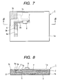
- Fig. 7 is a plan view of a voltage controlled oscillator according to a second example of the present invention
- Fig. 8 is a cross-sectional view taken along the line 8-8 of Fig. 7
- Fig. 9 is an exploded perspective view of the voltage controlled oscillator according to the second example of the present invention
- Fig. 10 is a diagram illustrating a relationship between a strip line and a conductor-deleted portion of a ground pattern in the voltage controlled oscillator according to the second example of the present invention
- Fig. 11 is a plan view showing a cut groove for frequency adjustment in the voltage controlled oscillator according to the second example of the present invention
- Fig. 12 is a schematic cross-sectional view of the cut groove for frequency adjustment in the voltage controlled oscillator according to the second example of the present invention.
- a circuit board 1 has a laminate of a plurality of thin insulating plates 2 such as resin and ceramic.
- a wiring pattern 3 made of a conductive pattern which is provided on a surface 1a of the circuit board 1 has a direct current (DC) wiring pattern 3a, a signal wiring pattern 3b, and a ground wiring pattern 3c which is disposed in an outer circumference of the circuit board 1.
- a ground conductor 4 made of a conductive pattern is provided on an entire back surface 1b of the circuit board 1.
- a U-shaped resonance strip line 5 which is made of a conductive pattern and which is provided on an inner layer of the circuit board 1 has a pair of conductors 5a arranged to face each other and spaced at a predetermined gap from each other, connection portions 5b and 5c respectively provided at one ends of the pair of conductors 5a, and a connecting conductor 5d for connecting the other ends of the pair of conductors 5a to each other.
- connection portion 5b of the strip line 5 is connected to a ground conductor 4 via a connection conductor (through hole), which is not shown.
- connection portion 5c is connected to the signal wiring pattern 3b via a connection conductor (through hole) 6.
- an entire back surface of the strip line 5 faces the ground conductor 4 and inner sides 5e disposed at an inside of the strip line in an U shape have a high current density.
- a ground pattern 7 made of a conductive pattern is provided on an inner layer of the circuit board 1 located between the wiring pattern 3 and the strip line 5.
- a U-shaped conductor-deleted portion 7a is provided at a position facing a portion of a surface of the strip line 5.
- the ground pattern 7 is arranged to face the strip line 5 in a state in which the conductor-deleted portion 7a faces the vicinity including the portion having a high current density in the strip line 5.
- the conductor-deleted portion 7a faces the vicinity including the portion having a high current density in the strip line 5. Further, a portion of the ground pattern 7 faces the portion having a low current density in the strip line 5 and the conductor-deleted portion 7a faces the strip line 5 in a range of from 50 percent to 80 percent of the surface area of the strip line 5.
- a relationship between the conductor-deleted portion 7a of the ground pattern 7 and the strip line 5 is the same as described above.
- a relationship between the conductor-deleted portion 7a of the ground pattern 7 and the wiring pattern 3 is such that the direct current (DC) wiring pattern 3a and the ground wiring pattern 3c face the conductor-deleted portion 7a.
- the direct current (DC) wiring pattern 3a and the ground wiring pattern 3c face the conductor-deleted portion 7a.
- any one of the direct current wiring pattern 3a and the ground wiring pattern 3c may face the conductor-deleted portion 7a.
- various electronic parts 8 including a capacitor 8a is mounted, such that a desired electrical circuit (oscillation circuit) is formed.
- the capacitor 8a is connected to the connection portion 5c of the strip line 5 via the signal wiring pattern 3b and the connection conductor 6.
- the voltage controlled oscillator of the present invention is formed.
- a method for adjusting a frequency will be described with reference to Figs. 5 and 6.
- a cutting method such as a laser from the back surface 1b of the circuit board 1.
- a cut groove 5f is provided in the strip line 5.
- the cut groove 5f is formed by deleting the portion of the inner sides 5e having high current densities, which are disposed at the inside of the U-shaped strip line 5, within a range of the conductor-deleted portion 7a of the ground pattern 7.
- the strip line 5 having the U shape is described, but the strip line 5 may be formed in a linear shape or a zigzag shape.
- Figs. 7 to 12 show a voltage controlled oscillator according to a second example of the present invention.
- a strip line 5 has a pair of conductors 5a arranged to face each other and spaced at a predetermined gap from each other, connection portions 5b and 5c provided at one ends of the pair of conductors 5a, and a connecting conductor 5d for connecting the other ends of the pair of conductors 5a to each other.
- a band-shaped protruding conductor 5h which protrudes from an outer side 5g of the connecting conductor 5d opposite to the connection portions 5b and 5c.
- the strip line 5 has a substantially Y shape.
- a conductor-deleted portion 7a of a ground pattern 7 has a U-shaped portion facing the vicinity including a portion having a high current density in the strip line 5 and a band-shaped portion facing a central portion of the protruding conductor 5h.
- the conductor-deleted portion 7a has a substantially Y shape.
- a cut groove 5f is provided by cutting a portion of the connecting conductor 5d having a high current density in a widthwise direction of the connecting conductor, to thereby reach the protruding conductor 5h.
- the conductor-deleted portion 7a also faces the strip line 5 in a range of from 50 percent to 80 percent of the surface area of the strip line 5.
- a voltage controlled oscillator comprises a circuit board having a laminate of a plurality of insulating plates, a wiring pattern formed on a surface of the circuit board, an electronic part mounted on the surface of the circuit board, a resonance strip line provided on an inner layer of the circuit board, and a ground pattern formed on an inner layer of the circuit board which is disposed between the wiring pattern and the strip line. Further, a conductor-deleted portion is provided in the ground pattern, and the ground pattern faces the strip line in a state in which the conductor-deleted portion faces the vicinity including a portion having a high current density in the strip line.
- the strip line has a pair of conductors arranged to face each other and spaced at a predetermined gap from each other, connection portions respectively provided at one ends of the pair of conductors, and a connecting conductor for connecting the other ends of the pair of conductors to each other.
- the strip line has a U shape.
- the strip line can be miniaturized and the portion having a high current density can be concentrated at inner sides having a U shape. Therefore, the portion having a high current density in the strip line can be integrated small and also the conductor-deleted portion can be small. As a result, it is possible to realize a favorable shield characteristic.
- a cut groove for frequency adjustment is formed in a portion having a high current density in the strip line.
- the cut groove is formed in a range of the conductor-deleted portion, the cut groove having a high current density is opened through the conductor-deleted portion. Therefore, the reductions of inductance and Q can be small.
- a band-shaped protruding conductor which protrudes from a side of the connecting conductor opposite to the connection portions is provided in the connecting conductor of the strip line.
- the cut groove is formed in a range of the conductor-deleted portion, the cut groove having a high current density is opened through the conductor-deleted portion. Therefore, the reductions of inductance and Q can be small.
- the conductor-deleted portion faces the strip line in a range of from 50 percent to 80 percent of the surface area of the strip line.
- the reductions of inductance and Q can be small by means of the conductor-deleted portion having a large area.
- the portion of the strip line having a relatively small area is shield by means of the ground pattern which is disposed between the wiring line and the strip line. Therefore, it is possible to realize a favorable shield characteristic.
- the wiring pattern which is arranged at a position facing the conductor-deleted portion is formed with a ground wiring pattern or/and a direct current (DC) wiring pattern.
- DC direct current
Landscapes
- Engineering & Computer Science (AREA)
- Microelectronics & Electronic Packaging (AREA)
- Inductance-Capacitance Distribution Constants And Capacitance-Resistance Oscillators (AREA)
Abstract
There is provided a voltage controlled oscillator
having a favorable shield characteristic between a strip
line and a wiring pattern and being small in reduction of
inductance and Q. The voltage controlled oscillator
comprises a circuit board having a laminate of a
plurality of insulating plates (2), a wiring pattern (3)
formed on a surface of the circuit board (1), an electronic
part (8) mounted on the surface of the circuit board (1), a
resonance strip line (5) provided on an inner layer of the
circuit board (1), and a ground pattern (7) formed on an
inner layer of the circuit board (1) which is disposed
between the wiring pattern (3) and the strip line (5).
Further, an opening (7a) in the ground
pattern (7) faces the vicinity including a portion having a
high current density in the strip line (5). Thus,
reductions of inductance and Q are small. In addition, a
portion of the strip line (5) is shielded by means of the
ground pattern (7) with respect to the wiring pattern (3).
As a result, a voltage controlled oscillator having a
favorable shield characteristic can be obtained.
Description
- The present invention relates to a voltage controlled oscillator that is suitably used for a cellular phone or the like.
- A conventional voltage controlled oscillator will be described with reference to the drawings. Fig. 13 is an exploded perspective view of the conventional voltage controlled oscillator, and Fig. 14 is a cross-sectional view of essential parts of the conventional voltage controlled oscillator.
- Next, a configuration of the conventional voltage controlled oscillator will be described with reference to Figs. 13 and 14. A
circuit board 51 comprises a laminate of a plurality of thininsulating plates 52. On asurface 51a of thecircuit board 51, awiring pattern 53 made of a conductive pattern is provided. In addition, on anentire back surface 51b of thecircuit board 51, aground conductor 54 made of a conductive pattern is provided. - Further, on an inner layer of the
circuit board 51, an L-shapedresonance strip line 55 made of a conductive pattern is provided. Theresonance strip line 55 hasconnection portions - Furthermore, an entire back surface of the
strip line 55 faces theground conductor 54. In addition, theconnection portion 55a of thestrip line 55 is connected to theground conductor 54 and theconnection portion 55b thereof is connected to thewiring pattern 53. - Furthermore, on an inner layer of the
circuit board 51 which is disposed between thewiring pattern 53 and thestrip line 55, a ground pattern.56 made of a conductive pattern is provided. In addition, theground pattern 56 has a conductor-deletedportion 56a which is provided at a position facing the surface of thestrip line 55. - Further, the conductor-deleted
portion 56a of theground pattern 56 faces the entire surface of thestrip line 55 and theground pattern 56 is connected to theground conductor 54 on the back surface of thecircuit board 51. - Furthermore, on the
surface 51a of thecircuit board 51, variouselectronic parts 57 including acapacitor 57a and so on are mounted, such that a desired electrical circuit (oscillation circuit) is formed. When theelectronic parts 57 are mounted on thecircuit board 51, thecapacitor 57a is connected to theconnection portion 55b of the strip line 55 (for example, see Japanese Unexamined Patent Application Publication No. 5-136612). - Such a conventional voltage controlled oscillator has a configuration that the
ground pattern 56 does not exist on the surface of thestrip line 55 and the entire back surface of thestrip line 55 faces theground conductor 54, and thus reductions of inductance and Q are small. However, since the entire surface of thestrip line 55 faces thesurface 51a of thecircuit board 51 through the conductor-deletedportion 56a, a shield characteristic between thestrip line 55 and thewiring pattern 53 is deteriorated. - As described above, according to the conventional voltage controlled oscillator, since the entire surface of the
strip line 55 faces thesurface 51a of thecircuit board 51 through the conductor-deletedportion 56a which is provided in theground pattern 56, the shield characteristic between thestrip line 55 and thewiring pattern 53 is deteriorated. - Accordingly, it is an object of the present invention to provide a voltage controlled oscillator having an excellent shield characteristic between a strip line and a wiring pattern and being small in reduction of inductance and Q.
- In order to solve the above problems, according to a first aspect of the present invention, there is provided a voltage controlled oscillator comprising a circuit board having a laminate of a plurality of insulating plates, a wiring pattern formed on a surface of the circuit board, an electronic part mounted on the surface of the circuit board, a resonance strip line provided on an inner layer of the circuit board, and a ground pattern formed on an inner layer of the circuit board which is disposed between the wiring pattern and the strip line. Further, a conductor-deleted portion is provided in the ground pattern, and the ground pattern faces the strip line in a state in which the conductor-deleted portion faces the vicinity including a portion having a high current density in the strip line.
- Further, according to a second aspect of the present invention, the strip line has a pair of conductors arranged to face each other and spaced at a predetermined gap from each other, connection portions respectively provided at one ends of the pair of conductors, and a connecting conductor for connecting the other ends of the pair of conductors to each other. Here, the strip line has a U shape.
- Further, according to a third aspect of the present invention, a cut groove for frequency adjustment is provided in the portion having a high current density of the strip line.
- Further, according to a fourth aspect of the present invention, the cut groove is formed in a range of the conductor-deleted portion.
- Further, according to a fifth aspect of the present invention, a band-shaped protruding conductor which protrudes from a side of the connecting conductor opposite to the connection portions is provided in the connecting conductor of the strip line.
- Furthermore, according to a sixth aspect of the present invention, by cutting a portion of the connecting conductor having a high current density in a widthwise direction of the connecting conductor, a cut groove for frequency adjustment is provided in the strip line to reach the connecting conductor.
- Furthermore, according to a seventh aspect of the present invention, the cut groove is formed in a range of the conductor-deleted portion.
- In addition, according to an eighth aspect of the present invention, the conductor-deleted portion faces the strip line in a range of from 50 percent to 80 percent of the surface area of the strip line.
- In addition, according to a ninth aspect of the present invention, the wiring pattern which is arranged at a position facing the conductor-deleted portion is formed with a ground wiring pattern or/and a direct current (DC) wiring pattern.
-
- Fig. 1 is a plan view of a voltage controlled oscillator according to a first example of the present invention;
- Fig. 2 is a cross-sectional view taken along the line 2-2 of Fig. 1;
- Fig. 3 is an exploded perspective view of the voltage controlled oscillator according to the first example of the present invention;
- Fig. 4 is a diagram illustrating a relationship between a strip line and a conductor-deleted portion of a ground pattern in the voltage controlled oscillator according to the first example of the present invention;
- Fig. 5 is a plan view showing a cut groove for frequency adjustment in the voltage controlled oscillator according to the first example of the present invention;
- Fig. 6 is a schematic cross-sectional view of the cut groove for frequency adjustment in the voltage controlled oscillator according to the first example of the present invention;
- Fig. 7 is a plan view of a voltage controlled oscillator according to a second example of the present invention;
- Fig. 8 is a cross-sectional view taken along the line 8-8 of Fig. 7;
- Fig. 9 is an exploded perspective view of the voltage controlled oscillator according to the second example of the present invention;
- Fig. 10 is a diagram illustrating a relationship between a strip line and a conductor-deleted portion of a ground pattern in the voltage controlled oscillator according to the second example of the present invention;
- Fig. 11 is a plan view showing a cut groove for frequency adjustment in the voltage controlled oscillator according to the second example of the present invention;
- Fig. 12 is a schematic cross-sectional view of the cut groove for frequency adjustment in the voltage controlled oscillator according to the second example of the present invention;
- Fig. 13 is an exploded perspective view of a conventional voltage controlled oscillator; and
- Fig. 14 is a cross-sectional view of essential parts of the conventional voltage controlled oscillator.
-
- A voltage controlled oscillator of the present invention will be described with reference to the drawings. Fig. 1 is a plan view of a voltage controlled oscillator according to a first example of the present invention, Fig. 2 is a cross-sectional view taken along the line 2-2 of Fig. 1, and Fig. 3 is an exploded perspective view of the voltage controlled oscillator according to the first example of the present invention. Further, Fig. 4 is a diagram illustrating a relationship between a strip line and a conductor-deleted portion of a ground pattern in the voltage controlled oscillator according to the first example of the present invention, Fig. 5 is a plan view showing a cut groove for frequency adjustment in the voltage controlled oscillator according to the first example of the present invention, and Fig. 6 is a schematic cross-sectional view of the cut groove for frequency adjustment in the voltage controlled oscillator according to the first example of the present invention.
- Further, Fig. 7 is a plan view of a voltage controlled oscillator according to a second example of the present invention, Fig. 8 is a cross-sectional view taken along the line 8-8 of Fig. 7, and Fig. 9 is an exploded perspective view of the voltage controlled oscillator according to the second example of the present invention. In addition, Fig. 10 is a diagram illustrating a relationship between a strip line and a conductor-deleted portion of a ground pattern in the voltage controlled oscillator according to the second example of the present invention, Fig. 11 is a plan view showing a cut groove for frequency adjustment in the voltage controlled oscillator according to the second example of the present invention, and Fig. 12 is a schematic cross-sectional view of the cut groove for frequency adjustment in the voltage controlled oscillator according to the second example of the present invention.
- Next, a configuration of a voltage controlled oscillator according to a first example of the present invention will be described with reference to Figs 1 to 6. A
circuit board 1 has a laminate of a plurality of thininsulating plates 2 such as resin and ceramic. - A
wiring pattern 3 made of a conductive pattern which is provided on asurface 1a of thecircuit board 1 has a direct current (DC)wiring pattern 3a, asignal wiring pattern 3b, and aground wiring pattern 3c which is disposed in an outer circumference of thecircuit board 1. On anentire back surface 1b of thecircuit board 1, aground conductor 4 made of a conductive pattern is provided. - Further, a U-shaped
resonance strip line 5 which is made of a conductive pattern and which is provided on an inner layer of thecircuit board 1 has a pair ofconductors 5a arranged to face each other and spaced at a predetermined gap from each other,connection portions conductors 5a, and a connectingconductor 5d for connecting the other ends of the pair ofconductors 5a to each other. - And then, the
connection portion 5b of thestrip line 5 is connected to aground conductor 4 via a connection conductor (through hole), which is not shown. At the same time, as shown in Fig. 2, theconnection portion 5c is connected to thesignal wiring pattern 3b via a connection conductor (through hole) 6. - In the
strip line 5 having the above-mentioned structure, an entire back surface of thestrip line 5 faces theground conductor 4 andinner sides 5e disposed at an inside of the strip line in an U shape have a high current density. - In addition, on an inner layer of the
circuit board 1 located between thewiring pattern 3 and thestrip line 5, aground pattern 7 made of a conductive pattern is provided. In theground pattern 7, a U-shaped conductor-deletedportion 7a is provided at a position facing a portion of a surface of thestrip line 5. - As shown in Fig. 4, the
ground pattern 7 is arranged to face thestrip line 5 in a state in which the conductor-deletedportion 7a faces the vicinity including the portion having a high current density in thestrip line 5. - Specifically, the conductor-deleted
portion 7a faces the vicinity including the portion having a high current density in thestrip line 5. Further, a portion of theground pattern 7 faces the portion having a low current density in thestrip line 5 and the conductor-deletedportion 7a faces thestrip line 5 in a range of from 50 percent to 80 percent of the surface area of thestrip line 5. - In addition, a relationship between the conductor-deleted
portion 7a of theground pattern 7 and thestrip line 5 is the same as described above. However, as shown in Fig. 1, a relationship between the conductor-deletedportion 7a of theground pattern 7 and thewiring pattern 3 is such that the direct current (DC)wiring pattern 3a and theground wiring pattern 3c face the conductor-deletedportion 7a. - In the present example, the direct current (DC)
wiring pattern 3a and theground wiring pattern 3c face the conductor-deletedportion 7a. Alternatively, however, any one of the directcurrent wiring pattern 3a and theground wiring pattern 3c may face the conductor-deletedportion 7a. - Furthermore, on the
surface 1a of thecircuit board 1, variouselectronic parts 8 including acapacitor 8a is mounted, such that a desired electrical circuit (oscillation circuit) is formed. When theelectronic parts 8 are mounted on thecircuit board 1, thecapacitor 8a is connected to theconnection portion 5c of thestrip line 5 via thesignal wiring pattern 3b and theconnection conductor 6. - In such a manner, the voltage controlled oscillator of the present invention is formed. Next, a method for adjusting a frequency will be described with reference to Figs. 5 and 6. First, a portion of the
ground conductor 4, the insulatingplate 2, and thestrip line 5 are deleted using a cutting method (not shown) such as a laser from theback surface 1b of thecircuit board 1. And then, as shown in Fig. 5, acut groove 5f is provided in thestrip line 5. By means of such a configuration, a frequency adjustment is performed. - In addition, the
cut groove 5f is formed by deleting the portion of theinner sides 5e having high current densities, which are disposed at the inside of theU-shaped strip line 5, within a range of the conductor-deletedportion 7a of theground pattern 7. - In addition, in the above-mentioned example, the
strip line 5 having the U shape is described, but thestrip line 5 may be formed in a linear shape or a zigzag shape. - Further, Figs. 7 to 12 show a voltage controlled oscillator according to a second example of the present invention. According to the second example, a
strip line 5 has a pair ofconductors 5a arranged to face each other and spaced at a predetermined gap from each other,connection portions conductors 5a, and a connectingconductor 5d for connecting the other ends of the pair ofconductors 5a to each other. Further, in the connectingconductor 5d, a band-shapedprotruding conductor 5h which protrudes from anouter side 5g of the connectingconductor 5d opposite to theconnection portions strip line 5 has a substantially Y shape. - In addition, a conductor-deleted
portion 7a of aground pattern 7 has a U-shaped portion facing the vicinity including a portion having a high current density in thestrip line 5 and a band-shaped portion facing a central portion of the protrudingconductor 5h. As a result, the conductor-deletedportion 7a has a substantially Y shape. Acut groove 5f is provided by cutting a portion of the connectingconductor 5d having a high current density in a widthwise direction of the connecting conductor, to thereby reach the protrudingconductor 5h. - Since other elements of the second example are the same as those of the first example, the same elements are represented by the same reference numerals, and then the description of the same elements will be omitted.
- In the second example, the conductor-deleted
portion 7a also faces thestrip line 5 in a range of from 50 percent to 80 percent of the surface area of thestrip line 5. - According to the present invention, a voltage controlled oscillator comprises a circuit board having a laminate of a plurality of insulating plates, a wiring pattern formed on a surface of the circuit board, an electronic part mounted on the surface of the circuit board, a resonance strip line provided on an inner layer of the circuit board, and a ground pattern formed on an inner layer of the circuit board which is disposed between the wiring pattern and the strip line. Further, a conductor-deleted portion is provided in the ground pattern, and the ground pattern faces the strip line in a state in which the conductor-deleted portion faces the vicinity including a portion having a high current density in the strip line.
- In such a manner, since the conductor-deleted portion of the ground pattern faces the vicinity including a portion having a high current density in the strip line, reductions of inductance and Q are small. In addition, a portion of the strip line which does not face the conductor-deleted portion faces the ground pattern, and thus a portion of the strip line is shielded by the ground pattern with respect to the wiring pattern. As a result, it is possible to obtain an excellent shield characteristic.
- In addition, the strip line has a pair of conductors arranged to face each other and spaced at a predetermined gap from each other, connection portions respectively provided at one ends of the pair of conductors, and a connecting conductor for connecting the other ends of the pair of conductors to each other. Further, the strip line has a U shape. Thus, the strip line can be miniaturized and the portion having a high current density can be concentrated at inner sides having a U shape. Therefore, the portion having a high current density in the strip line can be integrated small and also the conductor-deleted portion can be small. As a result, it is possible to realize a favorable shield characteristic.
- In addition, a cut groove for frequency adjustment is formed in a portion having a high current density in the strip line. Thus, a range of a frequency adjustment increases. As a result, it is possible to realize a favorable a frequency adjustment.
- In addition, since the cut groove is formed in a range of the conductor-deleted portion, the cut groove having a high current density is opened through the conductor-deleted portion. Therefore, the reductions of inductance and Q can be small.
- In addition, a band-shaped protruding conductor which protrudes from a side of the connecting conductor opposite to the connection portions is provided in the connecting conductor of the strip line. Thus, the cut groove for frequency adjustment can extend to the protruding conductor. Therefore, it is possible to increase a range of the frequency adjustment.
- In addition, by cutting a portion of the connecting conductor having a high current density in the strip line in a widthwise direction of the connecting conductor, a cut groove for frequency adjustment is provided to reach the protruding conductor. Therefore, it is possible to increase a range of frequency adjustment.
- In addition, since the cut groove is formed in a range of the conductor-deleted portion, the cut groove having a high current density is opened through the conductor-deleted portion. Therefore, the reductions of inductance and Q can be small.
- In addition, the conductor-deleted portion faces the strip line in a range of from 50 percent to 80 percent of the surface area of the strip line. Thus, the reductions of inductance and Q can be small by means of the conductor-deleted portion having a large area. In addition, the portion of the strip line having a relatively small area is shield by means of the ground pattern which is disposed between the wiring line and the strip line. Therefore, it is possible to realize a favorable shield characteristic.
- In addition, the wiring pattern which is arranged at a position facing the conductor-deleted portion is formed with a ground wiring pattern or/and a direct current (DC) wiring pattern. Thus, there is no need for connecting the strip line to other signal lines. Therefore, it is possible to realize a favorable electrical performance.
Claims (9)
- A voltage controlled oscillator comprising:wherein a conductor-deleted portion is provided in the ground pattern, anda circuit board having a laminate of a plurality of insulating plates;a wiring pattern formed on a surface of the circuit board;an electronic part mounted on the surface of the circuit board;a resonance strip line provided on an inner layer of the circuit board; anda ground pattern formed on an inner layer of the circuit board which is disposed between the wiring pattern and the strip line,
the ground pattern faces the strip line in a state in which the conductor-deleted portion faces the vicinity including a portion having a high current density in the strip line. - The voltage controlled oscillator according to claim 1,
wherein the strip line includes a pair of conductors arranged to face each other and spaced at a predetermined gap from each other, connection portions respectively provided at one ends of the pair of conductors, and a connecting conductor for connecting the other ends of the pair of conductors to each other, and
the strip line has a U shape. - The voltage controlled oscillator according to claim 1 or 2,
wherein a cut groove for frequency adjustment is formed in the portion having a high current density in the strip line. - The voltage controlled oscillator according to claim 3,
wherein the cut groove is formed in a range of the conductor-deleted portion. - The voltage controlled oscillator according to any of claims 2 to 4,
wherein a band-shaped protruding conductor which protrudes from a side of the connecting conductor opposite to the connection portions is provided in the connecting conductor of the strip line. - The voltage controlled oscillator according to claim 5,
wherein by cutting a portion of the connecting conductor having a high current density in the strip line in a widthwise direction of the connecting conductor, a cut groove for frequency adjustment is provided to reach a protruding conductor. - The voltage controlled oscillator according to claim 6,
wherein the cut groove is formed in a range of the conductor-deleted portion. - The voltage controlled oscillator according to any of claims 1 to 7,
wherein the conductor-deleted portion faces the strip line in a range of from 50 percent to 80 percent of the surface area of the strip line. - The voltage controlled oscillator according to any of claims 1 to 8,
wherein the wiring pattern which is arranged at a position facing the conductor-deleted portion is formed with a ground wiring pattern or/and a direct current (DC) wiring pattern.
Applications Claiming Priority (2)
| Application Number | Priority Date | Filing Date | Title |
|---|---|---|---|
| JP2003394878A JP4451119B2 (en) | 2003-11-26 | 2003-11-26 | Voltage controlled oscillator |
| JP2003394878 | 2003-11-26 |
Publications (1)
| Publication Number | Publication Date |
|---|---|
| EP1536553A1 true EP1536553A1 (en) | 2005-06-01 |
Family
ID=34463788
Family Applications (1)
| Application Number | Title | Priority Date | Filing Date |
|---|---|---|---|
| EP04027441A Withdrawn EP1536553A1 (en) | 2003-11-26 | 2004-11-18 | Voltage controlled oscillator |
Country Status (4)
| Country | Link |
|---|---|
| US (1) | US7142068B2 (en) |
| EP (1) | EP1536553A1 (en) |
| JP (1) | JP4451119B2 (en) |
| CN (1) | CN100472938C (en) |
Cited By (1)
| Publication number | Priority date | Publication date | Assignee | Title |
|---|---|---|---|---|
| US7952444B2 (en) | 2006-08-08 | 2011-05-31 | Agency For Science, Technology And Research | CMOS power oscillator with frequency modulation |
Families Citing this family (1)
| Publication number | Priority date | Publication date | Assignee | Title |
|---|---|---|---|---|
| CN108231735B (en) * | 2017-12-21 | 2020-01-14 | 南京中感微电子有限公司 | Voltage controlled oscillator |
Citations (5)
| Publication number | Priority date | Publication date | Assignee | Title |
|---|---|---|---|---|
| JPH05136612A (en) * | 1991-11-11 | 1993-06-01 | Tdk Corp | Oscillator module |
| US5227739A (en) * | 1990-12-20 | 1993-07-13 | Murata Manufacturing Co., Ltd. | Voltage controlled oscillator having a resonator |
| JP2001136028A (en) * | 1999-11-08 | 2001-05-18 | Matsushita Electric Ind Co Ltd | High frequency oscillator mounting board |
| EP1172882A2 (en) * | 2000-07-11 | 2002-01-16 | Murata Manufacturing Co., Ltd. | Resonator |
| US6388535B1 (en) * | 1999-04-19 | 2002-05-14 | Sharp Kabushiki Kaisha | Oscillator, and an oscillator characteristic adjustment method |
Family Cites Families (1)
| Publication number | Priority date | Publication date | Assignee | Title |
|---|---|---|---|---|
| JP2001060827A (en) | 1999-08-19 | 2001-03-06 | Alps Electric Co Ltd | Microstrip line type voltage controlled oscillator |
-
2003
- 2003-11-26 JP JP2003394878A patent/JP4451119B2/en not_active Expired - Fee Related
-
2004
- 2004-11-16 US US10/990,025 patent/US7142068B2/en not_active Expired - Lifetime
- 2004-11-18 EP EP04027441A patent/EP1536553A1/en not_active Withdrawn
- 2004-11-23 CN CNB2004100950937A patent/CN100472938C/en not_active Expired - Fee Related
Patent Citations (5)
| Publication number | Priority date | Publication date | Assignee | Title |
|---|---|---|---|---|
| US5227739A (en) * | 1990-12-20 | 1993-07-13 | Murata Manufacturing Co., Ltd. | Voltage controlled oscillator having a resonator |
| JPH05136612A (en) * | 1991-11-11 | 1993-06-01 | Tdk Corp | Oscillator module |
| US6388535B1 (en) * | 1999-04-19 | 2002-05-14 | Sharp Kabushiki Kaisha | Oscillator, and an oscillator characteristic adjustment method |
| JP2001136028A (en) * | 1999-11-08 | 2001-05-18 | Matsushita Electric Ind Co Ltd | High frequency oscillator mounting board |
| EP1172882A2 (en) * | 2000-07-11 | 2002-01-16 | Murata Manufacturing Co., Ltd. | Resonator |
Non-Patent Citations (2)
| Title |
|---|
| PATENT ABSTRACTS OF JAPAN vol. 017, no. 518 (E - 1434) 17 September 1993 (1993-09-17) * |
| PATENT ABSTRACTS OF JAPAN vol. 2000, no. 22 9 March 2001 (2001-03-09) * |
Cited By (1)
| Publication number | Priority date | Publication date | Assignee | Title |
|---|---|---|---|---|
| US7952444B2 (en) | 2006-08-08 | 2011-05-31 | Agency For Science, Technology And Research | CMOS power oscillator with frequency modulation |
Also Published As
| Publication number | Publication date |
|---|---|
| US20050110585A1 (en) | 2005-05-26 |
| CN100472938C (en) | 2009-03-25 |
| JP2005159692A (en) | 2005-06-16 |
| CN1622448A (en) | 2005-06-01 |
| JP4451119B2 (en) | 2010-04-14 |
| US7142068B2 (en) | 2006-11-28 |
Similar Documents
| Publication | Publication Date | Title |
|---|---|---|
| KR100266376B1 (en) | Surface Mount Antennas & Communications Equipment | |
| KR100414635B1 (en) | Antenna system and radio unit using the same | |
| EP1227540A1 (en) | Partial ground connection of a metal housing for realising certain electrical lenghts for the ground connection of a chip antenna | |
| JPH0653733A (en) | Resonator antenna | |
| JPH06260949A (en) | Wireless device | |
| JP2002313676A (en) | Surface mount type capacitors | |
| US6310525B1 (en) | Dielectric laminated device and its manufacturing method | |
| EP0707355B1 (en) | Antenna device | |
| JP3374604B2 (en) | Wireless communication device | |
| US7142068B2 (en) | Voltage controlled oscillator small in reduction of inductance and Q | |
| JP2004064353A (en) | Antenna component, antenna system, and communication apparatus | |
| JPH05206730A (en) | Voltage controlled oscillator and adjustment method of its oscillating frequency | |
| JP2001028504A (en) | Circulator | |
| US6002366A (en) | Surface mount antenna and communication apparatus using same | |
| JPH11214927A (en) | High frequency module | |
| EP1172882B1 (en) | Resonator | |
| HK1002133A1 (en) | High gain portable radio selective call receiver using a microstrip construction for inter-board connections | |
| HK1002133B (en) | High gain portable radio selective call receiver using a microstrip construction for inter-board connections | |
| JPH09167902A (en) | Dielectric filter | |
| JP2732150B2 (en) | Dielectric band stop filter | |
| JPH1098315A (en) | Dielectric laminated device, manufacturing method thereof and mobile communication device | |
| JP3250378B2 (en) | Dielectric filter | |
| JPH04188902A (en) | Dielectric resonator and band blocking filter using the same | |
| JP3441975B2 (en) | High frequency package | |
| JP2002368518A (en) | Surface mounting type antenna and communication equipment mounted with the same |
Legal Events
| Date | Code | Title | Description |
|---|---|---|---|
| PUAI | Public reference made under article 153(3) epc to a published international application that has entered the european phase |
Free format text: ORIGINAL CODE: 0009012 |
|
| AK | Designated contracting states |
Kind code of ref document: A1 Designated state(s): AT BE BG CH CY CZ DE DK EE ES FI FR GB GR HU IE IS IT LI LU MC NL PL PT RO SE SI SK TR |
|
| AX | Request for extension of the european patent |
Extension state: AL HR LT LV MK YU |
|
| AKX | Designation fees paid | ||
| STAA | Information on the status of an ep patent application or granted ep patent |
Free format text: STATUS: THE APPLICATION IS DEEMED TO BE WITHDRAWN |
|
| 18D | Application deemed to be withdrawn |
Effective date: 20051202 |
|
| REG | Reference to a national code |
Ref country code: DE Ref legal event code: 8566 |