BACKGROUND OF THE INVENTION
-
The present invention relates to an electroluminescent element and a
lighting unit including the electroluminescent element.
-
An electroluminescent element or an EL element is formed by layering an
electroluminescent material and the like on its substrate. The EL element, which
emits light from the side of a glass substrate, generally has a transparent
electrode on the side of the substrate relative to its luminescent layer (EL layer)
containing an electroluminescent material and also has a metallic electrode on
the opposite side to the substrate. In order to prevent the EL layer from degrading
due to moisture or oxygen, the transparent electrode, the organic layer and the
metallic electrode are sealed by a sealing member.
-
On the other hand, there is an invention which does not provide a sealing
member on a metallic electrode for enhancing heat radiation performance, as
disclosed in Examined Japanese Patent Publication No. 6-32297. There is
another invention that utilizes a thickened metallic electrode as a sealing member,
as disclosed in Unexamined Japanese Patent Publication No. 2003-217854.
-
A portion of an electrode which is not sealed by the sealing member may
be used for a terminal which is electrically connected to a power source. Also, a
plurality of EL elements may be arranged to form a lighting unit.
SUMMARY OF THE INVENTION
-
In accordance with the present invention, an electroluminescent element
has a substrate, a first electrode, a luminescent layer, a second electrode, a first
terminal and a second terminal. The first electrode has a first surface and a
second surface that is opposite to the first surface. The first electrode is layered
on the substrate so as to contact the substrate on its first surface. The
luminescent layer, which contains a light-emitting layer, is layered on the first
electrode so as to contact the second surface of the first electrode. The second
electrode has a first surface and a second surface that is opposite to the first
surface. The second electrode is layered on the luminescent layer so as to
contact the luminescent layer on its first surface. The second surface of the
second electrode is at least partially exposed. The first terminal is provided on the
second surface of the first electrode at a portion that does not contact the
luminescent layer. The second terminal is partially formed in the exposed portion
of the second surface of the second electrode. At least one of the first electrode
and the second electrode is transparent. The first terminal and the second
terminal are connected to a power source.
-
Other aspects and advantages of the invention will become apparent from
the following description, taken in conjunction with the accompanying drawings,
illustrating by way of example the principles of the invention.
BRIEF DESCRIPTION OF THE DRAWINGS
-
The features of the present invention that are believed to be novel are set
forth with particularity in the appended claims. The invention together with objects
and advantages thereof, may best be understood by reference to the following
description of the presently preferred embodiments together with the
accompanying drawings in which:
- FIG. 1A is a schematic cross-sectional view of an organic
electroluminescent element according to a first preferred embodiment of the
present invention;
- FIG. 1B is a schematic front end view of the organic electroluminescent
element according to the first preferred embodiment of the present invention;
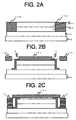
- FIG. 2A is a schematic view showing one aspect of a manufacturing
process of the organic electroluminescent element according to the first preferred
embodiment of the present invention;
- FIG. 2B is a schematic view showing another aspect of the manufacturing
process of the organic electroluminescent element according to the first preferred
embodiment of the present invention;
- FIG. 2C is a schematic view showing yet another aspect of the
manufacturing process of the organic electroluminescent element according to
the first preferred embodiment of the present invention;
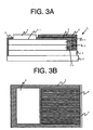
- FIG. 3A is a schematic cross-sectional view of an organic
electroluminescent element according to a second preferred embodiment of the
present invention;
- FIG. 3B is a schematic front end view of the organic electroluminescent
element according to the second preferred embodiment of the present invention;
- FIG. 4A is a schematic back side view of a lighting unit according to a third
preferred embodiment of the present invention; and
- FIG. 4B is a schematic cross-sectional view of the lighting unit according
to the third preferred embodiment of the present invention.
-
DETAILED DESCRIPTION OF THE PREFERRED EMBODIMENTS
-
A first preferred embodiment of an electroluminescent element, which is
applied to an organic electroluminescent element or an organic EL element 1
employing an organic compound in its electroluminescent layer (EL layer)
according to the present invention, will now be described with reference to FIGS.
1A through 2C. It is noted that a slanted line for indicating cross-section is partially
omitted, and the same components are indicated with the same slanted lines for
easier recognition irrespective of the cross-sectional view and the front end view
in FIGS. 1A through 2C.
-
As shown in FIG. 1A, the organic EL element 1 has an anode or a first
electrode 3, an organic layer 4 containing a light-emitting layer, and a cathode or
a second electrode 5 on its substrate 2 in this order. In other words, the anode 3
has a first surface and a second surface that is opposite to the first surface, and is
layered on the substrate 2 so as to contact the substrate 2 on its first surface. The
organic layer 4 is layered on the anode 3 so as to contact the second surface of
the anode 3. The cathode 5 has a first surface and a second surface that is
opposite to the first surface. The cathode 5 is layered on the organic layer 4 so as
to contact the organic layer 4 on its first surface. The anode 3 includes a contact
portion 31 that contacts the organic layer 4 and a non-contact portion 32 that does
not contact the organic layer 4. In the first preferred embodiment, the non-contact
portion 32 is provided at a periphery of the anode 3. The organic layer 4 contacts
the anode 3 by the entire surface of one side 41 and contacts the cathode 5 by
the entire surface of the other side 42.
-
A sealing layer or a sealing member 6 is deposited to cover the end
surface of the organic layer 4, the end surface of the cathode 5, and the periphery
of an opposite surface 51 to a surface that contacts the organic layer 4 of the
cathode 5. A portion, which is not covered with the sealing layer 6 in the opposite
surface 51 to the surface that contacts the organic layer 4 of the cathode 5, is
exposed thus forming a cathode terminal or a second terminal 8. Also, an anode
terminal or a first terminal 9 is provided at the non-contact portion 32, which does
not contact the organic layer 4 of the anode 3. Accordingly, in the organic EL
element 1 according to the first preferred embodiment, as seen from the side of
the cathode 5, the cathode terminal 8 is positioned at the center, and the anode
terminal 9 is arranged around the cathode terminal 8 via the sealing layer 6, as
shown in FIG. 1B.
-
Each component of the organic EL element 1 will now be described.
-
The substrate 2 is made of glass in the first preferred embodiment but
may be made of any transparent materials having a sufficient strength when the
anode 3 and the organic layer 4 are deposited thereon. Other than glass, such a
material may include a transparent resin.
-
The anode 3 supplies positive holes to the organic layer 4, and light
emitted from the organic layer 4 is emitted outside through the anode 3 and the
substrate 2 in the first preferred embodiment, so that the anode 3 needs to be
transparent. In the first preferred embodiment, a material for the anode 3 is ITO
(indium tin oxide), but the material may be IZO (indium zinc oxide) and the like.
-
The organic layer 4 needs to have at least a light-emitting layer. The
light-emitting layer emits light by recombination of positive holes supplied from the
anode 3 and electrons supplied from the cathode 5. The light-emitting layer may
be made of a single organic compound or may be made of plural organic
compounds.
-
When the light-emitting layer is made of plural organic compounds, each
layer made of an organic compound may be plurally layered, or may be made of a
layer which mixes plural organic compounds.
-
The organic layer 4 may partially or wholly include a positive hole injection
layer or a positive hole transport layer for efficiently transporting positive holes
supplied from the anode 3 to the light-emitting layer, and an electron injection
layer or an electron transport layer for efficiently transporting electrons supplied
from the cathode 5 to the light-emitting layer, in addition to the light-emitting layer.
Also, a single layer may have plural functions.
-
Specifically, the organic layer 4 may be constituted of the following layer
structures.
- (Anode) / Positive Hole Injection Layer / Positive Hole Transport Layer / Light-emitting
Layer / Electron Transport Layer / Electron Injection Layer / (Cathode)
- (Anode) / Positive Hole Injection Layer / Positive Hole Transport Layer / Light-emitting
Layer / Electron Injection Transport Layer / (Cathode)
- (Anode) / Positive Hole Injection Transport Layer / Light-emitting Layer / Electron
Transport Layer / Electron Injection Layer / (Cathode)
- (Anode) / Positive Hole Injection Transport Layer / Light-emitting Layer / Electron
Injection Transport Layer / (Cathode)
- (Anode) / Positive Hole Transport Layer / Light-emitting Layer / Electron
Transport Layer / Electron Injection Layer / (Cathode)
- (Anode) / Positive Hole Transport Layer / Light-emitting Layer / Electron
Transport Layer / (Cathode)
- (Anode) / Positive Hole Transport Layer / Electron Transport
Light-emitting Layer / (Cathode)
- (Anode) / Light-emitting Layer / (Cathode)
-
The organic layer 4 according to the first preferred embodiment is
constituted of a positive hole transport layer, a light-emitting layer, an electron
transport layer and an electron injection layer, and has a three-layer structure in
which a green light-emitting layer, a blue light-emitting and a red light-emitting
layer are layered from the contact portion 31 of the anode 3.
-
The cathode 5 supplies electrons to the organic layer 4, and is made of a
material having an electrical conductivity and preferably made of a material
having a low resistivity. Such a material includes a metal, an alloy and a metallic
mixture. In the first preferred embodiment, the cathode 5 is made of aluminum.
-
Since a non-covered portion of the cathode 5 that is not covered with the
sealing layer 6 is exposed, to prevent a substance such as moisture and oxygen
from degrading the organic layer 4 by entering into the organic EL element 1
through the portion 51, the thickness of the cathode 5 is preferably 0.5 µm or
above, and more preferably 1.5 µm or above. Also, when the cathode 5 is
formed by vapor deposition, the thickness of the cathode 5 is preferably 5 µm or
below, and more preferably 3 µm or below. When the cathode terminal 8 is
provided on the portion 51 that is not covered with the sealing layer 6 by vapor
deposition, bonding, and the like after forming the cathode 5, the thickness of the
cathode terminal 8 is preferably 1 mm or below, and more preferably 300 µm or
below.
-
The sealing layer 6 serves to prevent the organic layer 4 from being
degraded due to moisture in the atmosphere or oxygen, and is made of a material
having a high airtightness. Such a material includes organic polymeric materials,
inorganic materials, and the like. The organic polymeric materials include epoxy
resin, silicone resin, polystyrene resin and the like. The inorganic material
includes glass, metal oxide, metal nitride and the like. In the first preferred
embodiment, a silicon nitride layer, which is an inorganic material, is used as the
sealing layer 6.
-
The anode terminal 7 is connected to a power source (not shown) and
serves to supply positive holes to the anode 3. The anode terminal 7 may be
made of the same material as the cathode 5. In the first preferred embodiment,
aluminum is employed for the anode terminal 7 as well as the cathode 5.
-
A method of manufacturing the organic EL element 1 will now be
described with reference to FIGS. 2A through 2C.
-
The substrate 2, which is provided with the anode 3 of a desired shape on
its surface, is washed and after that is placed in a vacuum evaporator (not shown).
In the vacuum evaporator, as shown in FIG. 2A, a positive hole transport layer is
vapor-deposited after a mask 100 is placed on the periphery of the anode 3. Then,
the light-emitting layer is vapor-deposited on the positive hole transport layer, in
the order of a green light-emitting, a blue light-emitting and a red light-emitting.
Subsequently, an electron transport layer and an electron injection layer are
vapor-deposited on the light-emitting layer, in this order, thus forming the organic
layer 4. Additionally, aluminum is vapor-deposited on the organic layer 4 to form
the cathode 5. After forming the cathode 5, the mask 100 is removed.
-
As shown in FIG. 2B, a mask 101 is placed to form the sealing layer 6.
After forming the sealing layer 6, the mask 101 is removed. After that, as shown in
FIG. 2C, a mask 102 is placed, and aluminum is vapor-deposited, thus forming
the anode terminal 9.
-
The operation of the organic EL element 1 will now be described.
-
The positive electrode of a direct-current power source (not shown) is
connected to the anode terminal 9, and the negative electrode thereof is
connected to the cathode terminal 8 thereby applying a voltage so that the electric
potential of the anode terminal 9 is higher than that of the cathode terminal 8.
Positive holes are supplied, from the positive electrode of the direct-current power
source, through the anode terminal 9 and the anode 3 to the organic layer 4. The
positive holes, which have reached the anode 3, move to the light-emitting layer
through the positive hole transport layer in the organic layer 4. On the other hand,
electrons are supplied from the negative electrode of the direct-current power
source through the cathode terminal 9 to the cathode 5. The electrons, which
have reached the cathode 5, advance to the light-emitting layer through the
electron injection layer and the electron transport layer in the organic layer 4.
-
Positive holes from the anode 3, which have reached the light-emitting
layer, and electrons from the cathode 5, which have reached to the light-emitting
layer, recombine to generate excitons thereby emitting light when the excitons
return to a ground state. In the first preferred embodiment, the light-emitting layer
is a three-layer structure, and these three layers respectively emit green light,
blue light and red light. These lights are mixed together and are visible as white
light.
-
A portion of light emitted from the light-emitting layer is directly emitted
outside from the substrate 2 through the anode 3. The other light reaches the
cathode 5. The cathode 5, which is made of aluminum, has a light reflectivity, so
that light which has reached the cathode 5 is reflected and is emitted outside from
the substrate 2 through the organic layer 4 and the anode 5.
-
According to the first preferred embodiment, the following advantageous
effects are obtained.
- (1) The non-covered portion of the cathode 5 which is not covered with the
sealing layer 6 forms the cathode terminal 8.
Since the entire surface of the opposite surface 51 of the cathode 5 is not
covered with the sealing layer 6, and only its periphery is covered with the sealing
layer 6, the exposed portion, which is not covered with the sealing layer 6, is used
as the cathode terminal 8, and is connected to an external power source.
Accordingly, since the cathode terminal 8 may be provided on an opposite side of
a light output side of the organic EL element 1, while the cathode terminal 8 need
not be provided on a portion other than the portion of the substrate 2 where the
organic layer 4 is provided, the area of the substrate 2 for the same area of the
organic layer 4 may be reduced. In other words, the area contributing to light
emission may be increased in the area of the substrate 2. - (2) The cathode 5 has an airtightness.
Since the cathode 5 has a thickness of 0.5 µm or above, the cathode 5
has a sufficient airtightness. That is, the cathode 5 prevents a substance such as
moisture and oxygen from degrading the organic layer 4 by entering into the
organic EL element 1 through the cathode 5. Therefore, even if the entire surface
of the opposite surface 51 of the cathode 5 is not covered with the sealing layer 6,
and the exposed portion, which is not covered with the sealing layer 6, is used as
the cathode terminal 8, the organic EL element 1 is prevented from degrading due
to moisture or oxygen entering from the outside and shortening the life thereof.
- (3) The organic layer 4 is not exposed.
After the organic layer 4 is formed to contact the anode 3, the cathode 5 is
formed to contact the entire surface of the opposite surface 42 of the organic layer
4. Since the sealing layer 6 is deposited on that basis, the sealing layer 6 seals
the entire portion, other than the surface 41 and the surface 42. Accordingly, the
organic layer 4 is covered on its outer surface with the anode 3, the cathode 5 and
the sealing layer 6, so that there is no exposed portion. Therefore, degradation of
the organic layer 4 due to entry of moisture or oxygen is prevented. - (4) The organic EL element 1 emits white light.
The light-emitting layer of the organic layer 4 is constituted of a layer for
emitting green light, a layer for emitting blue light and a layer for emitting red light.
As voltage is applied to the organic EL element 1, these layers simultaneously
emit light thereby emitting white light as a whole. Since the white light emitted
from the organic EL element 1 has peaks in a red color spectral range, a blue
color spectral range and a green color spectral range, clear color is generated
when displaying an image through an RGB color filter. - (5) Utilization rate of light is high.
An aluminum thin film having a light reflectivity is employed as the
cathode 5. Therefore, light-traveling from the light-emitting layer to the cathode 5
is reflected toward the substrate 2 on the cathode 5, and the reflected light is
partially emitted outside from the substrate 2. Accordingly, in comparison to the
cathode 5 made of a material having no light reflectivity, more light that is emitted
from the light-emitting layer is emitted from the substrate 2.
A second preferred embodiment of the present invention will now be
described with reference to FIGS. 3A and 3B. The second preferred embodiment
is different from the first preferred embodiment in that the positions of the anode
terminal 9 and the cathode terminal 8 are different. The same reference numerals
denote the substantially identical components to those of the first preferred
embodiment, and portions different from the first preferred embodiment will
mainly be described. It is noted that a slanted line for indicating cross-section is
partially omitted. For easier recognition, the same components are indicated with
the same slanted lines and the like, irrespective of a cross-sectional view and a
front end view in FIGS. 3A and 3B.In the organic EL element 1 according to the second preferred
embodiment, the non-contact portion 32 with the organic layer 4 is only provided
along one side of the anode 3. The sealing layer 6 is formed to cover substantially
half (the right half in FIG. 3A) of the opposite surface 51 of the cathode 5. As
shown in FIGS. 3A and 3B, the anode terminal 9 is formed to extend from the
non-contact portion 32 of the anode 3 to the portion where the sealing layer 6
covers the opposite surface 51 of the cathode 5.The cathode terminal 8 is provided to contact the non-covered portion 51
of the opposite surface of the cathode 5, which is not covered with the sealing
layer 6. The surface of the anode terminal 9 and the surface of the cathode
terminal 8 are included in the substantially same plane.Such an organic EL element may be manufactured as follows. That is, in a
manufacturing process of the anode terminal 9, similar to the manufacturing
method described for the first preferred embodiment, aluminum is
vapor-deposited on the non-covered portion 51 of the cathode 5, which is not
covered with the sealing layer 6, without screening by a mask. As manufactured
above, the anode terminal 9 and the cathode terminal 8 are formed at the same
time. According to the second preferred embodiment, in addition to the
advantageous effects (1) through (5) of the first preferred embodiment, the
following advantageous effects are obtained. - (6) The anode terminal 9 and the cathode terminal 8 are arranged in line.
The anode terminal 9 is provided to contact the surface of the sealing
layer 6 on the side opposite to the cathode 5, to cover a portion of the cathode 5,
which is covered by the sealing layer 6. Therefore, the anode terminal 9 may be
arranged in line with the cathode terminal 8. As the anode terminal 9 and the
cathode terminal 8 are arranged in line, the cathode terminal 8 is not surrounded
by the anode terminal 9 in the same manner of the first preferred embodiment, so
that there is increased flexibility for wiring arrangements from the power source to
both the terminals. - (7) The surface of the anode terminal 9 and the surface of the cathode
terminal 8 are included in the substantially same plane.
The anode terminal 9 is formed while the cathode terminal 8 is formed on
the non-covered portion 51 of the cathode 5 which is not covered with the sealing
layer 6. Accordingly, unlike in the case of providing a mask on the portion 51, the
surface of the anode terminal 9 and the surface of the cathode terminal 8 are
arranged on the substantially same plane.
A third preferred embodiment of a lighting unit 200 according to the
present invention will now be described with reference to FIGS. 4A and 4B. FIG.
4A is a schematic backside view of the lighting unit 200 according to the third
preferred embodiment. FIG. 4B is a cross-sectional view that is taken along the
line I-I in FIG. 4A.As shown in FIG. 4A, the lighting unit 200 is formed by arranging the
organic EL elements 1 of the second preferred embodiment in a two-by-two
matrix. Each anode terminal 8 of the organic EL elements 1 is connected to a
positive electrode 201 of the lighting unit 200, and each cathode terminal 9 is
connected to a negative electrode 202 of the lighting unit 200. All organic EL
elements 1 are fixed to each other by a frame (not shown). The positive electrode
201 and the negative electrode 202 are fixed to a base 203. Additionally, a
positive terminal 204, which is electrically connected to the positive electrode 201,
and a negative terminal 205, which is electrically connected to the negative
electrode 202, are provided along one side of the base 203. It is noted that the
outline of the base 203 which should be indicated by a solid line is indicated by a
dotted line, and the outlines of the organic EL elements 1, the anode terminal 8,
the cathode terminal 9, the positive electrode 201, and the negative electrode 202,
which should be indicated by dotted lines, are indicated by solid lines in FIG. 4A
for easier recognition. A manner of electrical connection between the anode terminals 8 of the
organic EL elements 1 and the positive electrode 201 of the lighting unit 200 and
a manner of electrical connection between the cathode terminals 9 of the organic
EL elements 1 and the negative electrode 202 of the lighting unit 200 will now be
described.As shown in FIG. 4A, two of four organic EL elements 1 are arranged so
that the respective anode terminals 8 are arranged on one line, and the
respective cathode terminals 9 are arranged on one line. There are two pairs of
the organic EL elements 1 and these pairs are in contact with each other.The positive electrode 201 of the lighting unit 200 includes two branches
201a connected to the anode terminals 8 of the organic EL elements 1 and a trunk
201b connected to the positive terminal 204 for connecting these two branches
201a. One branch 201 a is arranged to connect two anode terminals 8, which are
inline with each other.Likewise, the negative electrode 202 of the lighting unit 200 includes two
branches 202a connected to the cathode terminals 9 of the organic EL elements 1
and a trunk 202b connected to the negative terminal 205 for connecting these two
branches 202a. One branch 202a is arranged to connect two cathode terminals 9,
which are in line. Accordingly, all organic EL elements 1 are electrically arranged
in a parallel relation to each other.The operation of the lighting unit 200 will now be described.As voltage is applied between the positive terminal 204 and the negative
terminal 205 of the lighting unit 200, voltage is applied between the anode
terminal 8 and the cathode terminal 9 of each organic EL element 1 through the
positive electrode 201 and the negative electrode 202. Then, voltage is
simultaneously applied between the anode terminals 8 and the cathode terminals
9 of all organic EL elements 1, so that all the organic EL elements 1
simultaneously emit light.According to the third preferred embodiment, the following advantageous
effects are obtained. - (8) A lighting unit formed by plural lines of the organic EL elements 1 is
obtained.
Since all organic EL elements 1 are electrically connected in parallel with
each other in the lighting unit 200, as voltage is applied between the positive
terminal 204 and the negative terminal 205, all organic EL elements 1
simultaneously emit light. Since these organic EL elements 1 are arranged to
contact each other, almost all portions of the organic EL elements 1 in the lighting
unit 200 emits light due to the simultaneous light emission of the organic EL
elements 1, thereby becoming a large lighting unit as a whole. As the plural
organic EL elements 1 are arranged and simultaneously emit light to form a
lighting unit, which is larger than each organic EL element 1, a yield rate as a
product is raised in comparison to a large lighting unit formed by a single organic
EL element 1 having the same size. - (9) The organic EL elements 1 forming the lighting unit 200 are easily
replaced.
The organic EL elements 1 forming the lighting unit 200 are connected to
the electrodes (the positive electrode 201, the negative electrode 202) of the
lighting unit at the opposite surface to the surface through which light is emitted.
Therefore, when some of the organic EL elements 1 forming the lighting unit 200
fail or are degraded, such organic EL elements 1 may easily be removed and new
organic EL elements 1 may easily be inserted into the lighting unit 200. - (10) Even if some of the organic EL elements 1 forming the lighting unit 200
are electrically disconnected, the remainder of the organic EL elements 1
continue to emit light.
Since all organic EL elements 1 forming the lighting unit 200 are
electrically connected in parallel with each other, even if some of them are
electrically disconnected, there is no possibility that all organic EL elements 1
stop emitting light, as compared to an arrangement in which all organic EL
elements 1 are electrically connected in series. Accordingly, even if one organic
EL element 1 is not in contact with the electrodes of the lighting unit, the other
organic EL elements 1 continue to emit light. -
-
The present invention is not limited to the embodiments described above
but may be modified into the following alternative embodiments.
-
In the first and second preferred embodiments, the light-emitting layer in
the organic layer 4 is constituted of three layers including a green light-emitting
layer, a blue light-emitting layer and a red light-emitting layer. The number of
light-emitting layers is not limited to three. Two layers or a single layer is
applicable. In order to obtain white light with a two-layer light-emitting layer, a
specified color and its complementary color such as blue and yellow are emitted
in the respective light-emitting layers. Also, a material for emitting a specified
color may plurally be doped in a single layer. The plural luminescent materials are
doped in the single layer to obtain white light even if the number of light-emitting
layers is one or two.
-
The organic EL element 1 according to the first and second preferred
embodiments emits white light, but emitting light may be light other than white
light. The light-emitting layer of the organic EL element 1 is appropriately
determined based upon a particular application and a specific employed material.
-
The EL element according to the first and second preferred embodiments
is an organic EL element, but the EL layer may employ an inorganic
electroluminescent element, which is made of an inorganic material.
-
In the organic EL element according to the first and second preferred
embodiments, light from the light-emitting layer is output outside through the
transparent substrate 2 and the transparent anode 3, but light may be emitted
through the opposite surface to the substrate 2 relative to the light-emitting layer.
In order to emit light through the opposite surface to the substrate 2, the cathode
3 and the cathode terminal 8 are made transparent. In this case, a material for a
transparent electrode may employ a material for the anode 3 described in the first
preferred embodiment.
-
In the first preferred embodiment, the thickness of the cathode 5 is 0.5 µ
m or above all over, but the thickness of the cathode 5 need not be 0.5 µm or
above all over. As far as the portion of the cathode terminal 9 is 0.5 µm or above,
the other portion may be thinner. Since the portion of the cathode 5 other than the
cathode terminal 9 is covered with the sealing layer 6, the portion of the cathode 5
need not have an airtightness and may have a thickness of 0.5 µm or below.
-
The lighting unit 200 according to the third preferred embodiment includes
four organic EL elements 1 which are arranged in a two-by-two matrix, but the
structure is not limited thereto. The number of the organic EL elements 1 and
arrangement thereof may appropriately be changed when necessary.
-
In the lighting unit 200 according to the third preferred embodiment, all
organic EL elements 1 are electrically connected in parallel with each other, but
the organic EL elements 1 need not be all connected in parallel with each other.
All organic EL elements 1 may be connected in series, or pairs of parallel organic
EL elements 1 may be connected in series, or pairs of series organic EL elements
1 may be connected in parallel with each other. When all organic EL elements 1
are connected in series, electric current flowing in each organic EL element 1
becomes equal, so that luminescent brightness becomes substantially the same.
-
In the lighting unit 200 according to the third preferred embodiment, the
organic EL elements 1 emit light from the side of the substrate 2, but an organic
EL element which emits light from the opposite surface to the substrate 2 may be
employed. In this case, the base 203, the positive electrode 201 and the negative
electrode 202 are transparent. A material for the base 203 may employ a material
for the substrate 2 described in the first preferred embodiment. A material for the
positive electrode 201 and the negative electrode 202 may employ a material for
the anode 3 described in the first preferred embodiment.
-
All or a portion of the above preferred embodiments may be combined
together as far as conforming to the scope of the present invention.
-
Therefore, the present examples and embodiments are to be considered
as illustrative and not restrictive, and the invention is not to be limited to the
details given herein but may be modified within the scope of the appended claims.
-
In an electroluminescent element, a first electrode having first and second
opposite surfaces is layered on a substrate so as to contact the substrate on its
first surface. A luminescent layer containing a light-emitting layer is layered on the
first electrode so as to contact the second surface of the first electrode. A second
electrode having first and second opposite surfaces is layered on the luminescent
layer so as to contact the luminescent layer on its first surface. The second
surface of the second electrode is at least partially exposed. A first terminal is
provided on the second surface of the first electrode at a portion that does not
contact the luminescent layer. A second terminal is partially formed in the exposed
portion. At least one of the first and second electrodes is transparent. The first
and second terminals are connected to a power source.