EP1536289A2 - Measuring method using interference - Google Patents
Measuring method using interference Download PDFInfo
- Publication number
- EP1536289A2 EP1536289A2 EP04257382A EP04257382A EP1536289A2 EP 1536289 A2 EP1536289 A2 EP 1536289A2 EP 04257382 A EP04257382 A EP 04257382A EP 04257382 A EP04257382 A EP 04257382A EP 1536289 A2 EP1536289 A2 EP 1536289A2
- Authority
- EP
- European Patent Office
- Prior art keywords
- mask
- optical system
- light
- measuring
- wavefront
- Prior art date
- Legal status (The legal status is an assumption and is not a legal conclusion. Google has not performed a legal analysis and makes no representation as to the accuracy of the status listed.)
- Withdrawn
Links
- 238000000034 method Methods 0.000 title claims abstract description 59
- 230000003287 optical effect Effects 0.000 claims abstract description 105
- 230000004075 alteration Effects 0.000 claims description 46
- 238000004519 manufacturing process Methods 0.000 claims description 10
- 238000011161 development Methods 0.000 claims description 3
- 230000000246 remedial effect Effects 0.000 claims 4
- 239000000356 contaminant Substances 0.000 claims 3
- 238000005259 measurement Methods 0.000 description 15
- 239000004065 semiconductor Substances 0.000 description 11
- 230000007423 decrease Effects 0.000 description 10
- 230000010363 phase shift Effects 0.000 description 6
- 238000001444 catalytic combustion detection Methods 0.000 description 5
- 238000012360 testing method Methods 0.000 description 4
- 238000012546 transfer Methods 0.000 description 4
- 238000013461 design Methods 0.000 description 3
- 238000001514 detection method Methods 0.000 description 3
- 238000005305 interferometry Methods 0.000 description 3
- 239000011295 pitch Substances 0.000 description 3
- 210000001747 pupil Anatomy 0.000 description 3
- 230000015572 biosynthetic process Effects 0.000 description 2
- 238000004364 calculation method Methods 0.000 description 2
- 238000011109 contamination Methods 0.000 description 2
- 230000003247 decreasing effect Effects 0.000 description 2
- 238000009826 distribution Methods 0.000 description 2
- 238000005530 etching Methods 0.000 description 2
- 230000006870 function Effects 0.000 description 2
- 238000005286 illumination Methods 0.000 description 2
- 239000000463 material Substances 0.000 description 2
- 239000000203 mixture Substances 0.000 description 2
- 238000000206 photolithography Methods 0.000 description 2
- 238000000926 separation method Methods 0.000 description 2
- OKTJSMMVPCPJKN-UHFFFAOYSA-N Carbon Chemical compound [C] OKTJSMMVPCPJKN-UHFFFAOYSA-N 0.000 description 1
- 239000004215 Carbon black (E152) Substances 0.000 description 1
- 238000004458 analytical method Methods 0.000 description 1
- 229910052799 carbon Inorganic materials 0.000 description 1
- 238000006243 chemical reaction Methods 0.000 description 1
- 238000012937 correction Methods 0.000 description 1
- 229930195733 hydrocarbon Natural products 0.000 description 1
- 150000002430 hydrocarbons Chemical class 0.000 description 1
- 238000003384 imaging method Methods 0.000 description 1
- 239000007943 implant Substances 0.000 description 1
- 238000007689 inspection Methods 0.000 description 1
- 238000005468 ion implantation Methods 0.000 description 1
- 239000004973 liquid crystal related substance Substances 0.000 description 1
- 230000003647 oxidation Effects 0.000 description 1
- 238000007254 oxidation reaction Methods 0.000 description 1
- 238000004806 packaging method and process Methods 0.000 description 1
- 238000002360 preparation method Methods 0.000 description 1
- 238000012545 processing Methods 0.000 description 1
- 238000007789 sealing Methods 0.000 description 1
- 229910052710 silicon Inorganic materials 0.000 description 1
- 239000010703 silicon Substances 0.000 description 1
- 238000003786 synthesis reaction Methods 0.000 description 1
- 230000002194 synthesizing effect Effects 0.000 description 1
Images


Classifications
-
- G—PHYSICS
- G03—PHOTOGRAPHY; CINEMATOGRAPHY; ANALOGOUS TECHNIQUES USING WAVES OTHER THAN OPTICAL WAVES; ELECTROGRAPHY; HOLOGRAPHY
- G03F—PHOTOMECHANICAL PRODUCTION OF TEXTURED OR PATTERNED SURFACES, e.g. FOR PRINTING, FOR PROCESSING OF SEMICONDUCTOR DEVICES; MATERIALS THEREFOR; ORIGINALS THEREFOR; APPARATUS SPECIALLY ADAPTED THEREFOR
- G03F7/00—Photomechanical, e.g. photolithographic, production of textured or patterned surfaces, e.g. printing surfaces; Materials therefor, e.g. comprising photoresists; Apparatus specially adapted therefor
- G03F7/70—Microphotolithographic exposure; Apparatus therefor
- G03F7/70483—Information management; Active and passive control; Testing; Wafer monitoring, e.g. pattern monitoring
- G03F7/70591—Testing optical components
- G03F7/706—Aberration measurement
Definitions
- the present invention relates generally to a measuring method and apparatus, and more particularly to a measuring method and apparatus for measuring a wavefront aberration of a projection optical system that transfers a pattern of a mask onto an object using a Point Diffraction Interferometry (PDI) or a Line Diffraction Interferometry (LDI) , and an exposure method and apparatus using the same,
- PDI Point Diffraction Interferometry
- LDM Line Diffraction Interferometry
- the measuring method and apparatus of the present invention is suitable, for example, to measure the projection optical system used for the exposure apparatus using EUV (Extreme Ultraviolet) light.
- EUV Extreme Ultraviolet
- an exposure apparatus that transfers a pattern formed to a mask onto an object is used. It is demanded that the exposure apparatus accurately transfers a pattern on a reticle onto an object to be exposed with a predetermined magnification, and thus, it is important that the exposure apparatus uses a projection optical system with good imaging performance that suppresses an aberration. Especially, because finer processing to a semiconductor device has been demanded in recent years, the transfer pattern has become sensitive to an aberration of the optical system. Therefore, there is a demand for highly accurate measurements of a wavefront aberration of a projection optical system.
- the PDI using a pinhole is conventionally known for an apparatus that accurately measures a wavefront aberration of a projection optical system (for example, see Japanese Patent Application Publication No. 57-64139, U.S. Patent No. 5835217 and Daniel Malacara, "Optical Shop Testing", John Wiley & Sons, Inc. 231(1978)).
- a projection optical system for example, see Japanese Patent Application Publication No. 57-64139, U.S. Patent No. 5835217 and Daniel Malacara, "Optical Shop Testing", John Wiley & Sons, Inc. 231(1978).
- the PDI not only the PDI but also the LDI is known (for example, see Japanese Patent Application Publication No. 2000-097666).
- the first problem is that a contamination often influences the pinhole and slit that generate a reference wave.
- the PDI generates spherical wave by using the pinhole as the reference wave.
- a diameter of the pinhole is decided by a wavelength of the measuring light and by a diffraction limit of the ideal spherical wave given by NA of a target optical system. Which is given by about ⁇ /2NA.
- a hydrocarbon component included in the residual gas in the vacuum etc. causes carbon as a result of chemical reactions with the EUV light, and clogs the pinhole.
- the clogged pinhole reduces the contrast and disappears an interference fringe.
- the pinhole deforms during clogging, and a point diffracted light as a reference wavefront shifts from the spherical wave by a change of a pinhole shape. This causes an erroneous detection in a wavefront analysis of the projection optical system.
- the second problem is that the pinhole shifts from a condensing point of light. (This shift may be called “drift" in this specification.)
- Typical drift examples include the pinhole mask's time-sequential drifting and the incident light's drifting. The former is generated by the measuring light and the pinhole mask with the pinhole thermally deforms. The latter occurs when a light source position changes with time due to the heat etc. In any case, the contrast of the interference fringe decreases because pinhole transmitting light decreases and causes the above problem. A similar problem can occur in the slit for the LDI.
- an embodiment of the present invention seeks to provide a measuring method and apparatus that can more accurately than the conventional art and measure the wavefront of the target optical system using the interferometry, exposure method and apparatus using the same, and a device fabrication method.
- a measuring method of one aspect according to the present invention for measuring an interference fringe includes the steps of generating the interference fringe between light that has passed a target optical system, and a reference wave that is generated from part of the light that has passed a mask, determining whether contrast of the interference fringe is higher than a predetermined threshold, and changing a condition of generating the reference wave when the contrast is below the predetermined threshold.
- An exposing method of another aspect according to the present invention includes the steps of calculating a wavefront aberration of a target optical system by using a measuring method, adjusting the optical system based on the wavefront aberration of the calculated optical system, and exposing an object to be exposed with the adjusted optical system, wherein the measuring method for measuring an interference fringe including the steps of generating the interference fringe between light that has passed a target optical system, and a reference wave that is generated from part of the light that has passed a mask, determining whether contrast of the interference fringe is higher than a predetermined threshold, and changing a condition of generating the reference wave when the contrast is below the predetermined threshold.
- a measuring apparatus of another aspect according to the present invention for measuring a wavefront of a target optical system includes a mask for generating a reference wave using part of light from the optical system, a measuring part for measuring an interference fringe between the reference wave and the light, a determining part for determining whether contrast of the interference fringe is higher than a predetermined threshold, and a changing part for changing a condition of generating the reference wave.
- An exposure apparatus of another aspect according to the present invention for exposing a pattern formed on a mask onto an object to be exposed by using a light beam includes a projection optical system for projecting the pattern onto the object, and a measuring apparatus for detecting a wavefront aberration of the projection optical system by using the light beam and an interference, wherein the measuring apparatus includes a mask for generating a reference wave using part of light from the optical system, a measuring part for measuring an interference fringe between the reference wave and the light, a determining part for determining whether contrast of the interference fringe is higher than a predetermined threshold, and a changing part for changing a condition of generating the reference wave.
- a device fabrication method of another aspect according to the present invention includes the steps of exposing an object using an exposure apparatus, and performing a development process for the object exposed, wherein the exposure apparatus for exposing a pattern formed on a mask onto an object to be exposed by using a light beam, the exposure apparatus includes a projection optical system for projecting the pattern onto the object, and a measuring apparatus for detecting a wavefront aberration of the projection optical system by using the light beam and an interference, wherein the measuring apparatus includes a mask for generating a reference wave using part of light from the optical system, a measuring part for measuring an interference fringe between the reference wave and the light, a determining part for determining whether contrast of the interference fringe is higher than a predetermined threshold, and a changing part for changing a condition of generating the reference wave.
- FIG.4A is an optical path view of a measuring apparatus 10.
- the measuring apparatus 10 includes a first mask 12, a light divider 14 such as a diffraction grating, a phase-shift method 16, a projection optical system 18 such as a target optical system, a pinhole mask 20 such as an second mask, a stage 22 for mounting and driving the second mask 20, a changer 24, a detector 26, a controller 28.
- the first mask 12 arranges a pinhole 12a for a spherical wave generation on an object side as shown in FIG.4B.
- FIG.4B is a schematic plane view of the first mask 12.
- the second mask 20 is for the spherical wave generation on an image side, and includes a pinhole 20a and a window 20b that allows the measuring light to be detected as shown in FIG.4C.
- the second mask 20 may have many pairs of pinholes 20a and windows 20b. In this case, only a couple of the pinhole 20a and the window 20b contribute to a measurement regardless of a configuration shown in FIG. 4D.
- FIG.4C is a schematic plane view of a mask 6 for generating the spherical wave at the image side.
- the changer 24 changes a condition that the pinhole 20a in the second mask 20 generates a spherical wave. Concretely, the changer 24 in this embodiment exchanges the second masks 20, changes the combination of the pinhole 20a and windows 20b in the mask 20 into another one, or moves the second mask 20 and aligning the pinhole 20a with a condensing point of the 0 th order beam.
- the detector 26 is a detector or a camera such as a backlight type CCD as a means for observing an interference fringe.
- the controller 28 not only controls each part but also acquires the contrast of the interference fringe detected by the detector 26, and judges whether it is below a predetermined threshold ⁇ .
- the controller 28 analyzes a wavefront, and acquires a wavefront aberration of the projection optical system 18.
- the controller 28 has a memory that stores ⁇ , ⁇ , and a flowchart shown in FIG. 3 for a reason of comparison described later.
- a condenser system (not shown) condenses light generated by a light source (not shown) at the pinhole 12a in the first mask 12.
- the measuring light that has passed the pinhole 12a forms a reference spherical wave and directs to the projection optical system 18.
- a diffraction grating 14, which is arranged between the first mask 12 and the projection optical system 18, is arranged parallel to a direction perpendicular to the paper surface, divides the measuring light longitudinally in the paper surface, and turns the light toward an orientation corresponding to the pitch of the diffraction grating.
- Each diffracted beam condenses on the image surface according to the projection optical system 18.
- the 0th order beam that has a large amount of light is condensed at the pinhole 20a in the second mask 20, and the 1st diffracted order beam that has a small amount of light is condensed a window 20b among the light condensed by the projection optical system 180.
- the 0th order beam becomes a spherical wave without an aberration by passing the pinhole 20a among two lights that have passed the second mask 20.
- the 1st diffracted order beam becomes a wavefront including aberration information because it passes the window 20b that has an opening part sufficiently larger than a diffraction limit.
- the 0th order beam 2 and the 1st diffracted order beam 4 form an interference fringe (a target wavefront TW) after passing the second mask 20 as shown in FIG.
- FIG.6A is a pattern view for explaining the interference of the 0th order beam 2 and the 1st diffracted order beam.
- the diffracted beam is subject to the phase shift, and an aberration of the projection optical system 18 can be measured.
- the pinhole 12a in the first mask 12 and the pinhole 20a of the second mask 20 are very small, and the wavefront of the light is close to the ideal spherical wave after the light passes the pinhole. Therefore, an absolute value of an aberration of the projection optical system 14 can be guaranteed with accuracy. High reproducibility can be achieved because the 0th order beam and the 1st diffracted order beam almost pass the same optical path.
- FIG. 6B is a pattern view for explaining the position of the 0th order beam, the 1st diffracted order beam, and the second mask 20 when the drift exists.
- the contrast of the interference fringe decreases because the transmitting light amount that transmits the pinhole 20a decreases.
- the contrast of the interference fringe decreases because the transmitting light amount that transmits the pinhole 20a decreases even when the pinhole 20a is clogged.
- FIG. 3 is a flowchart for explaining a measuring method of this embodiment.
- a wavefront aberration is measured in accordance with the flow of FIG. 1.
- a wavefront is analyzed (step 108) through "Routine A”, and the wavefront aberration of the projection optical system 18 is acquired.
- the controller 28 drives the stage 22 through the changer 24 and the pinhole 20a positions in the second mask 20 (step 102) .
- the PDI measurement follows, and the interference fringe data of multi bucket is acquired by the detector 26 (step 104).
- the PDI or the LDI measurement is described in the step 104 in FIG. 3 because the embodiments and the drawings of the LDI described later are shared. In this embodiment, this step 104 is a PDI measurement.
- the controller 28 judges whether the contrast acquired by the detector 26 is higher than a predetermined threshold or a permissible value ⁇ , (step 106). "Routine A" operation ends when the contrasts are higher than the ⁇ , and controller 28 analyzes the wavefront (step 108), and acquires the wavefront aberration of the projection optical system 18. The controller 28 shifts to step 110 when ⁇ is below the contrast.
- the controller 28 estimates a tilt component on the wavefront from the interference fringe measured wavefront, and estimates an amount of a relative positional offset at a center between the pinhole 20a and the condensing point from the value. It is fed back to the stage 22 (steps 114-118) when the amount of a relative positional offset is higher than a permissible value ⁇ (step 112) and the procedure shifts to step 104.
- the factor of the decrease in the contrast is only clogging of the pinhole by when the fed information is back to the stage 22.
- the controller 28 exchanges the pinhole 20a in the second mask 20 by the changer 24 (step 120), and returns to step 102 when the contrast is below a permissible value ⁇ (step 104) and the amount of the relative positional offset is below a permissible value ⁇ (step 112).
- the method of setting the permissible value ⁇ of the contrast and a permissible value ⁇ of the mask drift are explained.
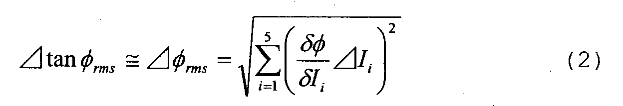
- the measuring wavefront ⁇ is generated from interference fringes I1-I5 that shift the phase by the following equation.
- the interference fringe I1-I5 are intensities of the interference fringes when the diffraction grating of FIG. 7 is shifted respectively per 1/4 pitches.
- FIG. 7 is expanding an imitative view of the optical path of the PDI system. At this time, the following equation is met.
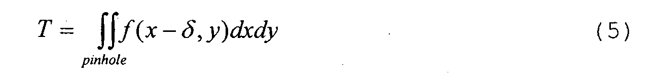
- Transmitting light T of the pinhole 20a is shown by the following equation if the mask drift is ⁇ in the X-direction. However, an integrating range is within the pinhole diameter.
- the equations 5 and 6 provide a relationship between the contrast ⁇ and the mask drift ⁇ .
- f is Gauss function having the mesial magnitude width of 30nm
- the pinhole diameter is 50nm
- the contrast allowance value ⁇ is 0.4
- the mask drift of 55nm is roughly allowed in the ideal condition.
- FIG. 3 a relative positional offset at a condensing point of the light and the pinhole 20a is described as alignment accuracy.
- a condensing point of the target optical system 18 by the 0th order beam of the diffraction grating 14 is positioned to a center of the pinhole 20a in the pinhole mask 20.
- the PDI measurement (step 104) measures five, nine or more sheets of interference fringes using a CCD by moving the lattice shown in FIGS. 4 and 7 per 1/4 or 1/8 lattice interval according to the phase-shift method.
- the contrast decrease caused by the clogging pinhole 20a and the positional offset of the stage 22 is below a permissible value.
- the clogging pinhole 20a and the positional offset of the stage 22 may cause the decreased contrast of the interference fringe as the number of measurements increases.
- the judgment of the contrast (step 106) shifts to step 110 when the contrast of the interference fringe becomes below the permissible value by during the measurement.
- the set permissible value of the contrast depends on the measuring method and the purpose.
- An estimate of the wavefront tilt component calculates a wrapped phase on a pupil from one sheet of interference fringe so as to estimate the wavefront tilt of a single bucket.
- the wavefront tilt can be estimated within a short measuring time by calculating the phase from a single bucket though calculating of the wrapped phase on the pupil from 5 or 9 bucket of interference fringes usually provides high accuracy.
- the wavefront can be obtained by calculating the wrapped phase on the pupil from the interference fringes and by unwrapping the phase.
- the inclination element on this wavefront corresponds to the tilt component.
- the system of FIG. 7 generates a Y tilt Ty of 40 ⁇ and X Tilt Tx of 0 ⁇ . Next, the amount of the relative positional offset is estimated.
- Step 112 moves to step 114, if the mask drift (i.e., or the alignment accuracy) calculated in the step 110 is higher than the permissible value, and moves to step 120 if it is below the permissible value.
- the mask drift i.e., or the alignment accuracy
- the step 114 moves the stage 22 only by the amount of the relative positional offset calculated in the step 110.
- the tilt is reconfirmed (step 116) after the movement and it is confirmed whether the amount of the relative positional offset is below the permissible value (step 118). If it is above the permissible value the step 118 shifts to the step 114. On the other hand, the step 118 shifts to the step 104 so as to measure the interference fringes if the amount is below the permissible value.
- the step 120 is to exchange the pinhole 20a in the second mask 20.
- An exchange of the pinhole may be an exchange of a mask or a movement to another pair of a pinhole and a window in the second mask.
- the measuring system where a relative positional offset of the condensing point and the pinhole mask 20 exists and the pinhole is clogged can efficiently judge the exchange of the pinhole 20a by executing a series of process according to the flowchart of such FIGS. 1 and 3. As a result, the interference fringe with high contrast can be acquired. Moreover, the mis-detection caused because the pinhole 20a is clogged and the shape changes is prevented.
- FIG.5A is a schematic optical path view of the measuring apparatus 30.
- the shape of the first mask 12 and the second mask 20 in the measuring apparatus 30 is different from that of the measuring apparatus 10 of FIG. 4.
- the first mask 31 includes a slit 31a in FIG.5B.
- FIG.5B is a schematic plane view of the first mask 31.
- the second mask 32 includes a slit 32a and a window 32b for measuring light to be detected as shown in FIG. 5C.
- the second mask 32 may arrange some slits in one window as shown in FIG.5D.
- the wavefront shot from the first mask 31 has an element almost equal to an ideal spherical wave about the direction of the slit 31a' s width, that is, direction of a short dimension. Therefore, when the wavefront element of the direction of the slit width is used, the wavefront aberration of the projection optical system 18 can be measured in the LDI interferometer by the same principle as the PDI interferometer. However, because obtained the wavefront aberration naturally is limited to the element of the direction of the slit width, another one slit where the direction of the slit rotated by 90 degrees is necessary to measure the wavefront aberration in the direction of length (direction of long dimension) of the slit. The wavefront aberration of the projection optical system 18 can be measured by synthesizing the wavefront aberration obtained respectively in these slits.
- light generated from the light source condenses to the slit 31a in the first mask 31 according to a condenser apparatus shown in FIG. 5.
- the measuring light after the pinhole 12a is passed forms a standard spherical wave and faces the projection optical system 18.
- the diffraction grating 14 arranged between the 1 St mask 12 and the projection optical system 18 is arranged parallel to a direction perpendicular to the paper surface, divides the measuring light vertically in the paper surface, and turns the light toward an orientation corresponding to the pitch of the diffraction grating.
- the projection optical system 18 condenses each diffraction light into the image surface.
- the 0th order beam of large quantities condenses to the slit 32a of the second mask 32 and the 1st diffracted order beam of small quantities condenses to the window 32b in the light condensed by the projection optical system 18.
- the 0th order beam becomes a wavefront with the same element as a spherical wave that has no aberration in the direction of the slit width by passing the slit 32a at least one of two light that passed the second mask 32.
- the 1st diffracted order beam becomes a wavefront with aberration information of the projection optical system 18 because it passes the window 32b with a big opening from the diffraction limit.
- the 0th order beam and the 1st diffracted order beam form a interference fringe (a wavefront to be detected TW) as well as the case of the PDI after passing the second mask 32, and these beams are observed by the detector 26.
- the aberration in the direction of width of the slit in the projection optical system 18 can be measured from this interference fringe.
- the slit 31a of the first mask 31 and the slit 32a of the second mask 32 is very small, and the wavefront of the light after the slit is shot becomes an ideal spherical wave very near about the element of the direction of width of the slit. Therefore, the absolute value of the aberration of the projection optical system 14 can be guaranteed by high accuracy. High reproducibility can be achieved because the 0th order beam and the 1st diffracted order beam almost pass the same optical path.
- the interference fringe generated by the second mask 32 is detected by the detector 26, and can request the wavefront aberration by the calculation.
- the light passing the slit of the second mask 32 generates an ideal spherical wave to one dimension in the width direction of the slit. Therefore, the wavefront obtained by one measurement is a correct wavefront only in the direction of the slit of a short dimension.
- the wavefront aberration is measured based on the flow of FIG. 2B to obtain the wavefront where the target optical system is correct.
- "Routine A” is executed by using the first slit.
- the wavefront aberration of the projection optical system 18 is acquired by executing "Routine A” using a slit used for the first measurement where the direction is different by 90 degrees in the slit, and by executing the synthesis (step 108) of the wavefront of the first measurement and the wavefront of the second measurement.
- “Routine A” is shown in FIG. 3, the first mask 12 was replaced with the first mask 31 and the second mask 20 was replaced with the second mask 32 in "Routine A" explained in the embodiment of above PDI.
- FIG. 8 is a schematic clog view of the exposure apparatus 40 using the EUV light as exposure light.
- the exposure apparatus of this present invention is not the one limited to the EUV light.
- 41 is an illumination apparatus including the light source
- 42 is a reticle stage
- 44 is a reticle
- the reticle may mean the first mask 12 and a reticle where the circuit pattern of the semiconductor device (semiconductor chip, liquid crystal panel, and CCD etc. such as IC and LSI) is arranged (However, the pinhole 12a is necessary in this case.).
- 18 is a projection optical system that is the target optical system
- 45 is a wafer stage
- 14A is a diffraction grating (optical division means), the diffraction grating may be arranged on a reticle stage side though is on a wafer stage 45 side in FIG. 8.
- the diffraction grating 14A includes the structure similar to the diffraction grating 14 shown in FIG. 4, and two patterns with an orthogonal direction of the lattice.
- 46 is a pattern surface where the pinhole 20a and the window 20b are arranged
- 26 is a detector and 47 is an object to be exposed (i.e. a wafer in this embodiment).
- the pattern surface 46 and the detector 26 are integral structure, being arranged on the wafer stage 45.
- the illumination system 41 illuminates the mask 44
- the diffraction grating 14A divides light of a wavefront where only one direction shot from the pinhole 12a is a sphere via the projection optical system 18
- the 0th order beam injects into the pinhole 20a of the pattern 46
- the 1st diffracted order beam injects into the window 20b
- the detector 26 detects an interference fringe.
- the interference fringe acquired by the detector 26 is obtained, and the phase of the interference fringe is obtained by Moire method by using a calculation means (not shown) because the interference fringe includes a TLT fringe that correspond to a separation angle separation between the 0th order beam and the 1 st order beam.
- the phase of the interference fringe can be obtained by the phase-shift method because a scanning means (not shown) vertically scans the diffraction optical element to an optical axis of the projection optical system18.
- the phase-shift method 16 moves the diffraction grating 14A, and an aberration characteristic within an angle of view of a projection optical system is measured by similarly the aberration measurement in several points within the angle of view of the projection optical system 18. It is a composition in which the aberration measuring function is added easily by using the reflection pattern as a mask in the projection exposure apparatus of this embodiment.
- the exposure apparatus 40 can move plural optical elements (not shown) in the direction of an optical axis and/or the orthogonal direction of an optical axis.
- the exposure apparatus 40 can correct an aberration (especially, five aberrations of Zaidel) of one or more value(s) in the projection optical system by driving one or more optical element(s) based on aberration information obtained by this embodiment of a driving apparatus (not shown) for adjusting an aberration.
- the means for adjusting the aberration of the projection optical system 40 includes not only a movable lens but also well-known factions like a movable mirror (When the optical system is Catadioptoric system and a mirror system.), a tilting parallel monotony, space that can control pressure, or a surface correction by the actuator, etc.
- FIG. 9 is a flowchart for explaining a fabrication of devices (i.e., semiconductor chips such as IC and LSI, LCDs, CCDs, etc.).
- Step 1 circuit design
- Step 2 mask fabrication
- Step 3 wafer preparation
- Step 4 wafer process
- a pretreatment forms actual circuitry on the wafer through photolithography using the mask and wafer.
- Step 5 (assembly), which is also referred to as a posttreatment, forms into a semiconductor chip the wafer formed in Step 4 and includes an assembly step (e.g., dicing, bonding), a packaging step (chip sealing), and the like.
- Step 6 (inspection) performs various tests for the semiconductor device made in Step 5, such as a validity test and a durability test. Through these steps, a semiconductor device is finished and shipped (Step 7).
- FIG. 10 is a detailed flowchart of the wafer process in Step 4 in FIG. 9.
- Step 11 oxidation
- Step 12 CVD
- Step 13 electrode formation
- Step 14 ion implantation
- Step 15 resist process
- Step 16 exposure
- Step 17 development
- Step 18 etching
- Step 19 resist stripping
- the present invention provides the measuring method more highly accurate than the prior art and to be able to measure the wavefront of the target optical system using the interference measuring method, apparatus using interference, exposure method and apparatus using the same, and device fabrication.
Landscapes
- Physics & Mathematics (AREA)
- General Physics & Mathematics (AREA)
- Exposure And Positioning Against Photoresist Photosensitive Materials (AREA)
- Testing Of Optical Devices Or Fibers (AREA)
- Exposure Of Semiconductors, Excluding Electron Or Ion Beam Exposure (AREA)
- Instruments For Measurement Of Length By Optical Means (AREA)
Abstract
Description
Claims (19)
- A measuring method for measuring an interference fringe including the steps of:generating the interference fringe between light that has passed a target optical system, and a reference wave that is generated from part of the light that has passed a mask;determining whether contrast of the interference fringe is higher than a predetermined threshold; andchanging a condition of generating the reference wave when the contrast is below the predetermined threshold.
- A measuring method according to claim 1, wherein the predetermined threshold is 0.4.
- A measuring method according to claim 1, wherein the reference wave is generated as a result of that the part of light transmits through a slit or pinhole in the mask.
- A measuring method according to claim 3, wherein the changing step includes a step of moving the mask.
- A measuring method according to claim 3, wherein the changing step includes a step of calculating a tilt on a wavefront of the optical system.
- A measuring method according to claim 3, wherein the changing step includes a step of exchanging the pinhole or the slit.
- An exposing method including the steps of:wherein the measuring method for measuring an interference fringe including the steps of:calculating a wavefront aberration of a target optical system by using a measuring method;adjusting the optical system based on the wavefront aberration of the calculated optical system; andexposing an object to be exposed with the adjusted optical system;generating the interference fringe between light that has passed a target optical system, and a reference wave that is generated from part of the light that has passed a mask;determining whether contrast of the interference fringe is higher than a predetermined threshold; andchanging a condition of generating the reference wave when the contrast is below the predetermined threshold.
- A measuring apparatus for measuring a wavefront of a target optical system, the measuring apparatus including:a mask for generating a reference wave using part of light from the optical system;a measuring part for measuring an interference fringe between the reference wave and the light;a determining part for determining whether contrast of the interference fringe is higher than a predetermined threshold; anda changing part for changing a condition of generating the reference wave.
- An exposure apparatus for exposing a pattern formed on a mask onto an object to be exposed by using a light beam, the exposure apparatus including:wherein the measuring apparatus includes a mask for generating a reference wave using part of light from the optical system,a projection optical system for projecting the pattern onto the object; anda measuring apparatus for detecting a wavefront aberration of the projection optical system by using the light beam and an interference;
a measuring part for measuring an interference fringe between the reference wave and the light,
a determining part for determining whether contrast of the interference fringe is higher than a predetermined threshold, and
a changing part for changing a condition of generating the reference wave. - An exposure apparatus according to claim 9, wherein the light is an extreme ultraviolet having a wavelength of 20nm or less.
- A device fabrication method including the steps of:wherein the exposure apparatus for exposing a pattern formed on a mask onto an object to be exposed by using a light beam, the exposure apparatus comprises:exposing an object using an exposure apparatus; andperforming a development process for the object exposed,wherein the measuring apparatus includes a mask for generating a reference wave using part of light from the optical system,a projection optical system for projecting the pattern onto the object; anda measuring apparatus for detecting a wavefront aberration of the projection optical system by using the light beam and an interference;
a measuring part for measuring an interference fringe between the reference wave and the light,
a determining part for determining whether contrast of the interference fringe is higher than a predetermined threshold, and
a changing part for changing a condition of generating the reference wave,
the method further comprising one or more further steps for making a device using at least a part of the developed object. - A method of measuring an optical aberration of an optical system comprising:characterised by:(a) generating an optical wavefront;(b) passing the optical wavefront through the optical system (18);(c) passing the optical wavefront through a mask (20); and(d) analysing the light that has passed through the optical system and the mask to derive a measure of the optical aberration of the optical system,(e) analysing the light that has passed through the mask to determine whether the mask is at least one of (i) misaligned relative to the optical wavefront and (ii) at least partially obstructed by a contaminant;
and, if it is so determined,(f) taking remedial action. - A method according to claim 12 in which the step (a) of generating an optical wavefront comprises passing light through a point or a slit to form a wavefront which is arcuate in at least one direction.
- A method according to claim 12 or claim 13 which comprises:(g) diffracting the optical wavefront before or after it is passed through the optical system.
- A method according to claim 14 in which the mask comprises a point or a slit for passing zero-order diffracted light and a window for passing light of a non-zero order of diffraction.
- A method according to claim 15 in which the mask comprises a plurality of said points or slits and a plurality of said windows, whereby the mask is usable at a plurality of positions relative to the optical wavefront.
- A method according to any one of claims 12 to 16 in which the remedial action comprises improving alignment by moving the mask, in the case that misalignment is determined.
- A method according to any one of claims 12 to 17 in which the remedial action comprises moving the mask to align a different part of it with the optical wavefront in the case that at least a partial obstruction by a contaminant is determined.
- A method according to any one of claims 12 to 17 in which the remedial action comprises exchanging the mask in the case that at least partial obstruction by a contaminant is determined.
Applications Claiming Priority (2)
| Application Number | Priority Date | Filing Date | Title |
|---|---|---|---|
| JP2003399216A JP4408040B2 (en) | 2003-11-28 | 2003-11-28 | Measurement method and apparatus using interference, exposure method and apparatus using the same, and device manufacturing method |
| JP2003399216 | 2003-11-28 |
Publications (2)
| Publication Number | Publication Date |
|---|---|
| EP1536289A2 true EP1536289A2 (en) | 2005-06-01 |
| EP1536289A3 EP1536289A3 (en) | 2006-05-17 |
Family
ID=34463880
Family Applications (1)
| Application Number | Title | Priority Date | Filing Date |
|---|---|---|---|
| EP04257382A Withdrawn EP1536289A3 (en) | 2003-11-28 | 2004-11-29 | Measuring method using interference |
Country Status (3)
| Country | Link |
|---|---|
| US (1) | US7283252B2 (en) |
| EP (1) | EP1536289A3 (en) |
| JP (1) | JP4408040B2 (en) |
Cited By (3)
| Publication number | Priority date | Publication date | Assignee | Title |
|---|---|---|---|---|
| EP1568976A1 (en) * | 2004-02-27 | 2005-08-31 | Canon Kabushiki Kaisha | Exposure apparatus mounted with measuring apparatus |
| EP2098910A1 (en) | 2008-03-07 | 2009-09-09 | Canon Kabushiki Kaisha | Wavefront aberration measuring apparatus, wavefront aberration measuring method, exposure apparatus, and device manufacturing method |
| CN103267629A (en) * | 2013-06-25 | 2013-08-28 | 中国科学院上海光学精密机械研究所 | Point-diffraction interference wave aberration measuring instrument |
Families Citing this family (15)
| Publication number | Priority date | Publication date | Assignee | Title |
|---|---|---|---|---|
| JP4590181B2 (en) * | 2003-11-28 | 2010-12-01 | キヤノン株式会社 | Measuring method and apparatus, exposure apparatus, and device manufacturing method |
| JP4630611B2 (en) | 2004-09-01 | 2011-02-09 | キヤノン株式会社 | Exposure apparatus and method provided with interferometer, and device manufacturing method |
| JP4666982B2 (en) * | 2004-09-02 | 2011-04-06 | キヤノン株式会社 | Optical characteristic measuring apparatus, exposure apparatus, and device manufacturing method |
| JP2006228930A (en) | 2005-02-17 | 2006-08-31 | Canon Inc | Measuring apparatus and exposure apparatus equipped with the same |
| JP2006332586A (en) * | 2005-04-25 | 2006-12-07 | Canon Inc | Measuring apparatus, exposure apparatus and method, and device manufacturing method |
| JP2006324311A (en) * | 2005-05-17 | 2006-11-30 | Canon Inc | Wavefront aberration measuring apparatus and exposure apparatus having the same |
| JP2007035709A (en) * | 2005-07-22 | 2007-02-08 | Canon Inc | Exposure apparatus and device manufacturing method using the same |
| JP2007180152A (en) * | 2005-12-27 | 2007-07-12 | Canon Inc | Measuring method and apparatus, exposure apparatus, and device manufacturing method |
| JP2007234685A (en) * | 2006-02-28 | 2007-09-13 | Canon Inc | Measuring apparatus, exposure apparatus having the measuring apparatus, and device manufacturing method |
| US7633630B2 (en) * | 2006-08-09 | 2009-12-15 | Northrop Grumman Corporation | Image amplifying, servo-loop controlled, point diffraction interometer |
| DE102008029970A1 (en) | 2008-06-26 | 2009-12-31 | Carl Zeiss Smt Ag | Projection exposure apparatus for microlithography and method for monitoring a lateral imaging stability |
| JP5522944B2 (en) * | 2009-01-09 | 2014-06-18 | キヤノン株式会社 | Measuring apparatus, measuring method and exposure apparatus |
| JP5503193B2 (en) * | 2009-06-08 | 2014-05-28 | キヤノン株式会社 | Wavefront aberration measuring apparatus, exposure apparatus, and device manufacturing method |
| NL2021357A (en) * | 2018-01-31 | 2018-08-16 | Asml Netherlands Bv | Two-dimensional diffraction grating |
| CN120259898B (en) * | 2025-06-06 | 2025-08-08 | 江西通慧科技集团股份有限公司 | Bridge crack sub-pixel recognition method and system based on moiré phase unwrapping |
Family Cites Families (12)
| Publication number | Priority date | Publication date | Assignee | Title |
|---|---|---|---|---|
| JPS5764139A (en) | 1980-10-08 | 1982-04-19 | Nippon Kogaku Kk <Nikon> | Interferometer |
| US4832489A (en) * | 1986-03-19 | 1989-05-23 | Wyko Corporation | Two-wavelength phase-shifting interferometer and method |
| EP0577088B2 (en) * | 1992-06-30 | 2010-10-20 | Canon Kabushiki Kaisha | Displacement information detection apparatus |
| US5457533A (en) * | 1994-06-10 | 1995-10-10 | Wilcken; Stephen K. | Point-diffraction interferometer utilizing separate reference and signal beam paths |
| US5835217A (en) * | 1997-02-28 | 1998-11-10 | The Regents Of The University Of California | Phase-shifting point diffraction interferometer |
| JP2000097666A (en) | 1998-09-22 | 2000-04-07 | Nikon Corp | Surface shape measuring interferometer, wavefront aberration measuring device, method for manufacturing projection optical system using the interferometer and the wavefront aberration measuring device, and method for calibrating the interferometer |
| US6312373B1 (en) * | 1998-09-22 | 2001-11-06 | Nikon Corporation | Method of manufacturing an optical system |
| US6195169B1 (en) * | 1998-10-21 | 2001-02-27 | The Regents Of The University Of California | Phase-shifting point diffraction interferometer grating designs |
| US6360012B1 (en) | 1999-06-25 | 2002-03-19 | Svg Lithography Systems, Inc. | In situ projection optic metrology method and apparatus |
| US6151115A (en) * | 1999-07-26 | 2000-11-21 | Naulleau; Patrick | Phase-shifting point diffraction interferometer focus-aid enhanced mask |
| US6559952B1 (en) * | 2000-05-11 | 2003-05-06 | The Regents Of The University Of California | System for interferometric distortion measurements that define an optical path |
| US6573997B1 (en) * | 2000-07-17 | 2003-06-03 | The Regents Of California | Hybrid shearing and phase-shifting point diffraction interferometer |
-
2003
- 2003-11-28 JP JP2003399216A patent/JP4408040B2/en not_active Expired - Fee Related
-
2004
- 2004-11-26 US US10/996,381 patent/US7283252B2/en not_active Expired - Fee Related
- 2004-11-29 EP EP04257382A patent/EP1536289A3/en not_active Withdrawn
Cited By (6)
| Publication number | Priority date | Publication date | Assignee | Title |
|---|---|---|---|---|
| EP1568976A1 (en) * | 2004-02-27 | 2005-08-31 | Canon Kabushiki Kaisha | Exposure apparatus mounted with measuring apparatus |
| US7619748B2 (en) | 2004-02-27 | 2009-11-17 | Canon Kabushiki Kaisha | Exposure apparatus mounted with measuring apparatus |
| EP2098910A1 (en) | 2008-03-07 | 2009-09-09 | Canon Kabushiki Kaisha | Wavefront aberration measuring apparatus, wavefront aberration measuring method, exposure apparatus, and device manufacturing method |
| US8373866B2 (en) | 2008-03-07 | 2013-02-12 | Canon Kabushiki Kaisha | Wavefront aberration measuring apparatus, wavefront aberration measuring method, exposure apparatus, and device manufacturing method |
| CN103267629A (en) * | 2013-06-25 | 2013-08-28 | 中国科学院上海光学精密机械研究所 | Point-diffraction interference wave aberration measuring instrument |
| CN103267629B (en) * | 2013-06-25 | 2015-04-15 | 中国科学院上海光学精密机械研究所 | Point-diffraction interference wave aberration measuring instrument and measuring method thereof |
Also Published As
| Publication number | Publication date |
|---|---|
| JP4408040B2 (en) | 2010-02-03 |
| US7283252B2 (en) | 2007-10-16 |
| US20050117171A1 (en) | 2005-06-02 |
| EP1536289A3 (en) | 2006-05-17 |
| JP2005156506A (en) | 2005-06-16 |
Similar Documents
| Publication | Publication Date | Title |
|---|---|---|
| EP1536289A2 (en) | Measuring method using interference | |
| US7880880B2 (en) | Alignment systems and methods for lithographic systems | |
| CN108398856B (en) | Metrology method and apparatus, lithographic system and device manufacturing method | |
| US6285033B1 (en) | Positional deviation detecting method and device manufacturing method using the same | |
| US8208121B2 (en) | Alignment mark and a method of aligning a substrate comprising such an alignment mark | |
| US7609390B2 (en) | Measurement method and apparatus, exposure apparatus | |
| US8472009B2 (en) | Exposure apparatus and device manufacturing method | |
| US6421124B1 (en) | Position detecting system and device manufacturing method using the same | |
| US7576858B2 (en) | Position detecting method | |
| KR20060014063A (en) | Position information measuring method and apparatus, and exposure method and apparatus | |
| US20050117170A1 (en) | Measuring method and apparatus using shearing interferometry, exposure method and apparatus using the same, and device manufacturing method | |
| CN110088683B (en) | Method for monitoring characteristics of illumination from a metrology device | |
| EP1400854A2 (en) | Alignment systems and methods for lithographic systems | |
| JP4403880B2 (en) | Position detection apparatus, position detection method, exposure apparatus, and exposure method | |
| JPH09270382A (en) | Projection exposure apparatus and semiconductor device manufacturing method using the same | |
| US20100177290A1 (en) | Optical characteristic measuring method, optical characteristic adjusting method, exposure apparatus, exposing method, and exposure apparatus manufacturing method | |
| JPH0922868A (en) | Projection exposure apparatus and semiconductor device manufacturing method using the same | |
| JPH09115822A (en) | Projection exposure apparatus and semiconductor device manufacturing method using the same | |
| JPH08288208A (en) | Projection exposure apparatus and semiconductor device manufacturing method using the same | |
| HK1136691A (en) | Optical characteristic measurement method, optical characteristic adjusting method, exposure device, exposure method, and exposure device manufacturing method |
Legal Events
| Date | Code | Title | Description |
|---|---|---|---|
| PUAI | Public reference made under article 153(3) epc to a published international application that has entered the european phase |
Free format text: ORIGINAL CODE: 0009012 |
|
| AK | Designated contracting states |
Kind code of ref document: A2 Designated state(s): AT BE BG CH CY CZ DE DK EE ES FI FR GB GR HU IE IS IT LI LU MC NL PL PT RO SE SI SK TR |
|
| AX | Request for extension of the european patent |
Extension state: AL HR LT LV MK YU |
|
| PUAL | Search report despatched |
Free format text: ORIGINAL CODE: 0009013 |
|
| AK | Designated contracting states |
Kind code of ref document: A3 Designated state(s): AT BE BG CH CY CZ DE DK EE ES FI FR GB GR HU IE IS IT LI LU MC NL PL PT RO SE SI SK TR |
|
| AX | Request for extension of the european patent |
Extension state: AL HR LT LV MK YU |
|
| 17P | Request for examination filed |
Effective date: 20061117 |
|
| AKX | Designation fees paid |
Designated state(s): DE ES FR GB IT NL |
|
| 17Q | First examination report despatched |
Effective date: 20070207 |
|
| STAA | Information on the status of an ep patent application or granted ep patent |
Free format text: STATUS: THE APPLICATION HAS BEEN WITHDRAWN |
|
| 18W | Application withdrawn |
Effective date: 20110516 |