CN108398856B - Metrology method and apparatus, lithographic system and device manufacturing method - Google Patents
Metrology method and apparatus, lithographic system and device manufacturing method Download PDFInfo
- Publication number
- CN108398856B CN108398856B CN201810061591.1A CN201810061591A CN108398856B CN 108398856 B CN108398856 B CN 108398856B CN 201810061591 A CN201810061591 A CN 201810061591A CN 108398856 B CN108398856 B CN 108398856B
- Authority
- CN
- China
- Prior art keywords
- asymmetry
- overlay
- target structure
- target
- bias
- Prior art date
- Legal status (The legal status is an assumption and is not a legal conclusion. Google has not performed a legal analysis and makes no representation as to the accuracy of the status listed.)
- Active
Links
- 238000000034 method Methods 0.000 title claims abstract description 91
- 238000004519 manufacturing process Methods 0.000 title description 9
- 238000005259 measurement Methods 0.000 claims abstract description 109
- 239000000758 substrate Substances 0.000 claims abstract description 84
- 238000005286 illumination Methods 0.000 claims abstract description 59
- 230000008569 process Effects 0.000 claims abstract description 28
- 238000012417 linear regression Methods 0.000 claims abstract description 22
- 238000007689 inspection Methods 0.000 claims abstract description 20
- 230000015572 biosynthetic process Effects 0.000 claims abstract description 6
- 238000000611 regression analysis Methods 0.000 claims abstract description 6
- 230000005855 radiation Effects 0.000 claims description 72
- 230000003287 optical effect Effects 0.000 claims description 22
- 230000000737 periodic effect Effects 0.000 claims description 17
- 238000012937 correction Methods 0.000 claims description 10
- 238000000059 patterning Methods 0.000 description 39
- 210000001747 pupil Anatomy 0.000 description 22
- 238000003384 imaging method Methods 0.000 description 13
- 239000010410 layer Substances 0.000 description 10
- 230000006870 function Effects 0.000 description 9
- 238000004458 analytical method Methods 0.000 description 8
- 230000000694 effects Effects 0.000 description 7
- 238000001459 lithography Methods 0.000 description 7
- 230000010287 polarization Effects 0.000 description 7
- 238000012545 processing Methods 0.000 description 7
- 239000002131 composite material Substances 0.000 description 6
- 238000010586 diagram Methods 0.000 description 6
- 230000008901 benefit Effects 0.000 description 5
- 238000004590 computer program Methods 0.000 description 5
- 239000007788 liquid Substances 0.000 description 5
- 230000035945 sensitivity Effects 0.000 description 5
- 238000001228 spectrum Methods 0.000 description 5
- 238000009826 distribution Methods 0.000 description 4
- 238000007654 immersion Methods 0.000 description 4
- 102100029469 WD repeat and HMG-box DNA-binding protein 1 Human genes 0.000 description 3
- 101710097421 WD repeat and HMG-box DNA-binding protein 1 Proteins 0.000 description 3
- 230000001419 dependent effect Effects 0.000 description 3
- 239000011159 matrix material Substances 0.000 description 3
- 239000000203 mixture Substances 0.000 description 3
- 238000005457 optimization Methods 0.000 description 3
- 239000000047 product Substances 0.000 description 3
- 239000004065 semiconductor Substances 0.000 description 3
- 230000006978 adaptation Effects 0.000 description 2
- 238000013459 approach Methods 0.000 description 2
- 238000003491 array Methods 0.000 description 2
- 238000013461 design Methods 0.000 description 2
- 230000009977 dual effect Effects 0.000 description 2
- 230000005670 electromagnetic radiation Effects 0.000 description 2
- 238000000691 measurement method Methods 0.000 description 2
- 238000012986 modification Methods 0.000 description 2
- 230000004048 modification Effects 0.000 description 2
- 230000010363 phase shift Effects 0.000 description 2
- 238000000206 photolithography Methods 0.000 description 2
- 230000003068 static effect Effects 0.000 description 2
- 238000003860 storage Methods 0.000 description 2
- 238000012876 topography Methods 0.000 description 2
- 238000012546 transfer Methods 0.000 description 2
- 238000012935 Averaging Methods 0.000 description 1
- XUIMIQQOPSSXEZ-UHFFFAOYSA-N Silicon Chemical compound [Si] XUIMIQQOPSSXEZ-UHFFFAOYSA-N 0.000 description 1
- 230000002238 attenuated effect Effects 0.000 description 1
- 239000006227 byproduct Substances 0.000 description 1
- 238000004364 calculation method Methods 0.000 description 1
- 239000003086 colorant Substances 0.000 description 1
- 239000000470 constituent Substances 0.000 description 1
- 238000007796 conventional method Methods 0.000 description 1
- 238000001918 dark-field optical micrograph Methods 0.000 description 1
- 238000013479 data entry Methods 0.000 description 1
- 238000013500 data storage Methods 0.000 description 1
- 238000001514 detection method Methods 0.000 description 1
- 238000011161 development Methods 0.000 description 1
- 230000018109 developmental process Effects 0.000 description 1
- 238000010894 electron beam technology Methods 0.000 description 1
- 238000005516 engineering process Methods 0.000 description 1
- 238000000605 extraction Methods 0.000 description 1
- 238000001914 filtration Methods 0.000 description 1
- 230000006872 improvement Effects 0.000 description 1
- 238000010884 ion-beam technique Methods 0.000 description 1
- 239000002346 layers by function Substances 0.000 description 1
- 239000000463 material Substances 0.000 description 1
- 230000007246 mechanism Effects 0.000 description 1
- QSHDDOUJBYECFT-UHFFFAOYSA-N mercury Chemical compound [Hg] QSHDDOUJBYECFT-UHFFFAOYSA-N 0.000 description 1
- 229910052753 mercury Inorganic materials 0.000 description 1
- 239000002245 particle Substances 0.000 description 1
- 238000003909 pattern recognition Methods 0.000 description 1
- 238000005498 polishing Methods 0.000 description 1
- 238000000513 principal component analysis Methods 0.000 description 1
- 238000004886 process control Methods 0.000 description 1
- 230000000644 propagated effect Effects 0.000 description 1
- 230000009467 reduction Effects 0.000 description 1
- 238000010187 selection method Methods 0.000 description 1
- 238000007493 shaping process Methods 0.000 description 1
- 229910052710 silicon Inorganic materials 0.000 description 1
- 239000010703 silicon Substances 0.000 description 1
- 239000000126 substance Substances 0.000 description 1
- 238000012360 testing method Methods 0.000 description 1
- 238000012795 verification Methods 0.000 description 1
- XLYOFNOQVPJJNP-UHFFFAOYSA-N water Substances O XLYOFNOQVPJJNP-UHFFFAOYSA-N 0.000 description 1
- 229910052724 xenon Inorganic materials 0.000 description 1
- FHNFHKCVQCLJFQ-UHFFFAOYSA-N xenon atom Chemical compound [Xe] FHNFHKCVQCLJFQ-UHFFFAOYSA-N 0.000 description 1
Images


Classifications
-
- G—PHYSICS
- G03—PHOTOGRAPHY; CINEMATOGRAPHY; ANALOGOUS TECHNIQUES USING WAVES OTHER THAN OPTICAL WAVES; ELECTROGRAPHY; HOLOGRAPHY
- G03F—PHOTOMECHANICAL PRODUCTION OF TEXTURED OR PATTERNED SURFACES, e.g. FOR PRINTING, FOR PROCESSING OF SEMICONDUCTOR DEVICES; MATERIALS THEREFOR; ORIGINALS THEREFOR; APPARATUS SPECIALLY ADAPTED THEREFOR
- G03F7/00—Photomechanical, e.g. photolithographic, production of textured or patterned surfaces, e.g. printing surfaces; Materials therefor, e.g. comprising photoresists; Apparatus specially adapted therefor
- G03F7/70—Microphotolithographic exposure; Apparatus therefor
- G03F7/70483—Information management; Active and passive control; Testing; Wafer monitoring, e.g. pattern monitoring
- G03F7/70605—Workpiece metrology
- G03F7/70616—Monitoring the printed patterns
- G03F7/70633—Overlay, i.e. relative alignment between patterns printed by separate exposures in different layers, or in the same layer in multiple exposures or stitching
-
- G—PHYSICS
- G03—PHOTOGRAPHY; CINEMATOGRAPHY; ANALOGOUS TECHNIQUES USING WAVES OTHER THAN OPTICAL WAVES; ELECTROGRAPHY; HOLOGRAPHY
- G03F—PHOTOMECHANICAL PRODUCTION OF TEXTURED OR PATTERNED SURFACES, e.g. FOR PRINTING, FOR PROCESSING OF SEMICONDUCTOR DEVICES; MATERIALS THEREFOR; ORIGINALS THEREFOR; APPARATUS SPECIALLY ADAPTED THEREFOR
- G03F1/00—Originals for photomechanical production of textured or patterned surfaces, e.g., masks, photo-masks, reticles; Mask blanks or pellicles therefor; Containers specially adapted therefor; Preparation thereof
- G03F1/68—Preparation processes not covered by groups G03F1/20 - G03F1/50
- G03F1/72—Repair or correction of mask defects
-
- G—PHYSICS
- G03—PHOTOGRAPHY; CINEMATOGRAPHY; ANALOGOUS TECHNIQUES USING WAVES OTHER THAN OPTICAL WAVES; ELECTROGRAPHY; HOLOGRAPHY
- G03F—PHOTOMECHANICAL PRODUCTION OF TEXTURED OR PATTERNED SURFACES, e.g. FOR PRINTING, FOR PROCESSING OF SEMICONDUCTOR DEVICES; MATERIALS THEREFOR; ORIGINALS THEREFOR; APPARATUS SPECIALLY ADAPTED THEREFOR
- G03F7/00—Photomechanical, e.g. photolithographic, production of textured or patterned surfaces, e.g. printing surfaces; Materials therefor, e.g. comprising photoresists; Apparatus specially adapted therefor
- G03F7/70—Microphotolithographic exposure; Apparatus therefor
- G03F7/70483—Information management; Active and passive control; Testing; Wafer monitoring, e.g. pattern monitoring
- G03F7/70491—Information management, e.g. software; Active and passive control, e.g. details of controlling exposure processes or exposure tool monitoring processes
- G03F7/70508—Data handling in all parts of the microlithographic apparatus, e.g. handling pattern data for addressable masks or data transfer to or from different components within the exposure apparatus
-
- G—PHYSICS
- G03—PHOTOGRAPHY; CINEMATOGRAPHY; ANALOGOUS TECHNIQUES USING WAVES OTHER THAN OPTICAL WAVES; ELECTROGRAPHY; HOLOGRAPHY
- G03F—PHOTOMECHANICAL PRODUCTION OF TEXTURED OR PATTERNED SURFACES, e.g. FOR PRINTING, FOR PROCESSING OF SEMICONDUCTOR DEVICES; MATERIALS THEREFOR; ORIGINALS THEREFOR; APPARATUS SPECIALLY ADAPTED THEREFOR
- G03F7/00—Photomechanical, e.g. photolithographic, production of textured or patterned surfaces, e.g. printing surfaces; Materials therefor, e.g. comprising photoresists; Apparatus specially adapted therefor
- G03F7/70—Microphotolithographic exposure; Apparatus therefor
- G03F7/70483—Information management; Active and passive control; Testing; Wafer monitoring, e.g. pattern monitoring
- G03F7/70605—Workpiece metrology
- G03F7/706835—Metrology information management or control
- G03F7/706839—Modelling, e.g. modelling scattering or solving inverse problems
-
- G—PHYSICS
- G03—PHOTOGRAPHY; CINEMATOGRAPHY; ANALOGOUS TECHNIQUES USING WAVES OTHER THAN OPTICAL WAVES; ELECTROGRAPHY; HOLOGRAPHY
- G03F—PHOTOMECHANICAL PRODUCTION OF TEXTURED OR PATTERNED SURFACES, e.g. FOR PRINTING, FOR PROCESSING OF SEMICONDUCTOR DEVICES; MATERIALS THEREFOR; ORIGINALS THEREFOR; APPARATUS SPECIALLY ADAPTED THEREFOR
- G03F7/00—Photomechanical, e.g. photolithographic, production of textured or patterned surfaces, e.g. printing surfaces; Materials therefor, e.g. comprising photoresists; Apparatus specially adapted therefor
- G03F7/70—Microphotolithographic exposure; Apparatus therefor
- G03F7/70483—Information management; Active and passive control; Testing; Wafer monitoring, e.g. pattern monitoring
- G03F7/70605—Workpiece metrology
- G03F7/706843—Metrology apparatus
-
- H—ELECTRICITY
- H01—ELECTRIC ELEMENTS
- H01L—SEMICONDUCTOR DEVICES NOT COVERED BY CLASS H10
- H01L21/00—Processes or apparatus adapted for the manufacture or treatment of semiconductor or solid state devices or of parts thereof
- H01L21/02—Manufacture or treatment of semiconductor devices or of parts thereof
- H01L21/027—Making masks on semiconductor bodies for further photolithographic processing not provided for in group H01L21/18 or H01L21/34
- H01L21/0271—Making masks on semiconductor bodies for further photolithographic processing not provided for in group H01L21/18 or H01L21/34 comprising organic layers
- H01L21/0273—Making masks on semiconductor bodies for further photolithographic processing not provided for in group H01L21/18 or H01L21/34 comprising organic layers characterised by the treatment of photoresist layers
- H01L21/0274—Photolithographic processes
-
- H—ELECTRICITY
- H01—ELECTRIC ELEMENTS
- H01L—SEMICONDUCTOR DEVICES NOT COVERED BY CLASS H10
- H01L22/00—Testing or measuring during manufacture or treatment; Reliability measurements, i.e. testing of parts without further processing to modify the parts as such; Structural arrangements therefor
- H01L22/10—Measuring as part of the manufacturing process
- H01L22/12—Measuring as part of the manufacturing process for structural parameters, e.g. thickness, line width, refractive index, temperature, warp, bond strength, defects, optical inspection, electrical measurement of structural dimensions, metallurgic measurement of diffusions
-
- H—ELECTRICITY
- H01—ELECTRIC ELEMENTS
- H01L—SEMICONDUCTOR DEVICES NOT COVERED BY CLASS H10
- H01L22/00—Testing or measuring during manufacture or treatment; Reliability measurements, i.e. testing of parts without further processing to modify the parts as such; Structural arrangements therefor
- H01L22/30—Structural arrangements specially adapted for testing or measuring during manufacture or treatment, or specially adapted for reliability measurements
Landscapes
- Engineering & Computer Science (AREA)
- Physics & Mathematics (AREA)
- General Physics & Mathematics (AREA)
- Manufacturing & Machinery (AREA)
- Computer Hardware Design (AREA)
- Microelectronics & Electronic Packaging (AREA)
- Power Engineering (AREA)
- Condensed Matter Physics & Semiconductors (AREA)
- Exposure And Positioning Against Photoresist Photosensitive Materials (AREA)
- Length Measuring Devices By Optical Means (AREA)
- Container, Conveyance, Adherence, Positioning, Of Wafer (AREA)
Abstract
A method of measuring a parameter of a lithographic process and a related inspection apparatus are disclosed. The method comprises the following steps: measuring at least two target structures on a substrate using a plurality of different illumination conditions, the target structures having intentional overlay biases; an asymmetry measurement is obtained for each target structure that represents an overall asymmetry that includes contributions due to (i) intentional overlay bias, (ii) overlay error during formation of the target structure, and (iii) any feature asymmetry. Regression analysis of the asymmetry measurement data is performed by fitting a linear regression model, which is not necessarily fitted to pass through the origin of the planar representation, to the planar representation of the asymmetry measurement for one target structure versus the other target structure. The overlay error may then be determined from the gradient described by the linear regression model.
Description
This application is a divisional application of a patent application having an application date of 2014, month 07, 18, application number of 201480044257.5, entitled "metrology method and apparatus, lithographic system, and device manufacturing method".
Cross Reference to Related Applications
This application claims the benefit of U.S. provisional application 61/863,150 filed on 7/8 in 2013 and U.S. provisional application 61/975,312 filed on 4/4 in 2014, and is incorporated herein by reference in its entirety.
Technical Field
The present invention relates to metrology methods and apparatus useful, for example, in the manufacture of devices by lithographic techniques and to methods of manufacturing devices using lithographic techniques.
Background
A lithographic apparatus is a machine that applies a desired pattern onto a substrate, usually onto a target portion of the substrate. Lithographic apparatus can be used, for example, in the manufacture of Integrated Circuits (ICs). In such cases, a patterning device, which is alternatively referred to as a mask or a reticle, may be used to generate a circuit pattern to be formed on an individual layer of the IC. The pattern can be transferred onto a target portion (e.g., comprising part of, one, or more dies) on a substrate (e.g., a silicon wafer). Typically, the transfer of the pattern is performed by imaging the pattern onto a layer of radiation-sensitive material (resist) provided on the substrate. Typically, a single substrate will contain a network of adjacent target portions that are successively patterned. The known lithographic apparatus comprises: so-called steppers, in which each target portion is irradiated by exposing an entire pattern onto the target portion at one time; and so-called scanners, in which each target portion is irradiated by scanning the pattern through a radiation beam in a given direction (the "scanning" -direction) while synchronously scanning the substrate parallel or anti-parallel to this direction. The pattern may also be transferred from the patterning device to the substrate by imprinting the pattern onto the substrate.
In lithographic processes, it is often desirable to perform measurements on the resulting structure, for example for process control and verification. Various tools for making such measurements are known, including scanning electron microscopes, which are often used to measure Critical Dimension (CD), and specialized tools for measuring overlay (the accuracy of alignment of two layers in a device). Recently, various forms of scatterometers have been developed for use in the field of lithography. These devices direct a beam of radiation onto the target and measure one or more properties of the scattered radiation (e.g., intensity at a single reflection angle as a function of wavelength; intensity at one or more wavelengths as a function of reflection angle; or polarization as a function of reflection angle) to obtain a "spectrum" from which a property of interest of the target can be determined. The determination of the property of interest may be performed by various techniques: the target structure is reconstructed, for example, by iterative methods (e.g., rigorous coupled wave analysis or finite element methods), library search, and principal component analysis.
The target used by some scatterometers is a relatively large (e.g., 40 μm by 40 μm) grating, and the measurement beam generates a spot that is smaller than the grating (i.e., the grating is under-filled). This simplifies the mathematical reconstruction of the object, as it can be seen as infinite. However, in order to reduce the size of the targets, for example to 10 μm x 10 μm or less, for example so that they can be located in product features rather than in scribe lines, it has been proposed that the gratings be made smaller than the measurement spot (i.e. the gratings are overfilled). Typically, such targets are measured using dark field scatterometry, in which the zeroth diffraction order (corresponding to specular reflection) is blocked and only the higher diffraction orders are processed. Diffraction-based overlay using dark-field detection of diffraction orders enables overlay measurements on smaller targets. These targets are smaller than the illumination spot and may be surrounded by product structures on the wafer. Multiple targets can be measured in one image.
In known metrology techniques, the results of the overlay measurements are obtained independently by rotating the target or changing the illumination or imaging mode to obtain-1stDiffraction order sum +1stThe intensity of the diffraction order is obtained by measuring the target twice under certain conditions. Comparing these intensities for a given grating can provide a measure of the asymmetry in the grating, and the asymmetry in the overlapping grating can be used as an indicator of the overlay error.
While known dark-field image-based overlay measurements are fast and computationally simple (once calibrated), they rely on the following assumptions: the overlap is caused only by the asymmetry of the target structure. Any other degree of asymmetry in the stack, e.g. features in one or both of the overlapping gratingsAlso results in 1stAsymmetry of the stages. This characteristic asymmetry has no clear relationship to overlay, but interferes with the overlay measurement, giving inaccurate overlay results. The asymmetry in the bottom grating in the overlaid grating is a common form of feature asymmetry. Which may originate, for example, from wafer processing steps performed after the bottom grating is initially formed, such as Chemical Mechanical Polishing (CMP).
The person skilled in the art therefore has to choose between, on the one hand, a simple and fast measurement procedure which gives an overlapping measurement but which leads to errors in the presence of other causes of asymmetry; on the other hand, more conventional techniques, which are computationally intensive and often require multiple measurements for large, under-filled gratings to avoid interference of the pupil image with signal contributions from the environment of overlapping gratings, would prevent reconstruction based on this pupil image.
Disclosure of Invention
Accordingly, it is desirable to achieve more robust overlay measurements of and/or to distinguish the contribution to target structure asymmetry caused by feature asymmetry from the contribution caused by overlay (including bias).
A first aspect provides a method of measuring a parameter of a lithographic process, the method comprising: (ii) (a) target structures illuminated on the substrate and detecting radiation scattered by each target structure to obtain an asymmetry measurement for each target structure indicative of an overall asymmetry, the target structures comprising at least a first target structure comprising overlapping periodic structures with a first intentional overlay bias and a second target structure comprising overlapping periodic structures with a second intentional overlay bias, the overall asymmetry comprising contributions due to (i) intentional overlay bias in the target structures, (ii) overlay errors in a lithographic process during formation of the target structures and (iii) feature asymmetries in one or more of the periodic structures; (b) repeating step (a) for a plurality of different illumination conditions; (c) performing a regression analysis on the asymmetry measurement data obtained in step (b) by fitting a linear regression model, which is not necessarily fitted to an origin represented by a plane, to the plane representation of asymmetry measurements for the first target structure versus asymmetry measurements for the second target structure; and (d) determining an overlay error from the gradient described by the linear regression model.
Another aspect provides an inspection apparatus for measuring a parameter of a lithographic process, the inspection apparatus comprising: a support for a substrate having a plurality of target structures thereon, the target structures including at least a first target structure and a second target structure, the first target structure including an overlapping periodic structure having a first intentional overlay bias, the second target structure including an overlapping periodic structure having a second intentional overlay bias; an optical system operable to illuminate the targets and to detect radiation scattered by each target to obtain, for each target structure and for a plurality of different illumination conditions, an asymmetry measurement representing an overall asymmetry comprising contributions due to (i) intentional overlay bias in the target structure, (ii) overlay error in a lithographic process during formation of the target structure, and (iii) feature asymmetry in one or more of the periodic structures; a processor arranged to: performing a regression analysis on the asymmetry measurement data by fitting a linear regression model, which is not necessarily fitted to an origin represented by a plane, to the plane representation of the asymmetry measurement for the first target structure versus the plane representation of the asymmetry measurement for the second target structure; and determining an overlay error from the gradient described by the linear regression model.
Yet another aspect provides a computer program product comprising machine readable instructions for causing a processor to perform the processing steps (c) and (d) of the method according to the first aspect described above on asymmetry data obtained by: illuminating target structures on a substrate under a plurality of different illumination conditions, the target structures including at least a first target structure and a second target structure, the first target structure including overlapping periodic structures with a first intentional overlay bias, the second target structure including overlapping periodic structures with a second intentional overlay bias; and detecting radiation scattered by each target structure to obtain, for each target structure, an asymmetry measurement representing an overall asymmetry comprising contributions due to (i) intentional overlay bias in the target structure, (ii) overlay error in a lithographic process during formation of the target structure, and (iii) feature asymmetry in one or more of the periodic structures.
Yet another aspect provides a lithographic apparatus comprising an inspection apparatus as described above, the inspection apparatus being operable to: applying a device pattern to a series of substrates using a lithographic process; applying a target structure to one or more substrates in the series of substrates; measuring an overlay parameter of a target structure using the method according to the first aspect described above; and controlling the lithographic process for a subsequent substrate in dependence on the result of the method of measuring the parameter.
Another aspect provides a method of manufacturing a device in which a device pattern is applied to a series of substrates using a lithographic process, the method comprising: inspecting at least one periodic structure formed as part of or in addition to the device pattern on at least one substrate using the method according to the first aspect described above and controlling the lithographic process for a subsequent substrate in dependence on the results of the inspection method.
Further features and advantages of the invention, as well as the structure and operation of various embodiments of the invention, are described in detail below with reference to the accompanying drawings. It should be noted that the present invention is not limited to the specific embodiments described herein. Such embodiments are presented herein for illustrative purposes only. Additional embodiments will be apparent to persons skilled in the relevant art(s) based on the teachings contained herein.
Drawings
Embodiments of the invention will now be described, by way of example only, with reference to the accompanying drawings, in which:
FIG. 1 depicts a lithographic apparatus according to an embodiment of the invention;
FIG. 2 depicts a lithography unit or cluster (cluster) according to an embodiment of the invention;
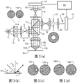
3(a) -3(d) include (a) a schematic of a dark-field scatterometer for measuring a target according to an embodiment of the present invention using a first pair of illuminated apertures, (b) details of the diffraction spectrum of the target grating for a given illumination direction, (c) a second pair of illuminated apertures providing additional illumination modes in using the scatterometer for diffraction-based overlay measurements and (d) a third control perforation that combines the first and second pairs of apertures;
FIG. 4 shows a known form of a multi-grating target and the profile of a measurement spot on a substrate;
FIG. 5 shows an image of the target of FIG. 4 obtained in the scatterometer of FIG. 3;
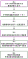
FIG. 6 is a flow chart showing steps of an overlay measurement method using the scatterometer of FIG. 3 and which can be adapted to form an embodiment of the present invention;
FIG. 7 is a flowchart of an extension of step S6 of the flowchart of FIG. 6, according to an embodiment of the invention;
FIG. 8 is a graph of A + and A-for an overlapping grating without feature asymmetry;
FIG. 9 is a diagram of A + and A-for showing an overlapping grating with a characteristic asymmetry of the first embodiment of the present invention;
FIGS. 10a and 10b are diagrams A + and A-for an overlapped grating without a characteristic asymmetry and an overlapped grating with a characteristic asymmetry showing a second embodiment of the present invention;
FIG. 11 is a graph of asymmetry and overlap for an overlapping grating having a characteristic asymmetry;
FIG. 12a is a graph of A + and A-for an overlapping grating with a large degree of feature asymmetry;
FIG. 12b is a diagram of A + -A0 and A-A0 for showing an overlapping grating of a third embodiment of the present invention including a third bias and a large feature asymmetry;
figure 13 shows a composite grating structure with a biasing scheme that may be used in a third embodiment of the invention.
FIG. 14 is a graphical representation of overlay on a wafer and illustrates that correction for process asymmetry minimizes the difference between the overlay estimated at TE and TM radiation;
14(a) and 14(b) show plots of uncorrected overlay measurements on a wafer using TE radiation and TM radiation, respectively;
FIG. 14(c) shows the difference between the measurements of FIGS. 14(a) and 14 (b);
14(d) and 14(e) show diagrams of overlay measurements performed on a wafer using TE radiation and TM radiation, respectively, and having been corrected in accordance with an embodiment of the present invention;
fig. 14(f) shows the difference between the measurements of fig. 14(d) and 14 (e).
The features and advantages of the present invention will be more readily understood from the following detailed description set forth in connection with the accompanying drawings in which like reference characters designate corresponding elements throughout. In the drawings, like reference numbers generally indicate identical, functionally similar, and/or structurally similar elements. The drawing in which an element first appears is indicated by the leftmost digit(s) in the corresponding reference number.
Detailed Description
This specification discloses one or more embodiments that incorporate the features of this invention. The disclosed embodiments are merely exemplary of the invention. The scope of the invention is not limited to the disclosed embodiments. The invention is defined by the appended claims.
The embodiments, as well as "one embodiment," "an embodiment," "example embodiment," etc., referred to in this specification, indicate that the embodiment may include a particular feature, structure, or characteristic, but every embodiment may not necessarily include the particular feature, structure, or characteristic. Moreover, such phrases are not necessarily referring to the same embodiment. Further, when a particular feature, structure, or characteristic is described in connection with an embodiment, it is submitted that it is within the knowledge of one skilled in the art to effect such feature, structure, or characteristic in connection with other embodiments whether or not explicitly described.
Embodiments of the invention may be implemented as hardware, firmware, software, or any combination thereof. Embodiments of the invention may also be implemented as instructions stored on a machine-readable medium, which may be read and executed by one or more processors. A machine-readable medium may include any mechanism for storing or transmitting information in a form readable by a machine (e.g., a computing device). For example, a machine-readable medium may include Read Only Memory (ROM); random Access Memory (RAM); a magnetic disk storage medium; an optical storage medium; a flash memory device; electrical, optical, acoustical or other form of propagated signals, and others. Also, firmware, software, routines, instructions may be described herein as performing certain actions. However, it should be understood that such descriptions are merely for convenience and that such actions in fact result from computing devices, processors, controllers, or other means for executing the firmware, software, routines, instructions, etc.
Before describing embodiments of the present invention in more detail, it makes sense to explain an example environment in which embodiments of the present invention may be practiced.
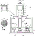
FIG. 1 schematically depicts a lithographic apparatus LA. The apparatus comprises: an illumination system (illuminator) IL configured to condition a radiation beam B (e.g. UV radiation or DUV radiation); a patterning device support or support structure (e.g. a mask table) MT constructed to support a patterning device (e.g. a mask) MA and connected to a first positioner PM configured to accurately position the patterning device in accordance with certain parameters; a substrate table (e.g. a wafer table) WT constructed to hold a substrate (e.g. a resist-coated wafer) W and connected to a second positioner PW configured to accurately position the substrate in accordance with certain parameters; and a projection system (e.g. a refractive projection lens system) PS configured to project a pattern imparted to the radiation beam B by patterning device MA onto a target portion C (e.g. comprising one or more dies) of the substrate W.
The illumination system may include various types of optical components, such as refractive, reflective, magnetic, electromagnetic, electrostatic or other types of optical components, or any combination thereof, for directing, shaping, or controlling radiation.
The patterning device support holds the patterning device in a manner that depends on the orientation of the patterning device, the design of the lithographic apparatus, and other conditions, such as for example whether or not the patterning device is held in a vacuum environment. The patterning device support may use mechanical, vacuum, electrostatic or other clamping techniques to hold the patterning device. The patterning device support may be a frame or a table, for example, which may be fixed or movable as required. The patterning device support may ensure that the patterning device is at a desired position, for example with respect to the projection system. Any use of the terms "reticle" or "mask" herein may be considered synonymous with the more general term "patterning device".
The term "patterning device" used herein should be broadly interpreted as referring to any device that can be used to impart a radiation beam with a pattern in its cross-section such as to create a pattern in a target portion of the substrate. It should be noted that the pattern imparted to the radiation beam may not exactly correspond to the desired pattern in the target portion of the substrate (for example if the pattern includes phase-shifting features or so called assist features). Generally, the pattern imparted to the radiation beam will correspond to a particular functional layer in a device being created in the target portion, such as an integrated circuit.
The patterning device may be transmissive or reflective. Examples of patterning devices include masks, programmable mirror arrays, and programmable LCD panels. Masks are well known in lithography, and include mask types such as binary, alternating phase-shift, attenuated phase-shift, and various hybrid mask types. An example of a programmable mirror array employs a matrix arrangement of small mirrors, each of which can be individually tilted so as to reflect an incoming radiation beam in different directions. The tilted mirrors impart a pattern in a radiation beam which is reflected by the mirror matrix.
The term "projection system" used herein should be broadly interpreted as encompassing any type of projection system, including refractive, reflective, catadioptric, magnetic, electromagnetic and electrostatic optical systems, or any combination thereof, as appropriate for the exposure radiation being used, or for other factors such as the use of an immersion liquid or the use of a vacuum. Any use of the term "projection lens" herein may be considered as synonymous with the more general term "projection system".
As here depicted, the apparatus is of a transmissive type (e.g. employing a transmissive mask). Alternatively, the apparatus may be of a reflective type (e.g. employing a programmable mirror array of a type as referred to above, or employing a reflective mask).
The lithographic apparatus may be of a type having two (dual stage) or more substrate tables (and/or two or more mask tables). In such "multiple stage" machines the additional tables may be used in parallel, or preparatory steps may be carried out on one or more tables while one or more other tables are being used for exposure.
The lithographic apparatus may also be of a type: wherein at least a portion of the substrate may be covered by a liquid having a relatively high refractive index, e.g. water, so as to fill a space between the projection system and the substrate. Immersion liquids may also be applied to other spaces in the lithographic apparatus, for example, between the mask and the projection system. Immersion techniques are well known in the art for increasing the numerical aperture of projection systems. The term "immersion" as used herein does not mean that a structure, such as a substrate, must be submerged in liquid, but rather only means that liquid is located between the projection system and the substrate during exposure.
Referring to FIG. 1, the illuminator IL receives a radiation beam from a radiation source SO. The source and the lithographic apparatus may be separate entities, for example when the source is an excimer laser. In such cases, the source is not considered to form part of the lithographic apparatus and the radiation beam is passed from the source SO to the illuminator IL with the aid of a beam delivery system BD comprising, for example, suitable directing mirrors and/or a beam expander. In other cases the source may be an integral part of the lithographic apparatus (for example when the source is a mercury lamp). The source SO and the illuminator IL, together with the beam delivery system BD if required, may be referred to as a radiation system.
The illuminator IL may comprise an adjuster AD for adjusting the angular intensity distribution of the radiation beam. Generally, at least the outer and/or inner radial extent (commonly referred to as σ -outer and σ -inner, respectively) of the intensity distribution in a pupil plane of the illuminator can be adjusted. IN addition, the illuminator IL may comprise various other components, such as an integrator IN and a condenser CO. The illuminator may be used to condition the radiation beam, to have a desired uniformity and intensity distribution in its cross-section.
The radiation beam B is incident on the patterning device (e.g., mask) MA, which is held on the patterning device support (e.g., mask table MT), and is patterned by the patterning device. Having traversed the patterning device (e.g., mask) MA, the radiation beam B passes through the projection system PS, which focuses the beam onto a target portion C of the substrate W. With the aid of the second positioner PW and position sensor IF (e.g. an interferometric device, linear encoder, two-dimensional encoder or capacitive sensor), the substrate table WT can be moved accurately, e.g. so as to position different target portions C in the path of the radiation beam B. Similarly, the first positioner PM and another position sensor (which is not explicitly depicted in fig. 1) can be used to accurately position the patterning device (e.g. mask) MA with respect to the path of the radiation beam B, e.g. after mechanical retrieval from a mask library, or during a scan. In general, movement of the patterning device support (e.g. mask table) MT may be realized with the aid of a long-stroke module (coarse positioning) and a short-stroke module (fine positioning), which form part of the first positioner PM. Similarly, movement of the substrate table WT may be realized using a long-stroke module and a short-stroke module, which form part of the second positioner PW. In the case of a stepper (as opposed to a scanner) the patterning device support (e.g. mask table) MT may be connected to a short-stroke actuator only, or may be fixed.
Patterning device (e.g. mask) MA and substrate W may be aligned using mask alignment marks M1, M2 and substrate alignment marks P1, P2. Although the substrate alignment marks as shown occupy dedicated target portions, they may be located in spaces between target portions (these are known as scribe-lane alignment marks). Similarly, in situations in which more than one die is provided on the patterning device (e.g. mask) MA, the mask alignment marks may be located between the dies. Small alignment marks may also be included within the die, between device features, in which case it is desirable that the marks be as small as possible and not require any different imaging or processing conditions than adjacent features. An alignment system for detecting alignment marks is described further below.
The illustrated apparatus can be used in at least one of the following modes:
1. in step mode, the patterning device support (e.g. mask table) MT and the substrate table WT are kept essentially stationary, while an entire pattern imparted to the radiation beam is projected onto a target portion C at one time (i.e. a single static exposure). The substrate table WT is then shifted in the X and/or Y direction so that a different target portion C can be exposed. In step mode, the maximum size of the exposure field limits the size of the target portion C imaged in a single static exposure.
2. In scan mode, the patterning device support (e.g. mask table) MT and the substrate table WT are scanned synchronously while a pattern imparted to the radiation beam is projected onto a target portion C (i.e. a single dynamic exposure). The velocity and direction of the substrate table WT relative to the patterning device support (e.g. mask table) MT may be determined by the (de-) magnification and image reversal characteristics of the projection system PS. In scan mode, the maximum size of the exposure field limits the width (in the non-scanning direction) of the target portion in a single dynamic exposure, whereas the length of the scanning movement determines the height (in the scanning direction) of the target portion.
3. In another mode, a patterning device support (e.g. a mask table) MT is kept essentially stationary holding a programmable patterning device, and the substrate table WT is moved or scanned while a pattern imparted to the radiation beam is projected onto a target portion C. In this mode, generally a pulsed radiation source is employed and the programmable patterning device is updated as required after each movement of the substrate table WT or in between successive radiation pulses during a scan. This mode of operation can be readily applied to maskless lithography that utilizes programmable patterning device, such as a programmable mirror array of a type as referred to above.
Combinations and/or variations on the above described modes of use or entirely different modes of use may also be employed.
The lithographic apparatus LA is of the so-called dual stage type having two substrate tables WTa, WTb and two stations, an exposure station and a measurement station, between which the substrate tables may be exchanged. When one substrate on one substrate table is exposed at the exposure station, another substrate may be loaded onto another substrate table at the measurement station and various preparatory steps performed. The preparatory steps may include planning surface control of the substrate using the level sensor LS and measuring the position of alignment marks on the substrate using the alignment sensor AS. This can substantially increase the productivity of the apparatus. IF the position sensor IF is not able to measure the position of the substrate table when the substrate table is in the measurement station and in the exposure station, a second position sensor may be provided to enable the position of the substrate table to be tracked at both stations.
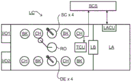
As shown in fig. 2, lithographic apparatus LA forms part of a lithographic cell LC (also sometimes referred to as a lithographic cell or lithographic cluster), which also includes apparatus to perform pre-exposure and post-exposure processing on a substrate. These include a spin coater SC to deposit a resist layer, a developer DE to develop the exposed resist, a chill plate CH, and a bake plate BK. The substrate handler or robot RO picks up the substrates from the input/output ports I/O1, I/O2, then moves them between different processing tools, and then transfers them to the feed table LB of the lithographic apparatus. These devices, often collectively referred to as tracks, are under the control of a track control unit TCU which itself is controlled by a supervisory control system SCS, which also controls the lithographic apparatus via the lithographic control unit LACU. Thus, different equipment may be operated to maximize productivity and processing efficiency.
A micro-diffraction based overlay (μ DBO) metrology device suitable for use in embodiments of the present invention is shown in fig. 3 (a). The target grating T and the diffracted light are shown in more detail in fig. 3 (b). The μ DBO metrology apparatus may be a separate device or comprised in the lithographic apparatus LA (e.g. at a metrology station) or the lithographic cell LC. The optical axis is indicated by the dashed line O, which has a plurality of branches extending through the device. In this apparatus, light emitted by a source 11 (e.g. a xenon lamp) is directed onto a substrate W via a beam splitter 15 by means of an optical system comprising lenses 12, 14 and an objective lens 16. The lenses are arranged in a double sequence of a 4F arrangement. Different lens arrangements may be used as long as such lens arrangements are still capable of providing a substrate image onto the detector and at the same time allow access to intermediate pupil planes for space-frequency filtering. Thus, the range of angles over which radiation is incident on the substrate can be selected by defining in a plane a spatial intensity distribution representing the spatial spectrum of the substrate plane (referred to herein as the (conjugate) pupil plane). This can be done, inter alia, by inserting an aperture plate 13 of suitable form between the lenses 12 and 14 in the plane of the back projection image as the pupil plane of the objective lens. In the example shown, the aperture plate 13 has a different form, marked with 13N and 13S, allowing different illumination modes to be selected. The illumination system in this example forms an off-axis illumination mode. In the first illumination mode, the aperture plate 13N provides off-axis from the direction labeled "N (north)" (for illustrative purposes only). In the second illumination mode, the aperture plate 13S is used to provide similar illumination, but from the opposite direction, labeled "S (south)". Other illumination modes may also be achieved by using different apertures. The rest of the pupil plane is desirably dark, since any unnecessary light outside the desired illumination mode will interfere with the desired measurement signal.
As shown in fig. 3(b), the target grating T and the substrate W are placed orthogonal to the optical axis O of the objective lens 16. The irradiation light I incident on the grating T from an angle deviated from the optical axis O generates a zeroth order light (solid line 0) and two first order lights (one-dot chain line +1 and two-dot chain line-1). It will be appreciated that in the case of an overfilled small target grating, these rays are only one of many parallel rays covering the area of the substrate that includes the metrology target grating T and other features. Since the holes in the plate 13 have a limited width (necessary to allow a useful amount of light to pass through), the incident light rays I will actually occupy an angular range and the diffracted rays 0 and +1/-1 will be diffused. According to the point spread function of a small target, each diffraction order +1 and-1 will be further spread over an angular range, rather than an ideal single ray as shown. Note that the grating pitch and illumination angle can be designed or adjusted so that the first order rays entering the objective lens are closely or closely aligned with the central optical axis. The rays shown in fig. 3(a) and 3(b) are shown off-axis purely to enable them to be more easily distinguished in the figure.
At least the 0 and +1 orders diffracted by the target on the substrate W are collected by the objective lens 16 and directed back through the beam splitter 15. Returning to fig. 3(a), both the first and second illumination modes are shown by designating diametrically opposed apertures labeled north (N) and south (S). When the incident light ray I comes from the north side of the optical axis, i.e., when the first illumination mode is applied using the aperture plate 13N, the +1 diffracted light ray labeled +1(N) enters the objective lens 16. In contrast, when the second illumination mode is applied using the aperture plate 13S, the-1 diffracted light (labeled-1 (S)) is the diffracted light entering the objective lens 16.
The second beam splitter 17 splits the diffracted beam into two measurement branches. In the first measurement branch, the optical system 18 forms a diffraction spectrum (pupil plane image) of the target on a first sensor 19 (e.g., a CCD or CMOS sensor) using the zeroth order and first order diffracted beams. Each diffraction order hits a different point on the sensor so that the image processing can compare and contrast the diffraction orders. The pupil plane image captured by the sensor 19 may be used for a convergence metrology device and/or to normalize the intensity measurements of the first order beam. The pupil plane image may also be used for many measurement purposes, such as reconstruction, which is not the subject of the present disclosure.
In the second measuring branch, the optical system 20, 22 forms an image of the target on the substrate W on a sensor 23 (e.g. a CCD or CMOS sensor). In the second measuring branch, the aperture stop 21 is arranged in a plane conjugate to the pupil plane. The function of the aperture stop 21 is to block the zeroth order diffracted beam so that the image of the target formed on the sensor 23 is formed by only the-1 or +1 first order beams. The images captured by the sensors 19 and 23 are output to an image processor and controller PU, the function of which will depend on the particular type of measurement being made. Note that the term "image" is used herein in a broad sense. If only one of the-1 and +1 diffraction orders is present, an image of the grating lines will not be formed as well.
The particular form of the aperture plate 13 and the field stop 21 shown in fig. 3 is purely exemplary. In another embodiment of the invention, on-axis illumination of the target is used, and an aperture stop with an off-axis aperture is used to pass substantially only one first order diffracted light to the sensor. In other embodiments, second, third, and higher order beams (not shown in FIG. 3) may be used for measurements instead of or in addition to the first order beams.
To enable the illumination to be adapted to these different types of measurements, the aperture plate 13 may include a pattern of apertures formed around a disk that rotates to bring the desired pattern into position. Alternatively or additionally, a set of plates 13 may be provided and exchanged to achieve the same effect. Programmable illumination devices such as deformable mirror arrays or transmissive spatial light modulators may also be used. A moving mirror or prism may be used as another way of adjusting the illumination pattern.
As explained just with regard to the aperture plate 13, the selection of the diffraction orders used for imaging can alternatively be achieved by modifying the pupil stop (pupil-stop)21 or by replacing a pupil stop with a different pattern or by replacing a fixed field stop with a programmable spatial light modulator. In this case, the irradiation side of the measurement optical system can be kept constant while the imaging side has the first and second modes. Thus, in the present disclosure, there are effectively three types of measurement methods, each with its own advantages and disadvantages. In one approach, the illumination mode is changed to measure different diffraction orders. In another approach, the imaging mode is changed. In a third method, the illumination mode and the imaging mode remain unchanged, but the target is rotated 180 degrees. In each case, the desired effect is the same, i.e. a first and a second part of the non-zero order diffracted radiation are selected, which are symmetrically opposite to each other in the diffraction spectrum of the target. In principle, the desired selection of the diffraction order may be obtained by simultaneously changing the combination of illumination mode and imaging mode, but this may bring disadvantages without advantages, and therefore it will not be discussed further.
Although the optical system used for imaging in this example has a wide entrance pupil bounded by field stop 21, in other embodiments or applications, the entrance pupil size of the imaging system itself may be small enough to be bounded to the desired diffraction orders, and therefore also serve as a field stop. Different orifice plates are shown in fig. 3(c) and 3(d), which may be used, as described further below.
Typically, the target grating will be aligned with its grating lines extending either north-south or east-west. That is, the grating will be aligned in the X-direction or Y-direction of the substrate W. Note that the aperture plate 13N or 13S may be used to measure gratings that are oriented in one direction only (X or Y, depending on the setting). For the measurement of orthogonal gratings, target rotation through 90 and 270 degrees can be achieved. More conveniently, however, illumination from east or west is provided in the illumination optics using an aperture plate 13E or 13W, as shown in fig. 3 (c). The orifice plates 13N to 13W may be formed and interchanged independently, or they may be a single orifice plate capable of rotating 90, 180, or 270 degrees. As already described, the off-axis aperture as shown in fig. 3(c) may be provided in the field stop 21 instead of the illumination aperture plate 13. In this case, the irradiation will be along the axis.
FIG. 3(d) shows a third pair of aperture plates that may be used to combine the illumination patterns of the first and second pairs of aperture plates. The orifice plate 13NW has orifices located north and east, and the orifice plate 13SE has orifices located south and west. Given that the cross-talk between these different diffraction signals is not too great, the measurement of both the X-grating and the Y-grating can be made without changing the illumination mode.
Figure 4 illustrates a composite target formed on a substrate according to known practice. The composite target comprises four gratings 32 to 35 positioned closely together so that they will all be within the measurement spot 31 formed by the illumination beam of the metrology apparatus. Thus, four targets are all simultaneously illuminated and simultaneously imaged on the sensors 19 and 23. In one example dedicated to overlay measurement, the gratings 32 to 35 are themselves composite gratings formed by overlay gratings that are patterned in different layers of a semiconductor device formed on the substrate W. The gratings 32 to 35 may have overlap offsets that are biased differently to facilitate overlap measurements between layers in which different portions of the composite grating are formed. The gratings 32 to 35 may also have different orientations, as shown, in order to diffract incident radiation in the X and Y directions. In one example, gratings 32 and 34 are X-direction gratings with + d, -d biases, respectively. This means that the gratings 32 have their overlapping components or compositions arranged such that if they were all printed exactly at their nominal position, one of them would be offset from the other by a distance d. The grating 34 has its components or composition arranged such that there will be a bias of d if printed intact, but in the opposite direction to that of the first grating, and so on. The gratings 33 and 35 are Y-direction gratings with offsets + d and-d, respectively. Although four gratings are shown, another embodiment may require a larger matrix to achieve the desired accuracy. For example, a 3 × 3 array of 9 composite gratings may have offsets of-4 d, -3d, -2d, -d, 0, + d, +2d, +3d, +4 d. The individual images of these gratings may be identified in the image captured by the sensor 23.
Fig. 5 shows an example of an image that may be formed on the sensor 23 using the aperture plate 13NW or 13SE as shown in fig. 3(d) and detected by the sensor 23 using the target of fig. 4 in the apparatus of fig. 3. Although the pupil plane image sensor 19 cannot resolve the different individual gratings 32 to 35, the image sensor 23 can resolve the different individual gratings 32 to 35. The dark rectangle represents the image field on the sensor, where the illumination spot 31 on the substrate is imaged into the corresponding circular area 41. In this region, rectangular areas 42-45 represent the images of the small target gratings 32 to 35. If the grating is located in the product area, product features may also be visible at the periphery of the image field. The image processor and controller PU processes these images using pattern recognition to identify the individual images 42 to 45 of the rasters 32 to 35. In this way, the images do not have to be aligned very precisely at specific positions within the sensor frame, which greatly increases the productivity of the measuring device as a whole. However, if the imaging process is affected by non-uniformities in the image field, the requirement for precise alignment remains. In one embodiment of the invention, four positions P1-P4 are identified and the gratings are aligned as much as possible with these known positions.
Once the individual images of the raster have been identified, the intensity of those individual images can be measured, for example by averaging or summing selected pixel intensity values in the identified region. The intensity and/or other properties of the images may be compared to each other. These results may be combined to measure different parameters of the lithographic process. Overlay performance is an important example of such a parameter, and is also a measure of the lateral alignment of the two lithographic layers. The overlap may be defined more specifically, for example, as a lateral position difference between a center of a top of a bottom grating and a center of a bottom of a corresponding top grating.
Examples of dark field measurements may be found in international patent applications WO2009/078708 and WO2009/106279, both of which are incorporated herein by reference in their entirety. Further developments of this technology have been described in patent publications US20110027704A, US20110043791A and US 20120123581. The contents of all of these applications are also incorporated herein by reference.
Fig. 6 shows how the overlay error between two layers containing component gratings or component gratings 32 to 35 can be measured, for example using the method described in application WO2011/012624, by the asymmetry of the gratings, which is obtained by comparing their intensities in the +1 and-1 order dark field images. In step S1, a substrate, such as a semiconductor wafer, is processed one or more times by the lithography unit of fig. 2 to form a structure including the overlay targets 32-35. In step S2, using the metrology apparatus of FIG. 3, an image of the gratings 32-35 is obtained using only one of the first order diffracted beams (e.g., -1 order diffracted beam). Then, by changing the illumination mode, or changing the imaging mode, or by rotating the substrate W180 degrees in the field of view of the metrology apparatus, a second image of the grating may be obtained with another first order diffracted beam (+1) (step S3). Thus, +1 st order diffracted radiation is captured in the second image.
Note that by including only half of the first order diffracted radiation in each image, the "image" described herein is not a conventional dark-field microscope image. The individual grating lines will not be resolved. Each grating is represented only by an area having a certain intensity level. In step S4, a region of interest (ROI) is carefully identified within the image of each component grating or component grating (constituent grating), from which the intensity level is to be measured. This is done because, especially near the edges of the individual grating images, in general, the intensity values may be highly dependent on process variables such as resist thickness, composition, line shape, and edge effects.
The ROI has been identified and its intensity measured for each individual grating, so that the asymmetry of the grating structure, and hence the overlay error, can be determined. This is done by: the intensity values obtained by the image processor and controller PU for the +1 and-1 diffraction orders of each grating 32-35 are compared in step S5 to identify any differences in their intensities, and (S6) an overlay error near the target T is determined from knowledge of the overlay bias of the gratings.
In the above-described prior applications, various techniques for improving the quality of overlay measurement using the above-described basic method are disclosed. For example, the intensity difference between images can be attributed to differences in the optical paths for different measurements, rather than being purely asymmetry in the target. The illumination source 11 may be such that the intensity and/or phase of the illumination spot 31 is non-uniform. A correction may be determined and applied to minimize such errors with reference to, for example, the position of the target image in the image field of the sensor 23. These techniques are explained in the prior art applications and the details will not be explained further here. They can be used in combination with the newly disclosed techniques in the present application, which will be described below.
Overlay measurement according to this method assumes that the measured asymmetry is only proportional to the actual overlay shift between grating layers. This is not necessarily the case, however, since the measured asymmetry is also affected by the effect of the feature asymmetry that occurs in the fabrication of the grating. These characteristic asymmetry effects include side wall angle asymmetry and bottom tilt (floor-tilt), and disturb overlay measurements based on first order asymmetry. This will result in an offset in the measurement results and hence in an inaccurate overlay measurement.
FIG. 7 is a flowchart adapted to step S6 in the flowchart of FIG. 6 to analyze diffraction-based overlay measurements (DBO and μ DBO) using A + to A-regression by determining positively-biased grating A + as a function of the asymmetry of negatively-biased grating A-. In step S6-1, A + and A-are determined for different numbers of measured pupil pixels and/or different numbers of wavelength polarization combinations (i.e., numbers for different illumination conditions or illumination "recipes"). Thereafter, in step S6-2, the determined value of A + is plotted against the determined value of A-to derive the overlap.
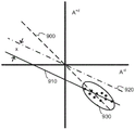
FIG. 8 is a graph for A + versus A-for an overlapped grating without a characteristic asymmetry that enables the only asymmetry that exists to be that due to bias and overlap. In this case, the relationship between A + and A-is on a straight line passing through the origin. It is clear that all the measured wavelength-polarization combinations are on this line. The slope of the line is related to the overlap. Four lines are shown in the figure:
the dashed line labeled OV ═ 0 is the line representing zero overlap, with a slope of-1;
the dashed line labeled OV → ∞ is a line having a slope of +1, indicating that the overlap tends to infinity;
the solid line labeled OV <0 is a line with a slope less than-1, which indicates that the overlap is less than 0; and
the solid line labeled OV >0 is a line with a slope greater than-1, which indicates an overlap greater than 0.
In addition, it can be seen that an overlap equal to + d will result in the drawn line being along the y-axis, while an overlap equal to-d will result in the drawn line being along the x-axis, where d is the grating bias.
It is proposed to use a + versus a-regression to:
measuring the overlap that would be correct in the absence of the asymmetry attributable to the feature by determining the slope of a line fitted through the data set, the line not necessarily fitting through the origin;
analysis of the feature asymmetry on the wafer can be done via the offset of the line from the origin (i.e. from the intercept term);
optimization of the illumination matching scheme is performed by selecting the wavelength-polarization combination that is least sensitive to the characteristic asymmetry.
FIG. 9 is a diagram of A + versus A-showing the first two of these aspects, such as may be depicted in step S6-2. The data points 930 will be fitted to a line 900 passing through the origin according to known methods discussed above. However, in this embodiment, the data points are fitted by a line 910 according to a best fit method (e.g., least squares), the line 910 not necessarily passing through the origin (step S6-3). Thus, the overlap may still be calculated from the slope of the line 910 (step S6-4); it can be seen that line 910 is parallel to line 920 which represents a line that can be seen from the same measured structure that does not have a characteristic degree of asymmetry. The axis intercept of line 910, i.e., the offset of line 910 from line 920 (a line having the same slope as line 910 but not passing through the origin) represents the effect of the feature asymmetry in a normalized manner (step S6-5).
With the overlay bias d of the two symmetrically biased gratings of the target and the slope (slope) of line 910, the overlay can be calculated from fig. 9 (with the aid of the linearized relationship between asymmetry and overlay):

for a pitch periodic sinusoidal relationship, overlap can be similarly understood as:

where pitch is the grating pitch.
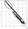
Figure 10a is a graph of a + vs. a-for a grating without a characteristic asymmetry, for (simulated) data for different polarization-wavelength combinations. It can be seen that all data fit on the same line as previously discussed. Fig. 10b shows a similar graph to fig. 10a but with a characteristic asymmetry (especially 0.5nm bottom tilt). In both cases, the data marked by circles represent TE radiation and the data marked by crosshairs represent TM radiation. Although not seen here, the position along the line is determined to a large extent by the wavelength (for a given polarisation) so that shorter (violet) wavelengths tend to be found at the upper end of the line (a + ═ 6 to 8) and longer (red) wavelengths tend to be found at the lower end of the line.
As can be seen from fig. 10b, the wavelength and polarization dependent deviations from the linear relationship are observed in the region 1000 around the origin. In this example of a bottom tilt of 0.5nm, the overlap sensitivity is minimal for the TE polarization. Moreover, the data with the largest value of K (the scaling factor between overlap and asymmetry), i.e. the largest sensitivity to overlap, can also be easily identified, which is the data 1010 which still shows the linear relationship furthest from the origin. In this example, the data 1010 is for radiation in the short wavelength (violet) region. Thus, the illustration, for example, allows for the selection of an optimized illumination recipe (optional step S6-6) that, when used to measure gratings, generates data 1010 that is most sensitive to overlay and least dependent on feature asymmetry.
In actual overlay recipe optimization, multiple measurements on the wafer should be made for different colors and polarizations, so that all possible feature asymmetries on the wafer (e.g., at the edges) are considered. Once the optimal matching scheme is selected, it can be performed by means of this single wavelength-polarization-aperture combination.
If none of the single wavelength-polarization-hole combinations are providing sufficient robustness to feature asymmetry, then the method combined with the A + versus A-regression analysis described above can be used to identify combinations of 2 or 3 settings. This is the case where each individual setting produces a cloud of data entries and the non-zero axis truncation is shown by a line of 2 to 3 settings, the slope of such a line will still produce reasonably asymmetric robust overlapping data. For this reason, 2 or 3 settings are required for this actual overlay measurement.
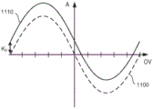
Fig. 11 shows that the characteristic asymmetry results in a vertical offset K0 in the data plotted in the graph of asymmetry a versus overlap OV. Line 1100 fits data for grating structures that do not have asymmetry, while line 1110 fits data for grating structures that have some asymmetry. A ═ K1 sin (ov) may be shown.
For very large feature asymmetries, the methods disclosed herein show significant deviation from a line. This is shown in figure 12a, which shows simulated data on an a + vs a-plot for a grating with a large degree of characteristic asymmetry (note: in this model, K0 is constant across the pupil). It can be seen that the data points do not all lie on or near a line, which makes fitting these data very difficult.
To counteract such a problem, a third grating (or grating pair) may be used in addition to the above-described method, such that the grating structure comprises gratings with three different biases. In a specific embodiment, in addition to the + d and-d gratings, a grating without any bias is provided. This enables the extraction of a relative asymmetry, which can be depicted in the graph of A + -A0 versus A-A0 (FIG. 12 b), where A0 is the asymmetry of the zero-biased grating. It can be seen that the resulting data is less sensitive to feature asymmetry (all data points are substantially on the same line), which enables overlap to be extracted even in the presence of large feature asymmetries. It should be noted that in this embodiment, K0 is allowed to vary across the pupil. Such measurements can be used to determine whether there is a feature asymmetry in the stack. Using this method, the asymmetry a can be calculated as:
A=K0+K1 sin(OV)
this results in the following error reduction compared to the two offset example:

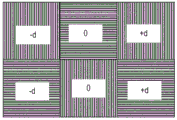
a suitable grating structure for use in this method is shown in figure 13. It includes two orthogonal gratings with a negative bias-d, two orthogonal gratings with a zero bias, and two orthogonal gratings with a positive bias + d. Such a grating structure can be directly applied to small target designs, as for μ DBO targets.
This method may be combined with other methods described herein. For example, process asymmetry sensitivity can be reduced by fitting scheme optimization, experimentally by choosing the least sensitive wavelength and polarization.
In summary, an overlap analysis and fitting scheme selection method using regression of a first bias asymmetry to a second bias asymmetry may include:
minimum 'pupil- σ' analysis (fitting the best fitting solution on the line, e.g. in least squares);
process handling-analysis of asymmetry sensitivity (offset of the line from the origin or no linear dependence therein);
model consistency tests on the pupils of the 'linear' and 'ATAN' models; and
analysis of process asymmetry on a wafer.
Further, it should be noted that the proposed selection of the recipe and the overlap analysis method do not require any overlay information to perform.
For pupil-based analysis, the method disclosed herein correctly includes data points at which the K value (the scaling factor between the overlap and the asymmetry) changes sign. This potentially extends the range of available recipe settings for good measurements and enables selection based on other parameters such as linear range, for example.
It has been disclosed above that the overlap can be estimated from the slope of the regressed line 910, for example as shown in fig. 9. The feature asymmetry in the stack shifts the line of regression away from the origin. This shift in the regression line effectively discriminates the feature asymmetry.
It is also proposed to correct the estimated overlay on the wafer by using this shift in the measured asymmetry. If a wafer measurement is given, the covariance between the estimated overlay and the measured offset of asymmetry clearly shows that there is a correlation between the two measurements on the wafer. It is then proposed to correct the estimated overlap on the wafer according to the measured offset of the asymmetry. In order to find the optimal correction, a minimization means (e.g. linear minimization, such as least squares) can be established which minimizes the difference between the overlap estimated by means of TE polarized radiation and the overlap estimated by means of TM polarized radiation.
Such a method may comprise the steps of:
method steps S6-1 through S6-5 are performed at multiple locations on the wafer (respectively) using both TE polarized radiation and TM polarized radiation. Due to these measurements, estimates of the overlay (line slope) and process asymmetry (line offset) at each wafer position will be obtained for both the TE polarized radiation and the TM polarized radiation.
The difference between the overlap estimated by means of TE-polarized radiation and the overlap estimated by means of TM-polarized radiation, estimated in the previous step, is minimized in order to find a correction for the estimated overlap on the wafer according to the measured process asymmetry.
Fig. 14 shows that correcting for the process asymmetry minimizes the difference between the overlaps estimated by means of TE and TM radiation. Fig. 14(a) and 14(b) show graphs of uncorrected overlay measurements on a wafer using TE radiation and TM radiation, respectively. Fig. 14(c) is the difference between the measurements of fig. 14(a) and 14 (b). Fig. 14(d) and 14(e) show diagrams of overlay measurements on a wafer using TE radiation and TM radiation, respectively, which have been modified according to this embodiment. Fig. 14(f) is the difference between the measurements of fig. 14(d) and 14 (e). It can clearly be seen that the difference between the TE and TM overlay measurements for the corrected overlay measurement is smaller than the difference between the TE and TM overlay measurements for the uncorrected overlay measurement.
With further evidence of the role of this method, the overlay was independently calculated on 3 independent data sets corresponding to 3 independent wavelength TE/TM measurement pairs. The difference in estimated overlap between these 3 data sets is taken into account. It can be seen that the Root Mean Square (RMS) of the difference in overlap measured by means of independent wavelength and polarization is improved by 0.2nm for both the x and y directions, which results in an accuracy improvement of 70%.
Additionally, it is noted that the techniques disclosed herein may be applied to large scatterometer targets (also referred to as standard targets). With the apparatus of fig. 3, for example, the overlap in these larger objects can be measured by an angle-resolved scatterometer using the pupil image sensor 19 instead of or in addition to the measurements made in the dark-field imaging branch and sensor 23.
The goal in this scheme also allows standard overlay calculation methods ('linear' and 'ATAN' methods) to be applied based on this measurement, without taking into account bottom-grating asymmetry (BGA).
Although the target structures described above are metrology targets specifically designated and formed for measurement purposes, in other embodiments, the properties may be measured on targets that are functional portions of devices formed on the substrate. Many devices have a regular grating-like structure. The terms 'target grating' and 'target structure' as used herein do not require that the structure is already specifically provided for the measurement being taken.
In connection with a physical grating structure of a target implemented on a substrate and a patterning device, an embodiment may include a computer program containing one or more sequences of machine-readable instructions describing a method of measuring a target on a substrate and/or analysing the measurements to obtain information about a lithographic process. The computer program may be executed, for example, in the unit PU in the device of fig. 3 and/or in the control unit LACU of fig. 2. A data storage medium (e.g. a semiconductor memory, a magnetic or optical disk) may also be provided, having the computer program stored therein. In the case where an existing metrology apparatus (e.g., of the type shown in FIG. 3) is already in production and/or use, the present invention may be implemented by providing an updated computer program product for causing a processor to perform modified step S6 (including steps S6-1 through S6-6) and thereby calculate overlay errors with reduced sensitivity to feature asymmetry. The program may optionally be arranged to control an optical system, substrate support or similar component to perform steps S2-S5 for measurement of asymmetry on a suitable plurality of target structures.
Although specific reference may have been made above to the use of embodiments of the invention in the context of optical lithography, it will be appreciated that the invention may be used in other applications, for example imprint lithography, and where the context allows, is not limited to optical lithography. In imprint lithography, a topography in a patterning device defines the pattern created on a substrate. The topography of the patterning device can be printed into a layer of resist supplied to the substrate whereupon the resist is cured by applying electromagnetic radiation, heat, pressure or a combination thereof. After the resist is cured, the patterning device is removed from the resist, leaving a pattern in the resist.
The terms "radiation" and "beam" used herein encompass all types of electromagnetic radiation, including: ultraviolet radiation (UV), e.g. having a wavelength of or about 365, 355, 248, 193, 157 or 126nm, and extreme ultra-violet (EUV) radiation, e.g. having a wavelength in the range of 5-20nm, as well as particle beams, such as ion beams or electron beams.
The term "lens", where the context allows, may refer to any one or combination of various types of optical components, including refractive, reflective, magnetic, electromagnetic and electrostatic optical components.
The foregoing description of the specific embodiments will so fully reveal the general nature of the invention that others can, by applying knowledge within the skill of the art, readily modify and/or adapt for various applications such specific embodiments without undue experimentation and without departing from the general concept of the present invention. Therefore, such modifications and adaptations are intended to be within the scope and meaning of equivalents of the disclosed embodiments, based on the teaching and teachings herein. It is to be understood that the phraseology or terminology herein is for the purpose of description and not of limitation, such that the terminology or phraseology of the present specification is to be interpreted by the skilled artisan in light of the teachings and guidance.
The breadth and scope of the present invention should not be limited by any of the above-described exemplary embodiments, but should be defined only in accordance with the following claims appended hereto and their equivalents.
It should be appreciated that the detailed description section, and not the summary and abstract sections, is intended to be used to interpret the claims. The summary and abstract sections may set forth one or more, but not all exemplary embodiments of the present invention as contemplated by the inventors, and are therefore not intended to limit the present invention and the appended claims in any way.
The invention has been described above with the aid of functional building blocks illustrating embodiments of specific functions and relationships thereof. For convenience of description, the boundaries of these functional building blocks have been arbitrarily defined herein. Alternate boundaries can be defined so long as the specified functions and relationships thereof are appropriately performed.
The foregoing description of the specific embodiments will so fully reveal the general nature of the invention that others can, by applying knowledge within the skill of the art, readily modify and/or adapt for various applications such specific embodiments without undue experimentation and without departing from the general concept of the present invention. Therefore, such modifications and adaptations are intended to be within the scope and meaning of equivalents of the disclosed embodiments, based on the teaching and teachings herein. It is to be understood that the phraseology or terminology herein is for the purpose of description and not of limitation, such that the terminology or phraseology of the present specification is to be interpreted by the skilled artisan in light of the teachings and guidance.
The breadth and scope of the present invention should not be limited by any of the above-described exemplary embodiments, but should be defined only in accordance with the following claims appended hereto and their equivalents.
Claims (25)
1. A method of measuring a parameter of a lithographic process, the method comprising:
(a) illuminating target structures on a substrate and detecting radiation scattered by each target structure to obtain an asymmetry measurement for each target structure indicative of an overall asymmetry, the target structures comprising at least a first target structure comprising overlapping periodic structures with a first intentional overlay bias and a second target structure comprising overlapping periodic structures with a second intentional overlay bias, the overall asymmetry comprising contributions due to (i) intentional overlay bias in the target structures, (ii) overlay errors in a lithographic process during formation of the target structures, and (iii) feature asymmetries in one or more of the periodic structures;
(b) repeating step (a) for a plurality of different illumination conditions to obtain asymmetry measurement data;
(c) performing a regression analysis on the asymmetry measurement data by fitting a linear regression model to a planar representation of the asymmetry measurement for the first target structure versus the asymmetry measurement for the second target structure, the linear regression model being fitted or not fitted to an origin represented by the plane; and
(d) determining an overlay error from the gradient described by the linear regression model;
wherein the method further comprises:
determining the contribution to the overall asymmetry due to the feature asymmetry according to an intercept term of the linear regression model;
determining an overlay correction that is a function of the determined contribution to the overall asymmetry due to the feature asymmetry; and
the overlay error is corrected using the overlay correction.
2. The method of claim 1, comprising:
performing steps (a) to (d) to determine overlay error measurements for a plurality of different locations on the substrate such that the overlay error measurements for each location are obtained using TE polarized radiation and using TM polarized radiation; and
the overlay correction is calculated by minimizing the difference between the overlay error measured when measuring with TE polarized radiation and the overlay error measured when measuring with TM polarized radiation.
3. The method of claim 1, wherein the linear regression model fitted to asymmetry measurements is fitted only to asymmetry measurement data that is in a region of origin.
4. The method of claim 3, comprising: one or more optimized illumination conditions for which the characteristic asymmetry contributes least to the measured overall asymmetry are identified from a plurality of illumination conditions, the optimized illumination conditions being selected from illumination conditions for which the measured asymmetry lies on or near a shift line, the shift line being a shift line described by the linear regression model but having an intercept term of zero such that it lies on the origin.
5. The method of claim 4, wherein the optimized illumination condition is selected from illumination conditions for which the measured asymmetry is farthest from any measured asymmetry that is not located on or near a bias line.
6. The method of claim 4, comprising: subsequent measurements of structures on the substrate are made using one or more of the optimized illumination conditions.
7. A method according to any of claims 1-6 wherein the first intentional overlay bias is a positive overlay bias and the second intentional overlay bias is a negative overlay bias.
8. A method as claimed in claim 7, wherein the first deliberate overlay bias and the second deliberate overlay bias are of equal magnitude.
9. The method of any one of claims 1-6, wherein step (d) is performed based on the following assumption: the contribution due to feature asymmetry is constant for all overlap values.
10. The method according to any of claims 1-6, wherein the target structure comprises a third target structure without an intentional overlay bias, and the method comprises: determining a relative asymmetry measurement from a difference between the asymmetry measurements obtained in step (b) for the first and third target structures and from a difference between the asymmetry measurements obtained in step (b) for the second and third target structures.
11. The method of claim 10, wherein step (c) comprises: a linear regression model is fitted to a planar representation of the difference of the asymmetry measurement for the first target structure and the asymmetry measurement for the third target structure versus the difference of the asymmetry measurement for the second target structure and the asymmetry measurement for the third target structure.
12. The method of claim 10, wherein step (d) is performed without the following assumptions: the contribution due to feature asymmetry is constant for all overlap values.
13. A method according to any of claims 1-6, comprising an initial step of forming a target structure on a substrate using a lithographic process.
14. An inspection apparatus for measuring a parameter of a lithographic process, the inspection apparatus comprising:
a support for a substrate having a plurality of target structures thereon, the target structures including at least a first target structure and a second target structure, the first target structure including an overlapping periodic structure having a first intentional overlay bias, the second target structure including an overlapping periodic structure having a second intentional overlay bias;
an optical system operable to illuminate the targets and to detect radiation scattered by each target to obtain, for each target structure and for a plurality of different illumination conditions, an asymmetry measurement representing an overall asymmetry comprising contributions due to (i) intentional overlay bias in the target structure, (ii) overlay error in a lithographic process during formation of the target structure, and (iii) feature asymmetry in one or more of the periodic structures;
a processor arranged to:
performing a regression analysis on the asymmetry measurement data by fitting a linear regression model to a planar representation of the asymmetry measurement for the first target structure versus the asymmetry measurement for the second target structure, the linear regression model being fitted or not fitted through an origin of the planar representation, the processor being operable to determine a contribution to the overall asymmetry due to the feature asymmetry from an intercept term of the linear regression model; and
determining an overlay error from the gradient described by the linear regression model; wherein the inspection apparatus is operable to:
determining an overlay correction that is a function of the determined contribution to the overall asymmetry due to the feature asymmetry; and
the overlay error is corrected using the overlay correction.
15. The inspection apparatus of claim 14, operable to:
performing steps (a) to (d) to determine overlay error measurements for a plurality of different locations on the substrate such that the overlay error measurements for each location are obtained using TE polarized radiation and using TM polarized radiation; and
the overlay correction is calculated by minimizing the difference between the overlay error measured when measuring with TE polarized radiation and the overlay error measured when measuring with TM polarized radiation.
16. An inspection apparatus according to claim 14, wherein the processor is operable to fit the linear regression model only to asymmetry measurement data in the region of the origin.
17. The inspection apparatus of claim 16, wherein the processor is operable to identify one or more optimized illumination conditions for which a characteristic asymmetry contributes least to the measured overall asymmetry, from a plurality of illumination conditions, the optimized illumination conditions being selected from illumination conditions for which the measured asymmetry lies on or near a shift line, the shift line being a shift line described by a linear regression model but with an intercept term of zero such that it lies on an origin.
18. The inspection apparatus of claim 17, wherein the processor is operable to select the optimized illumination condition from the illumination conditions for which the measured asymmetry is furthest from any measured asymmetry that is not located on or near a bias line.
19. An inspection apparatus according to claim 17, operable to perform subsequent measurements of structures on a substrate using one or more of the optimised illumination conditions.
20. An inspection apparatus according to any one of claims 14 to 19, wherein the first deliberate overlay bias is a positive overlay bias and the second deliberate overlay bias is a negative overlay bias.
21. An inspection apparatus according to claim 20, wherein the first deliberate overlay bias and the second deliberate overlay bias are of equal magnitude.
22. The inspection apparatus of any of claims 14 to 19, wherein the processor is operable to determine an overlay error from a gradient described by the linear regression model based on the following assumptions: the contribution due to feature asymmetry is constant for all overlap values.
23. An inspection apparatus according to any of claims 14 to 19, wherein the target structures include a third target structure having no intentional overlay bias, and the processor is operable to determine a relative asymmetry measurement from a difference between asymmetry measurements for the first and third target structures and from a difference between asymmetry measurements for the second and third target structures.
24. The inspection apparatus of claim 23, wherein the processor is operable to fit a linear regression model to a planar representation of a difference of the asymmetry measurement for the first target structure and the asymmetry measurement for the third target structure versus a difference of the asymmetry measurement for the second target structure and the asymmetry measurement for the third target structure.
25. The inspection apparatus of claim 23, wherein the processor is operable to determine an overlay error from a gradient described by the linear regression model without the assumption that: the contribution due to feature asymmetry is constant for all overlap values.
Applications Claiming Priority (5)
| Application Number | Priority Date | Filing Date | Title |
|---|---|---|---|
| US201361863150P | 2013-08-07 | 2013-08-07 | |
| US61/863,150 | 2013-08-07 | ||
| US201461975312P | 2014-04-04 | 2014-04-04 | |
| US61/975,312 | 2014-04-04 | ||
| CN201480044257.5A CN105452962B (en) | 2013-08-07 | 2014-07-18 | Method for measurement and equipment, etching system and device making method |
Related Parent Applications (1)
| Application Number | Title | Priority Date | Filing Date |
|---|---|---|---|
| CN201480044257.5A Division CN105452962B (en) | 2013-08-07 | 2014-07-18 | Method for measurement and equipment, etching system and device making method |
Publications (2)
| Publication Number | Publication Date |
|---|---|
| CN108398856A CN108398856A (en) | 2018-08-14 |
| CN108398856B true CN108398856B (en) | 2020-10-16 |
Family
ID=51211228
Family Applications (2)
| Application Number | Title | Priority Date | Filing Date |
|---|---|---|---|
| CN201810061591.1A Active CN108398856B (en) | 2013-08-07 | 2014-07-18 | Metrology method and apparatus, lithographic system and device manufacturing method |
| CN201480044257.5A Active CN105452962B (en) | 2013-08-07 | 2014-07-18 | Method for measurement and equipment, etching system and device making method |
Family Applications After (1)
| Application Number | Title | Priority Date | Filing Date |
|---|---|---|---|
| CN201480044257.5A Active CN105452962B (en) | 2013-08-07 | 2014-07-18 | Method for measurement and equipment, etching system and device making method |
Country Status (8)
| Country | Link |
|---|---|
| US (4) | US9910366B2 (en) |
| JP (2) | JP6336068B2 (en) |
| KR (2) | KR102124204B1 (en) |
| CN (2) | CN108398856B (en) |
| IL (1) | IL243854B (en) |
| NL (1) | NL2013210A (en) |
| TW (3) | TWI636341B (en) |
| WO (1) | WO2015018625A1 (en) |
Families Citing this family (78)
| Publication number | Priority date | Publication date | Assignee | Title |
|---|---|---|---|---|
| US9927718B2 (en) * | 2010-08-03 | 2018-03-27 | Kla-Tencor Corporation | Multi-layer overlay metrology target and complimentary overlay metrology measurement systems |
| US10890436B2 (en) | 2011-07-19 | 2021-01-12 | Kla Corporation | Overlay targets with orthogonal underlayer dummyfill |
| NL2011477A (en) * | 2012-10-10 | 2014-04-14 | Asml Netherlands Bv | Mark position measuring apparatus and method, lithographic apparatus and device manufacturing method. |
| WO2014062972A1 (en) * | 2012-10-18 | 2014-04-24 | Kla-Tencor Corporation | Symmetric target design in scatterometry overlay metrology |
| NL2013210A (en) | 2013-08-07 | 2015-02-10 | Asml Netherlands Bv | Metrology method and apparatus, lithographic system and device manufacturing method. |
| SG11201703585RA (en) * | 2014-11-25 | 2017-06-29 | Kla Tencor Corp | Analyzing and utilizing landscapes |
| EP3224676A1 (en) | 2014-11-26 | 2017-10-04 | ASML Netherlands B.V. | Metrology method, computer product and system |
| CN107430350B (en) | 2015-02-04 | 2019-10-18 | Asml荷兰有限公司 | Metering method and equipment, computer program and lithography system |
| CN107533299B (en) * | 2015-04-10 | 2021-04-02 | Asml荷兰有限公司 | Method and apparatus for detection and measurement |
| JP6524256B2 (en) * | 2015-04-21 | 2019-06-05 | エーエスエムエル ネザーランズ ビー.ブイ. | Metrology method and apparatus, computer program, and lithography system |
| TWI656409B (en) * | 2015-09-09 | 2019-04-11 | 美商克萊譚克公司 | A new method based on the introduction of auxiliary electromagnetic field to superimpose first-order scattering measurement |
| KR102351636B1 (en) * | 2015-09-21 | 2022-01-13 | 케이엘에이 코포레이션 | Process control method and system using flexible sampling |
| CN108431695B (en) | 2015-12-24 | 2020-07-21 | Asml荷兰有限公司 | Method of controlling a patterning process, device manufacturing method, control system for a lithographic apparatus and lithographic apparatus |
| JP6644898B2 (en) | 2016-02-19 | 2020-02-12 | エーエスエムエル ネザーランズ ビー.ブイ. | Method for measuring structure, inspection apparatus, lithography system, device manufacturing method, and wavelength selective filter used therein |
| KR102188711B1 (en) | 2016-02-26 | 2020-12-09 | 에이에스엠엘 네델란즈 비.브이. | Method for measuring structure, inspection apparatus, lithographic system and device manufacturing method |
| US20170256465A1 (en) | 2016-03-01 | 2017-09-07 | Asml Netherlands B.V. | Method and apparatus to determine a patterning process parameter |
| CN111736436B (en) | 2016-04-22 | 2023-08-18 | Asml荷兰有限公司 | Determination of stack differences and correction using stack differences |
| US10115621B2 (en) | 2016-05-13 | 2018-10-30 | Globalfoundries Inc. | Method for in-die overlay control using FEOL dummy fill layer |
| US10481504B2 (en) * | 2016-06-10 | 2019-11-19 | Imec Vzw | Method and apparatus for semiconductor manufacturing |
| IL263765B2 (en) | 2016-07-15 | 2023-04-01 | Asml Netherlands Bv | Method and apparatus for design of a metrology target field |
| US10048132B2 (en) * | 2016-07-28 | 2018-08-14 | Kla-Tencor Corporation | Simultaneous capturing of overlay signals from multiple targets |
| EP3293574A1 (en) | 2016-09-09 | 2018-03-14 | ASML Netherlands B.V. | Metrology method, apparatus and computer program |
| EP3299890A1 (en) | 2016-09-27 | 2018-03-28 | ASML Netherlands B.V. | Metrology recipe selection |
| WO2018059824A1 (en) | 2016-09-27 | 2018-04-05 | Asml Netherlands B.V. | Metrology recipe selection |
| CN110140087B (en) * | 2016-11-10 | 2021-08-13 | Asml荷兰有限公司 | Design and correction using stack differences |
| EP3333631A1 (en) | 2016-12-06 | 2018-06-13 | ASML Netherlands B.V. | Method of measuring a target, metrology apparatus, polarizer assembly |
| EP3333632A1 (en) | 2016-12-08 | 2018-06-13 | ASML Netherlands B.V. | Metrology apparatus |
| US10983005B2 (en) | 2016-12-15 | 2021-04-20 | Taiwan Semiconductor Manufacturing Co., Ltd. | Spectroscopic overlay metrology |
| EP3336607A1 (en) | 2016-12-16 | 2018-06-20 | ASML Netherlands B.V. | Method of measuring a property of a substrate, inspection apparatus, lithographic system and device manufacturing method |
| EP3358413A1 (en) * | 2017-02-02 | 2018-08-08 | ASML Netherlands B.V. | Metrology method, apparatus and computer program |
| US10656535B2 (en) * | 2017-03-31 | 2020-05-19 | Imec Vzw | Metrology method for a semiconductor manufacturing process |
| IL270171B2 (en) | 2017-04-28 | 2023-12-01 | Asml Netherlands Bv | Metrology method and apparatus and associated computer program |
| WO2018202388A1 (en) | 2017-05-03 | 2018-11-08 | Asml Netherlands B.V. | Metrology parameter determination and metrology recipe selection |
| EP3399371A1 (en) | 2017-05-05 | 2018-11-07 | ASML Netherlands B.V. | Method of measuring a parameter of interest, device manufacturing method, metrology apparatus, and lithographic system |
| KR102432667B1 (en) | 2017-05-15 | 2022-08-17 | 삼성전자주식회사 | method for correcting overlay and control system |
| EP3422103A1 (en) | 2017-06-26 | 2019-01-02 | ASML Netherlands B.V. | Method of determining a performance parameter of a process |
| EP3422105A1 (en) * | 2017-06-30 | 2019-01-02 | ASML Netherlands B.V. | Metrology parameter determination and metrology recipe selection |
| EP3435162A1 (en) | 2017-07-28 | 2019-01-30 | ASML Netherlands B.V. | Metrology method and apparatus and computer program |
| EP3454126A1 (en) * | 2017-09-08 | 2019-03-13 | ASML Netherlands B.V. | Method for estimating overlay |
| EP3462239A1 (en) * | 2017-09-27 | 2019-04-03 | ASML Netherlands B.V. | Metrology in lithographic processes |
| IL273145B2 (en) * | 2017-09-11 | 2024-03-01 | Asml Netherlands Bv | Metrology in lithographic processes |
| EP3457211A1 (en) * | 2017-09-13 | 2019-03-20 | ASML Netherlands B.V. | A method of aligning a pair of complementary diffraction patterns and associated metrology method and apparatus |
| IL272780B2 (en) | 2017-09-22 | 2023-11-01 | Asml Netherlands Bv | Method to determine a patterning process parameter |
| EP3460574A1 (en) | 2017-09-22 | 2019-03-27 | ASML Netherlands B.V. | Method to determine a patterning process parameter |
| US10795268B2 (en) | 2017-09-29 | 2020-10-06 | Taiwan Semiconductor Manufacturing Co., Ltd. | Method and apparatus for measuring overlay errors using overlay measurement patterns |
| WO2019081211A1 (en) * | 2017-10-26 | 2019-05-02 | Asml Netherlands B.V. | Method of determining a value of a parameter of interest, method of cleaning a signal containing information about a parameter of interest |
| EP3492985A1 (en) | 2017-12-04 | 2019-06-05 | ASML Netherlands B.V. | Method of determining information about a patterning process, method of reducing error in measurement data, method of calibrating a metrology process, method of selecting metrology targets |
| US10705435B2 (en) | 2018-01-12 | 2020-07-07 | Globalfoundries Inc. | Self-referencing and self-calibrating interference pattern overlay measurement |
| EP3518040A1 (en) | 2018-01-30 | 2019-07-31 | ASML Netherlands B.V. | A measurement apparatus and a method for determining a substrate grid |
| WO2019166190A1 (en) | 2018-02-27 | 2019-09-06 | Stichting Vu | Metrology apparatus and method for determining a characteristic of one or more structures on a substrate |
| NL2021848A (en) | 2018-04-09 | 2018-11-06 | Stichting Vu | Holographic metrology apparatus. |
| EP3557327A1 (en) * | 2018-04-18 | 2019-10-23 | ASML Netherlands B.V. | Method of determining a value of a parameter of interest of a target formed by a patterning process |
| EP3579052A1 (en) | 2018-06-08 | 2019-12-11 | ASML Netherlands B.V. | Metrology apparatus and method for determining a characteristic of one or more structures on a substrate |
| CN116758012A (en) | 2018-06-08 | 2023-09-15 | Asml荷兰有限公司 | Method for determining a property of interest related to a structure on a substrate, a reticle, a substrate |
| NL2021852A (en) | 2018-08-01 | 2018-11-09 | Asml Netherlands Bv | Metrology apparatus and method for determining a characteristic of one or more structures on a substrate |
| EP3605230A1 (en) | 2018-08-01 | 2020-02-05 | Stichting VU | Metrology apparatus and method for determining a characteristic of one or more structures on a substrate |
| KR20210044283A (en) | 2018-09-19 | 2021-04-22 | 에이에스엠엘 네델란즈 비.브이. | Measurement method and device |
| CN113227908B (en) | 2018-12-31 | 2024-08-02 | Asml荷兰有限公司 | Measuring method |
| KR20210091803A (en) | 2018-12-31 | 2021-07-22 | 에이에스엠엘 네델란즈 비.브이. | Method and apparatus for overlay metrology |
| EP3731018A1 (en) | 2019-04-23 | 2020-10-28 | ASML Netherlands B.V. | A method for re-imaging an image and associated metrology apparatus |
| KR20210007275A (en) | 2019-07-10 | 2021-01-20 | 삼성전자주식회사 | Overlay correcting method, and photo-lithography method, semiconductor device manufacturing method and scanner system based on the correcting method |
| EP3770682A1 (en) | 2019-07-25 | 2021-01-27 | ASML Netherlands B.V. | Method and system for determining information about a target structure |
| US20220283122A1 (en) * | 2019-08-14 | 2022-09-08 | Asml Netherlands B.V. | Method and metrology tool for determining information about a target structure, and cantilever probe |
| EP3839635A1 (en) | 2019-12-17 | 2021-06-23 | ASML Netherlands B.V. | Dark field digital holographic microscope and associated metrology method |
| CN114830043A (en) | 2019-12-17 | 2022-07-29 | Asml荷兰有限公司 | Dark field digital holographic microscope and associated metrology method |
| EP3876036A1 (en) | 2020-03-04 | 2021-09-08 | ASML Netherlands B.V. | Vibration isolation system and associated applications in lithography |
| US20230259042A1 (en) * | 2020-06-24 | 2023-08-17 | Asml Netherlands B.V. | Metrology method and associated metrology and lithographic apparatuses |
| CN115777084A (en) * | 2020-07-09 | 2023-03-10 | Asml荷兰有限公司 | Metrology method, apparatus and computer program |
| EP3964892A1 (en) | 2020-09-02 | 2022-03-09 | Stichting VU | Illumination arrangement and associated dark field digital holographic microscope |
| US20240020575A1 (en) * | 2020-11-30 | 2024-01-18 | Nec Corporation | Information processing device, information processing method, and recording medium |
| EP4224254A1 (en) | 2022-02-04 | 2023-08-09 | ASML Netherlands B.V. | Metrology method and associated metrology device |
| WO2023174648A1 (en) | 2022-03-18 | 2023-09-21 | Stichting Vu | Illumination arrangement for a metrology device and associated method |
| EP4246231A1 (en) | 2022-03-18 | 2023-09-20 | Stichting VU | A method for determining a vertical position of a structure on a substrate and associated apparatuses |
| EP4246232A1 (en) | 2022-03-18 | 2023-09-20 | Stichting VU | Illumination arrangement for a metrology device and associated method |
| CN114678282B (en) * | 2022-05-27 | 2022-08-02 | 湖北三维半导体集成创新中心有限责任公司 | Bonding compensation method and device, chip rewiring method and bonding structure |
| EP4318131A1 (en) | 2022-08-01 | 2024-02-07 | ASML Netherlands B.V. | Sensor module, illuminator, metrology device and associated metrology method |
| EP4332678A1 (en) | 2022-09-05 | 2024-03-06 | ASML Netherlands B.V. | Holographic metrology apparatus and method |
| CN118299285B (en) * | 2024-06-06 | 2024-08-16 | 华芯程(杭州)科技有限公司 | Multiple pattern etching compensation method, device, medium, program product and terminal |
Family Cites Families (20)
| Publication number | Priority date | Publication date | Assignee | Title |
|---|---|---|---|---|
| US7170604B2 (en) * | 2002-07-03 | 2007-01-30 | Tokyo Electron Limited | Overlay metrology method and apparatus using more than one grating per measurement direction |
| US7791727B2 (en) * | 2004-08-16 | 2010-09-07 | Asml Netherlands B.V. | Method and apparatus for angular-resolved spectroscopic lithography characterization |
| US7408642B1 (en) * | 2006-02-17 | 2008-08-05 | Kla-Tencor Technologies Corporation | Registration target design for managing both reticle grid error and wafer overlay |
| US7704850B2 (en) * | 2006-09-08 | 2010-04-27 | Asml Netherlands B.V. | Semiconductor device for measuring an overlay error, method for measuring an overlay error, lithographic apparatus and device manufacturing method |
| NL1036245A1 (en) | 2007-12-17 | 2009-06-18 | Asml Netherlands Bv | Diffraction based overlay metrology tool and method or diffraction based overlay metrology. |
| NL1036597A1 (en) | 2008-02-29 | 2009-09-01 | Asml Netherlands Bv | Metrology method and apparatus, lithographic apparatus, and device manufacturing method. |
| NL2002962A1 (en) | 2008-06-11 | 2009-12-14 | Asml Netherlands Bv | Inspection method and apparatus, lithographic apparatus, lithographic processing cell and device manufacturing method. |
| KR101429629B1 (en) | 2009-07-31 | 2014-08-12 | 에이에스엠엘 네델란즈 비.브이. | Metrology method and apparatus, lithographic system, and lithographic processing cell |
| US8189202B2 (en) | 2009-08-04 | 2012-05-29 | Zygo Corporation | Interferometer for determining overlay errors |
| JP2013502592A (en) * | 2009-08-24 | 2013-01-24 | エーエスエムエル ネザーランズ ビー.ブイ. | Metrology method and apparatus, lithographic apparatus, lithography processing cell, and substrate comprising metrology target |
| DE202009012606U1 (en) | 2009-09-18 | 2010-01-14 | Sma Solar Technology Ag | Pluggable electrical connection between two-component housings |
| WO2012010458A1 (en) * | 2010-07-19 | 2012-01-26 | Asml Netherlands B.V. | Method and apparatus for determining an overlay error |
| JP5661194B2 (en) * | 2010-11-12 | 2015-01-28 | エーエスエムエル ネザーランズ ビー.ブイ. | Metrology method and apparatus, lithography system and device manufacturing method |
| US9223227B2 (en) | 2011-02-11 | 2015-12-29 | Asml Netherlands B.V. | Inspection apparatus and method, lithographic apparatus, lithographic processing cell and device manufacturing method |
| NL2009294A (en) | 2011-08-30 | 2013-03-04 | Asml Netherlands Bv | Method and apparatus for determining an overlay error. |
| NL2009508A (en) * | 2011-10-24 | 2013-04-25 | Asml Netherlands Bv | Metrology method and apparatus, and device manufacturing method. |
| US10107621B2 (en) * | 2012-02-15 | 2018-10-23 | Nanometrics Incorporated | Image based overlay measurement with finite gratings |
| NL2010401A (en) | 2012-03-27 | 2013-09-30 | Asml Netherlands Bv | Metrology method and apparatus, lithographic system and device manufacturing method. |
| CN104471484B (en) * | 2012-07-05 | 2018-02-06 | Asml荷兰有限公司 | Measurement for photolithography |
| NL2013210A (en) | 2013-08-07 | 2015-02-10 | Asml Netherlands Bv | Metrology method and apparatus, lithographic system and device manufacturing method. |
-
2014
- 2014-07-18 NL NL2013210A patent/NL2013210A/en not_active Application Discontinuation
- 2014-07-18 CN CN201810061591.1A patent/CN108398856B/en active Active
- 2014-07-18 CN CN201480044257.5A patent/CN105452962B/en active Active
- 2014-07-18 KR KR1020187012297A patent/KR102124204B1/en active IP Right Grant
- 2014-07-18 KR KR1020167005967A patent/KR101855243B1/en active Application Filing
- 2014-07-18 WO PCT/EP2014/065461 patent/WO2015018625A1/en active Application Filing
- 2014-07-18 US US14/906,896 patent/US9910366B2/en active Active
- 2014-07-18 JP JP2016532295A patent/JP6336068B2/en active Active
- 2014-08-04 TW TW106126036A patent/TWI636341B/en active
- 2014-08-04 TW TW105134143A patent/TWI600981B/en active
- 2014-08-04 TW TW103126643A patent/TWI563345B/en active
-
2016
- 2016-01-31 IL IL243854A patent/IL243854B/en active IP Right Grant
-
2018
- 2018-03-05 US US15/912,036 patent/US10126662B2/en active Active
- 2018-05-01 JP JP2018088388A patent/JP6577086B2/en active Active
- 2018-10-15 US US16/159,884 patent/US10331041B2/en active Active
-
2019
- 2019-05-24 US US16/421,697 patent/US10725386B2/en active Active
Also Published As
| Publication number | Publication date |
|---|---|
| US9910366B2 (en) | 2018-03-06 |
| KR20160042008A (en) | 2016-04-18 |
| WO2015018625A1 (en) | 2015-02-12 |
| KR101855243B1 (en) | 2018-05-04 |
| TWI563345B (en) | 2016-12-21 |
| IL243854B (en) | 2021-01-31 |
| US20190049860A1 (en) | 2019-02-14 |
| JP6336068B2 (en) | 2018-06-06 |
| TWI600981B (en) | 2017-10-01 |
| JP6577086B2 (en) | 2019-09-18 |
| TW201506554A (en) | 2015-02-16 |
| US20160161864A1 (en) | 2016-06-09 |
| JP2018142006A (en) | 2018-09-13 |
| US20180196357A1 (en) | 2018-07-12 |
| CN105452962B (en) | 2018-02-09 |
| IL243854A0 (en) | 2016-04-21 |
| US20190278190A1 (en) | 2019-09-12 |
| US10725386B2 (en) | 2020-07-28 |
| NL2013210A (en) | 2015-02-10 |
| US10331041B2 (en) | 2019-06-25 |
| KR20180049220A (en) | 2018-05-10 |
| US10126662B2 (en) | 2018-11-13 |
| JP2016528549A (en) | 2016-09-15 |
| CN105452962A (en) | 2016-03-30 |
| KR102124204B1 (en) | 2020-06-18 |
| TW201704898A (en) | 2017-02-01 |
| CN108398856A (en) | 2018-08-14 |
| TW201809902A (en) | 2018-03-16 |
| TWI636341B (en) | 2018-09-21 |
Similar Documents
| Publication | Publication Date | Title |
|---|---|---|
| CN108398856B (en) | Metrology method and apparatus, lithographic system and device manufacturing method | |
| US11022900B2 (en) | Inspection apparatus and methods, substrates having metrology targets, lithographic system and device manufacturing method | |
| KR101761735B1 (en) | Metrology method and apparatus, lithographic system and device manufacturing method | |
| US8797554B2 (en) | Determining a structural parameter and correcting an asymmetry property | |
| JP6045588B2 (en) | Metrology method and apparatus and device manufacturing method | |
| CN108292108B (en) | Metrology target, method and apparatus, computer program and lithographic system | |
| US20150138523A1 (en) | Metrology Method and Apparatus, Substrate, Lithographic System and Device Manufacturing Method | |
| WO2014082938A1 (en) | Method of determining dose and focus, inspection apparatus, patterning device, substrate and device manufacturing method | |
| WO2016124393A1 (en) | Metrology method and apparatus, computer program and lithographic system | |
| KR20160008638A (en) | Method of determining critical-dimension-related properties, inspection apparatus and device manufacturing method | |
| TWI569108B (en) | Inspection methods, substrates having metrology targets, lithographic system and device manufacturing method | |
| KR20180087410A (en) | Position measuring method, lithographic apparatus, lithocell and device manufacturing method | |
| CN113168119A (en) | Target for measuring parameters of a lithographic process | |
| CN115552221A (en) | Substrate comprising a target arrangement and associated at least one patterning device, lithographic method and metrology method | |
| CN111201489A (en) | Measuring method |
Legal Events
| Date | Code | Title | Description |
|---|---|---|---|
| PB01 | Publication | ||
| PB01 | Publication | ||
| SE01 | Entry into force of request for substantive examination | ||
| SE01 | Entry into force of request for substantive examination | ||
| GR01 | Patent grant | ||
| GR01 | Patent grant |