EP1535367B1 - Connector receptacle having a short beam and long wipe dual beam contact - Google Patents
Connector receptacle having a short beam and long wipe dual beam contact Download PDFInfo
- Publication number
- EP1535367B1 EP1535367B1 EP03770276.8A EP03770276A EP1535367B1 EP 1535367 B1 EP1535367 B1 EP 1535367B1 EP 03770276 A EP03770276 A EP 03770276A EP 1535367 B1 EP1535367 B1 EP 1535367B1
- Authority
- EP
- European Patent Office
- Prior art keywords
- contact
- terminals
- dual beam
- contact block
- dual
- Prior art date
- Legal status (The legal status is an assumption and is not a legal conclusion. Google has not performed a legal analysis and makes no representation as to the accuracy of the status listed.)
- Expired - Lifetime
Links
- 230000009977 dual effect Effects 0.000 title claims description 60
- 238000000034 method Methods 0.000 claims description 10
- 230000000712 assembly Effects 0.000 claims description 6
- 238000000429 assembly Methods 0.000 claims description 6
- 230000013011 mating Effects 0.000 description 13
- 238000004519 manufacturing process Methods 0.000 description 9
- 238000003780 insertion Methods 0.000 description 6
- 230000037431 insertion Effects 0.000 description 6
- 230000000295 complement effect Effects 0.000 description 4
- 239000000463 material Substances 0.000 description 3
- 238000004891 communication Methods 0.000 description 2
- 230000007423 decrease Effects 0.000 description 2
- 239000002184 metal Substances 0.000 description 2
- 239000004020 conductor Substances 0.000 description 1
- 230000003247 decreasing effect Effects 0.000 description 1
- 230000000694 effects Effects 0.000 description 1
- 238000001746 injection moulding Methods 0.000 description 1
- 239000011810 insulating material Substances 0.000 description 1
- 238000010297 mechanical methods and process Methods 0.000 description 1
- 230000005226 mechanical processes and functions Effects 0.000 description 1
- 238000003825 pressing Methods 0.000 description 1
- 238000009877 rendering Methods 0.000 description 1
Images


Classifications
-
- H—ELECTRICITY
- H01—ELECTRIC ELEMENTS
- H01R—ELECTRICALLY-CONDUCTIVE CONNECTIONS; STRUCTURAL ASSOCIATIONS OF A PLURALITY OF MUTUALLY-INSULATED ELECTRICAL CONNECTING ELEMENTS; COUPLING DEVICES; CURRENT COLLECTORS
- H01R13/00—Details of coupling devices of the kinds covered by groups H01R12/70 or H01R24/00 - H01R33/00
- H01R13/02—Contact members
- H01R13/10—Sockets for co-operation with pins or blades
- H01R13/11—Resilient sockets
- H01R13/112—Resilient sockets forked sockets having two legs
-
- H—ELECTRICITY
- H01—ELECTRIC ELEMENTS
- H01R—ELECTRICALLY-CONDUCTIVE CONNECTIONS; STRUCTURAL ASSOCIATIONS OF A PLURALITY OF MUTUALLY-INSULATED ELECTRICAL CONNECTING ELEMENTS; COUPLING DEVICES; CURRENT COLLECTORS
- H01R12/00—Structural associations of a plurality of mutually-insulated electrical connecting elements, specially adapted for printed circuits, e.g. printed circuit boards [PCB], flat or ribbon cables, or like generally planar structures, e.g. terminal strips, terminal blocks; Coupling devices specially adapted for printed circuits, flat or ribbon cables, or like generally planar structures; Terminals specially adapted for contact with, or insertion into, printed circuits, flat or ribbon cables, or like generally planar structures
- H01R12/70—Coupling devices
- H01R12/71—Coupling devices for rigid printing circuits or like structures
- H01R12/712—Coupling devices for rigid printing circuits or like structures co-operating with the surface of the printed circuit or with a coupling device exclusively provided on the surface of the printed circuit
- H01R12/716—Coupling device provided on the PCB
-
- H—ELECTRICITY
- H01—ELECTRIC ELEMENTS
- H01R—ELECTRICALLY-CONDUCTIVE CONNECTIONS; STRUCTURAL ASSOCIATIONS OF A PLURALITY OF MUTUALLY-INSULATED ELECTRICAL CONNECTING ELEMENTS; COUPLING DEVICES; CURRENT COLLECTORS
- H01R12/00—Structural associations of a plurality of mutually-insulated electrical connecting elements, specially adapted for printed circuits, e.g. printed circuit boards [PCB], flat or ribbon cables, or like generally planar structures, e.g. terminal strips, terminal blocks; Coupling devices specially adapted for printed circuits, flat or ribbon cables, or like generally planar structures; Terminals specially adapted for contact with, or insertion into, printed circuits, flat or ribbon cables, or like generally planar structures
- H01R12/70—Coupling devices
- H01R12/71—Coupling devices for rigid printing circuits or like structures
- H01R12/72—Coupling devices for rigid printing circuits or like structures coupling with the edge of the rigid printed circuits or like structures
- H01R12/722—Coupling devices for rigid printing circuits or like structures coupling with the edge of the rigid printed circuits or like structures coupling devices mounted on the edge of the printed circuits
- H01R12/724—Coupling devices for rigid printing circuits or like structures coupling with the edge of the rigid printed circuits or like structures coupling devices mounted on the edge of the printed circuits containing contact members forming a right angle
-
- H—ELECTRICITY
- H01—ELECTRIC ELEMENTS
- H01R—ELECTRICALLY-CONDUCTIVE CONNECTIONS; STRUCTURAL ASSOCIATIONS OF A PLURALITY OF MUTUALLY-INSULATED ELECTRICAL CONNECTING ELEMENTS; COUPLING DEVICES; CURRENT COLLECTORS
- H01R12/00—Structural associations of a plurality of mutually-insulated electrical connecting elements, specially adapted for printed circuits, e.g. printed circuit boards [PCB], flat or ribbon cables, or like generally planar structures, e.g. terminal strips, terminal blocks; Coupling devices specially adapted for printed circuits, flat or ribbon cables, or like generally planar structures; Terminals specially adapted for contact with, or insertion into, printed circuits, flat or ribbon cables, or like generally planar structures
- H01R12/70—Coupling devices
- H01R12/71—Coupling devices for rigid printing circuits or like structures
- H01R12/72—Coupling devices for rigid printing circuits or like structures coupling with the edge of the rigid printed circuits or like structures
- H01R12/73—Coupling devices for rigid printing circuits or like structures coupling with the edge of the rigid printed circuits or like structures connecting to other rigid printed circuits or like structures
- H01R12/735—Printed circuits including an angle between each other
- H01R12/737—Printed circuits being substantially perpendicular to each other
-
- H—ELECTRICITY
- H01—ELECTRIC ELEMENTS
- H01R—ELECTRICALLY-CONDUCTIVE CONNECTIONS; STRUCTURAL ASSOCIATIONS OF A PLURALITY OF MUTUALLY-INSULATED ELECTRICAL CONNECTING ELEMENTS; COUPLING DEVICES; CURRENT COLLECTORS
- H01R12/00—Structural associations of a plurality of mutually-insulated electrical connecting elements, specially adapted for printed circuits, e.g. printed circuit boards [PCB], flat or ribbon cables, or like generally planar structures, e.g. terminal strips, terminal blocks; Coupling devices specially adapted for printed circuits, flat or ribbon cables, or like generally planar structures; Terminals specially adapted for contact with, or insertion into, printed circuits, flat or ribbon cables, or like generally planar structures
- H01R12/50—Fixed connections
- H01R12/51—Fixed connections for rigid printed circuits or like structures
- H01R12/55—Fixed connections for rigid printed circuits or like structures characterised by the terminals
- H01R12/58—Fixed connections for rigid printed circuits or like structures characterised by the terminals terminals for insertion into holes
Definitions
- Plug 102 comprises a housing 105 and a plurality of lead assemblies 108.
- the housing 105 is configured to contain and align the plurality of lead assemblies 108 such that an electrical connection suitable for signal communication is made between a first electrical device 112 and a second electrical device 110 via receptacle 1100.
- electrical device 110 is a backplane and electrical device 112 is a daughtercard. Electrical devices 110 and 112 may, however, be any electrical device without departing from the scope of the invention.
- Figure 2 is a perspective view of the plug connector 102 of Figure 1 shown without electrical devices 110 and 112 and receptacle connector 1100. As shown, slots 107 are formed in the housing 105 that contain and align the lead assemblies 108 therein. In one embodiment, the housing 105 is made of plastic, however, any suitable material may be used without departing from the scope of the invention.
- Figure 2 also shows connection pins 130, 132. Connection pins 130 connect connector 102 to electrical device 112. Connection pins 132 electrically connect connector 102 to electrical device 110 via receptacle 1100. Connection pins 130 may be adapted to provide through-mount or surface-mount connections to an electrical device (not shown).
- the contact block will be used to maintain the beam gap, the gap does not have to be held with tight tolerances in the terminal itself and therefore terminal 70 is less difficult and faster to manufacture. As a result, the terminal is less expensive to manufacture since the restrictive tolerances used to create the desired spring force and gap have been removed.
- terminals 1080A are positioned in contact block 1081 such that, once seated within the contact block 1081, the previously non-tensioned terminals become pre-loaded or tensioned in an inward direction arrow, U, such inward tension is opposed to the tendency of dual beams to move in a direction opposite of arrow T.
- the structure of contact block 1081 prevents dual beam contact terminals 1083 from moving in a direction indicated by arrow T.
- the dual beam contact terminals 1083 are seated in beam seats 1082A and 1082B within aperture 1082.
- Beam seats are cavities formed within the aperture sidewall 1082C and secure dual beam contact terminals 1083 from any lateral movement once positioned in the aperture 1082 within contact block 1081.
- beam seats can be used to align the dual beams 1083. As such, the tolerances required to stamp terminals having a precise alignment are reduced. Consequently, manufacturing costs are also reduced.
- aperture seats are rectangular in shape, however, any shape may be used without departing from the scope of the invention.
- the mating contact 1290 is not limited to the beam height or cantilevered length of terminal 1280A.
- the insertion depth D i of the mating contact can also be adjusted.
- the insertion depth can be adjusted to allow for contact wipe.
- Contact wipe is a deviation parameter used to allow for curvatures that may exist in an electrical device that results in non-simultaneous contact mating when connectors are mated. In this manner, increasing the insertion depth allows for greater contact wipe.
Landscapes
- Coupling Device And Connection With Printed Circuit (AREA)
- Connector Housings Or Holding Contact Members (AREA)
Description
- This invention relates in general to electrical connectors. Specifically, this invention relates to an electrical connector having an improved contact assembly.
- Electrical connectors are typically used to connect multiple electrical devices such that the electrical devices may electrically communicate. To facilitate communication, electrical connectors include electrically conductive contacts or terminals to pass electrical signals from device to device. Electrical contacts are typically manufactured using a stamping process. Stamping is a manufacturing technique that transforms a relatively thin sheet of metal into a predetermined design by pressing the sheet of metal between machinery at tremendous forces.
- To meet the ever-increasing demand for the miniaturization of electrical connectors, the electrical contacts therein must also be very small. As a result, the manufacturing tolerances used in the stamping process must be restrictive in order to manufacture a relatively small contact to a predetermined design suitable for fit into an electrical connector
- One example of a stamped terminal, wich forms the basis for the preamble of claim 1, design is a terminal having a dual beam configuration. The document
EP0041308 discloses such connectors having at least one pair of branch contacts. When a dual beam contact is stamped, the resulting terminal must meet certain predetermined design criteria for use in an electrical connector. One such predetermined design criteria is spring rate. The spring rate of a contact terminal is defined as how much force is required to deflect the contact a distance; spring rate is measured in force per unit distance. Consequently, the stamping process must be tailored with restrictive tolerances such that the resulting stamped terminals have the proper spring rate for use in an electrical connector. However, achieving the restrictive tolerances required to stamp contacts with a determined spring rate can be expensive and time-consuming. - Consequently, there is a need for an electrical connector that can use contacts manufactured without such restrictive tolerances.
- The invention provides a contact assembly for use in an electrical connector that can use contact terminals stamped without such restrictive tolerances. As such, the invention, among other things, reduces the overall costs associated with the manufacture of the electrical connector while still providing an electrical connector that meets the specification of a connector made with contact terminals stamped using restrictive tolerances.
- The invention is described by the subject-matter of the independent claims.
- In accordance with one embodiment of the invention, a contact assembly for use in an electrical connector is provided. Specifically, the contact assembly includes an insulative contact block defining a plurality of apertures therethrough and a plurality of dual beam contact terminals. Each plurality of dual beam contact terminals extends through an aperture in the contact block wherein the dual beam contact terminals are seated within the aperture of the contact block at an inwardly directed tension that maintains a desired spring rate on the contacts.
- The invention is further described in the detailed description that follows, by reference to the noted drawings by way of non-limiting illustrative embodiments of the invention, in which like reference numerals represent similar parts throughout the drawings, and wherein:
-
Figure 1 is a perspective view of a backplane system having an exemplary right angle electrical connector in accordance with the invention; -
Figure 1a is a simplified view of a board-to-board system having a vertical connector in accordance with the invention; -
Figure 2 is a perspective view of the connector plug portion of the connector shown inFigure 1 ; -
Figure 3 is a side view of the connector plug portion of the connector shown inFigure 1 ; -
Figure 4 is a perspective view of the receptacle portion of the connector shown inFigure 1 ; -
Figure 5 is a side view of the receptacle portion of the connector shown inFigure 4 ; -
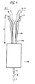
Figure 6 is a perspective view of a stamped terminal; -
Figure 7 is a perspective view of another stamped terminal; -
Figure 8 is a perspective view of a single contact assembly made in accordance with the invention; -
Figure 9 is a side view of the contact assembly ofFigure 8 ; -
Figure 10 is a perspective view of another single contact assembly made in accordance with the invention; and -
Figure 11 is a perspective view of a contact assembly in accordance with the invention mated with a pin. -
Figure 1 is a perspective view of a backplane system having an exemplary right angle electrical connector in accordance with an embodiment of the invention. However, the invention may take other forms such as a vertical or horizontal electrical connector. As shown inFigure 1 ,connector 100 comprises aplug 102 andreceptacle 1100. -
Plug 102 comprises ahousing 105 and a plurality oflead assemblies 108. Thehousing 105 is configured to contain and align the plurality oflead assemblies 108 such that an electrical connection suitable for signal communication is made between a firstelectrical device 112 and a secondelectrical device 110 viareceptacle 1100. In one embodiment of the invention,electrical device 110 is a backplane andelectrical device 112 is a daughtercard.Electrical devices - As shown, the
connector plug 102 comprises a plurality oflead assemblies 108. Eachlead assembly 108 comprises a column of terminals orconductors 130 therein as will be described below. Eachlead assembly 108 comprises any number ofterminals 130. -
Figure 1a is a board-to-board system similar toFigure 1 except plug connector 106 is a vertical plug connector rather than a right angle plug connector as shown inFigure 1 . This embodiment makes electrical connection between two parallelelectrical devices -
Figure 2 is a perspective view of theplug connector 102 ofFigure 1 shown withoutelectrical devices receptacle connector 1100. As shown,slots 107 are formed in thehousing 105 that contain and align thelead assemblies 108 therein. In one embodiment, thehousing 105 is made of plastic, however, any suitable material may be used without departing from the scope of the invention.Figure 2 also showsconnection pins Connection pins 130 connectconnector 102 toelectrical device 112.Connection pins 132 electrically connectconnector 102 toelectrical device 110 viareceptacle 1100.Connection pins 130 may be adapted to provide through-mount or surface-mount connections to an electrical device (not shown). -
Figure 3 is a side view ofplug connector 102 as shown inFIG. 2 . As shown, in this configuration, theterminals 132 used to connect toreceptacle 1100 vary in length, i.e. the terminals extend in varied lengths from the end of thehousing 105 from which theterminals 132 extend. For example, as shown,terminals 132B are ground terminals and extend a greater distance fromhousing 105 thanterminals 132A, which are signal terminals. During mating of theconnector plug 102 toreceptacle 1100, such configuration provides that thelonger ground terminals 132B onplug 102 will mate with the corresponding ground terminals on thereceptacle 1100 before theshorter signal terminals 132A mate with the corresponding signal terminals 1175A on thereceptacle 1100. Such a configuration can be used to ensure that signal integrity is maintained whenplug 102 is mated withreceptacle 1100. -
Figure 4 and5 are a perspective view and side view, respectively, of thereceptacle 1100 portion of the connector shown inFigure 1 . In this manner,receptacle 1100 may be mated with connector plug 102 (as shown inFigure 1 ) and used to connect two electrical devices (as shown inFigure 1 ). Specifically, connection pins orcontact terminals 133 may be inserted into, for example, vias (not shown) ondevice 110 to electrically connectconnector plug 102 todevice 110. In another embodiment of the invention, the connection pins 133 may be eye-of-the-needle pins for use in press-fit applications. -
Receptacle 1100 also includesalignment structures 1120 to aid in the alignment and insertion ofconnector plug 102 intoreceptacle 1100. Once inserted,structures 1120 also serve to secure the connector plug inreceptacle 1100.Such structures 1120 thereby resist any movement that may occur between the connector and receptacle that could result in mechanical breakage therebetween. -
Figure 6 is a perspective view of a stampedcontact terminal 60 manufactured using a process wherein tolerances are designed into the contact to provide a contact having a determined spring rate and gap. As shown, terminal 60 includes adual beam contact 63 on one end of the terminal 60 and an eye of theneedle configuration 62 on the other end of the terminal 60. In another embodiment of the invention, the eye of the needle configuration can be replaced with a straight pin configuration without departing from the scope of the invention.Terminal 60 also includes aprojection 64 for securing the terminal 60 in a contact block (not shown). - Dual
beam contact terminals 63 have a spring rate associated therewith. The spring rate of adual beam contact 63 is defined as how much force is required to deflect the beams of the contact a distance, is measured in force per unit distance, and is inversely proportional to the free length of the beam (While other factors effect spring rate, they are not relevant to this invention). For example, when a contact having a blade-like configuration (not-shown), is inserted intoterminal 60 in a direction as indicated by arrow C, the beams ofterminal 60 are deflected in a direction indicated by arrows F. Consequently, depending on the spring rate ofterminal 60, the force required to insert the blade-like contact (not shown) intoterminal 60 may vary. Generally, terminals in a connector must have a target normal force for proper mating with a complementary connector. - Dual
beam contact terminals 63 have a gap associated therewith. This gap is sized for the proper fitting of the terminal of the mating connector. The creation of this gap and its associated tolerances via stamping is a complex mechanical process. - The present invention can utilize dual beam contact terminals which are stamped with less restrictive tolerances and the resulting economy. In accordance with the present invention, the spring rate and the resultant normal force, is determined by the way the dual beam contact is inserted in the contact block (after the stamping operation). As mentioned above, the spring rate of a stamped beam is inversely proportional to the free length of the beam. Accordingly, once the stamped terminals are inserted into the contact block, as will be described in detail below, the spring rate can be adjusted by varying the free length of the beam protruding from the contact block, for example, by controlling the size and depth of the bore in the contact block.
- In accordance with the invention, a contact assembly for use in an electrical connector is provided that uses stamped terminals made without the stamping tolerances needed to produce a contact having a predetermined spring rate. In this manner, a contact assembly is provided that adjusts the contact's spring rate when inserting the contact into the contact block.
Figure 7 is a perspective view of a terminal stamped using a process without the tolerances as described above with respect to the prior art that still result in a stamped terminal having a pre-determined spring rate when inserted into the easily manufactured contact block. As shown, thedual beams 73 are relatively long and consequently would render a relatively high spring rate. Furthermore, because the contact block will be used to maintain the beam gap, the gap does not have to be held with tight tolerances in the terminal itself and therefore terminal 70 is less difficult and faster to manufacture. As a result, the terminal is less expensive to manufacture since the restrictive tolerances used to create the desired spring force and gap have been removed. -
Figure 8 and9 are a perspective and side view, respectively, of acontact assembly 80 in accordance with one aspect of the invention. In particular,Figure 8 and9 are used to illustrate how thecontact block 81 is used to adjust the spring rate of a non-tensioned stamped terminal in accordance with the invention. - Generally, it is desirable to maintain a contact force normal to the mating blade or
dual beams 83. For example, a minimum threshold contact force may be needed to make reliable contact (which may vary depending on the materials and shape). Also, a maximum threshold force may be needed to minimize the insertion force of multiple contact array connectors )(not shown). The desired contact force can be accomplished by using abeam 83 having a high spring rate and a short deflection or a beam with a low spring rate and a large deflection. A low spring rate is usually desirable as variation with tolerance is decreased. However, if the spring rate is too low, other mechanical constraints may prevent a very large deflection, rendering the contact unusable. - In accordance with the present invention, the spring rate is varied according to the length of the beams protruding above the contact block 81.As shown,
contact assembly 80 includescontact block 81 with asingle terminal 80A partially inserted within one of theapertures 82. Position A shows the beam before its length is dictated by its insertion in the contact block. As shown, partially insertedterminal 80A hasdual beams 83 at position A and dual beams have a spring rate A'. A given spring rate is created in this case, by varying the free length of the beams. For purposes of the disclosure, Applicants refer to this the force thecontact block 81 places on the beams as an inwardly directed tension. - As the terminal 80A is inserted further into
contact block 81 at direction indicated by arrow Z, the free-length of thebeam 83 decreases and thedual beams 83 move closer together due to the size of the bore in thecontact block 81. At position B, thebeams 83 have a spring rate B' associated thereat. Spring rate B' is typically greater than spring rate A' since, at position B, the dual beams have a smaller free length and therefore a greater inwardly directed tension in the direction of the arrow U created bycontact block 81. Position B is created if the beam is tensioned by thecontact block 81 to reduce the forces of mating while maintaining a satisfactory normal force. Therefore, when a mating contact (not shown) is inserted intodual beam contact 80A at a direction X, thedual beams 80A are deflected less of a distance due to the greater inwardly directed tension. - As
terminal 80A is inserted intocontact block 81 along a direction as indicated by arrow Z,dual beams 83 decrease even more in free length until they are seated at position C. Position C shows the beam in a position as defined by the aperture of thecontact block 81. Consequently, dual beams have a spring rate C' associated with position C withincontact block 81. Typically, spring rate C' is greater than spring rate B' since, at position C, thedual beams 83 have a greater inwardly directed tension created bycontact block 81. Therefore, when a contact (not shown) is inserted intodual beam contact 80A at a direction X, thedual beams 80A are deflected less of distance due to the greater inwardly directed tension. In one embodiment, spring rate C' is defined by a customer specification. Therefore, the spring rate of dualbeam contact terminals 83 may be adjusted by inserting thecontact 83 varying distances into thecontact block 81 to control their amount of free length. - Also, the
terminals 80A can be inserted into thecontact block 81 such that thedual beams 83 have a desired beam gap once seated incontact block 81. The beam gap is the distance between the dual beam contact terminals at a common point. For example, as shown inFigure 11 , the beam gap is the distance between the dual beam contact terminals at the point furthest from thecontact block 1081. In this manner, the beam gap between the dual beams can be adjusted by adjusting the diameter D of theaperture 82 in the contact block. The beam gap may vary, for example, depending on the size of a complementary contact used in mating. - Furthermore, in accordance with another aspect of the invention, the beam height or length of the terminal can be adjusted. The beam height or length (another name for free length) is a value that reflects how far the beam extends from the
contact block 81. As shown inFigure 9 , the beam height H is the distance between the distal end of the beam and the contact block. The beam height H, therefore, can be adjusted by inserting the terminal 80A into contact block at varying distances. The beam height can be adjusted to meet engineering or customer specifications or the like without departing from the scope of the invention. - As stated above, by adjusting the beam height, the spring rate of the dual beam contact may also be adjusted. As such, the terminals can be inserted into the
contact block 81 such that the dual beams have a desired spring rate. The desired spring rate may be any spring rate. In a preferred embodiment, the spring rate is any rate that is suitable such that the dual beams may properly mate with a complementary connector. - The spring rate of terminal 80A is related to the beam height, which, for example can be measured from the fulcrum point F. In the embodiment shown in
Figure 8 , the fulcrum point F is the uppermost point ofcontact block 81 where the terminal 80A contacts the contact block 1168 and serves as the fulcrum when a mating contact is inserted (in the direction indicated by arrow Z) into the dual beam ground contact. By adjusting the beam height, the spring rate of terminal 80A can be adjusted to a desired value, for example, according to a supplied customer specification. - Referring now to
Figure 10 , acontact assembly 1080 in accordance with the invention is shown. In this manner and as shown, the contact assembly of the invention includes eight stamped dual beam contact terminals, such as that shown inFigure 7 , i.e. one manufactured without a predetermined spring rate, in an electrical connector, yet still have a desired spring rate once installed incontact block 1081. The contact assembly may include any number of terminals without departing from the invention. - As shown in
Figure 10 ,contact assembly 1080 includes acontact block 1081. Thecontact block 1081 is typically made from an insulating material. In one embodiment, thecontact block 81 is manufactured using injection molding, however, other processes may be used without departing from the scope of the invention. In general, however, the manufacturing processes and costs related to the manufacturing of the contact block are less than those that would be related to the stamping of a highly-toleranced dual beam contact according to the prior art. -
Contact block 1081 includes a plurality ofapertures 1082 therethrough, each aperture defined byaperture sidewalls 1082C. Furthermore, eachaperture 1082 has a diameter D that can be used to tension the terminal 1080A to a determined spring rate. -
Contact block 1081 also includes containsterminals 1080A, each terminal 1080A seated within anaperture 1082. As shown,terminals 1080A include dualbeam contact terminals 1083 for mating with a complementary contact. For example, dualbeam contact terminals 1083 may mate with a contact having a blade configuration. - In accordance with one aspect of the invention,
terminals 1080A are positioned incontact block 1081 such that, once seated within thecontact block 1081, the previously non-tensioned terminals become pre-loaded or tensioned in an inward direction arrow, U, such inward tension is opposed to the tendency of dual beams to move in a direction opposite of arrow T. In other words, the structure ofcontact block 1081 prevents dualbeam contact terminals 1083 from moving in a direction indicated by arrow T. - In accordance with another aspect of the invention, the dual
beam contact terminals 1083 are seated inbeam seats aperture 1082. Beam seats are cavities formed within theaperture sidewall 1082C and secure dualbeam contact terminals 1083 from any lateral movement once positioned in theaperture 1082 withincontact block 1081. Also, beam seats can be used to align thedual beams 1083. As such, the tolerances required to stamp terminals having a precise alignment are reduced. Consequently, manufacturing costs are also reduced. As shown, aperture seats are rectangular in shape, however, any shape may be used without departing from the scope of the invention. -
Figure 11 is a perspective view of a contact assembly in accordance with the invention mated with a pin. As shown, a mating contact orpin 1290 having a bladed configuration is inserted intodual beam contact 1283 in a direction indicated by arrow I. Once inserted, thedual beams 1283 are deflected in a direction indicated by arrow G. - In accordance with another aspect of the invention, the
mating contact 1290 is not limited to the beam height or cantilevered length of terminal 1280A. In this manner, by adjusting the depth of terminal in thecontact block 1281, the insertion depth Di of the mating contact can also be adjusted. The insertion depth can be adjusted to allow for contact wipe. Contact wipe is a deviation parameter used to allow for curvatures that may exist in an electrical device that results in non-simultaneous contact mating when connectors are mated. In this manner, increasing the insertion depth allows for greater contact wipe. - It is to be understood that the foregoing illustrative embodiments have been provided merely for the purpose of explanation and are in no way to be construed as limiting of the invention. Words which have been used herein are words of description and illustration, rather than words of limitation. Further, although the invention has been described herein with reference to particular structure, materials and/or embodiments, the invention is not intended to be limited to the particulars disclosed herein. Rather, the invention extends to all functionally equivalent structures, methods and uses, such as are within the scope of the appended claims.
Claims (17)
- A contact assembly for use in an electrical connector (100) comprising: an insulative contact block (81, 1081, 1281) defining a plurality of apertures (82, 1082, 1282) therethrough; and a plurality of dual beam contact terminals (63, 73, 83, 1083, 1283), each terminal extending through an aperture in the contact block (81), characterized in that each dual beam contact (63, 73, 83, 1083, 1283) is seated within one of the plurality of apertures of the contact block (81, 1081, 1281) at an inwardly directed tension (U) such that the contact block (81) maintains a desired spring rate on each dual beam contact (63, 73, 83, 1083, 1283), each dual beam contact (63, 73, 83, 1083, 1283) extends a length from the contact block (81, 1081, 1281), and the desired spring rate of each dual beam contact can be adjusted by varying the length.
- The contact assembly of claim 1, wherein said plurality of apertures (82, 1082, 1282) each have sidewalls and the sidewalls define beam seats (82A, 82B, 1082A, 1082B) adapted to secure the beams of each contact.
- The contact assembly of claim 1 wherein each aperture (82, 1082, 1282) is sized to provide a desired beam gap.
- The contact assembly of claim 1 wherein each of the plurality of terminals (60, 70) includes a projection (64, 74) thereon for securing the contact to the contact block.
- The contact assembly of claim 1 wherein each opposing beam in each of said dual beam contact terminals (63, 73, 83, 1083, 1283) is spaced to achieve a desired normal force.
- A receptacle comprising:a housing (105); anda plurality of contact assemblies as set forth in any one of claims 1 to 5 contained in the housing (105).
- The receptacle of claim 6, wherein said plurality of apertures each have sidewalls (1082C) and the sidewalls (1082C) define beam seats (1082A, 1082B) adapted to secure the beams of each contact.
- The receptacle of claim 6, wherein each aperture (82, 1082) is sized to provide a desired beam gap.
- The receptacle of claim 6, wherein each dual beam contact (63, 73, 83, 1083, 1283) extends a length from the contact block and further wherein the desired spring rate of each dual beam can be adjusted by varying the length.
- The receptacle of claim 6 wherein each opposing beam in each of said dual beam contact terminals (63, 73, 83, 1083, 1283) is spaced to achieve a desired normal force.
- The receptacle of claim 6 wherein each of the plurality of terminals (60, 70) includes a projection (64, 74) thereon for securing the contact to the contact block.
- An electrical connector comprising:a plug connector (102); anda receptacle (1100) electrically connectable to the plug connector (102) comprising:a housing (105); anda plurality of contact assemblies as set forth in any one of claims 1 to 5 contained in the housing (105).
- The electrical connector of claim 12, wherein said plurality of apertures (1082) each have sidewalls (1082C) and the sidewalls (1082C) define beam seats (1082A, 1082B) adapted to secure the beams of each contact.
- The electrical connector of claim 12 wherein each aperture (1082) is sized to provide a desired beam gap.
- The electrical connector of claim 12 wherein each of the plurality of terminals (60, 70) includes a projection (64, 74) thereon for securing the contact to the contact block.
- A method for making a contact assembly comprising:providing an insulative contact block (81, 1081, 1281) having a plurality of apertures therethrough; and inserting a dual beam contact terminal into one of said plurality of apertures (82, 1082, 1282) further characterized in that each dual beam configuration is seated within one of the plurality of apertures (82, 1082, 1282) of the contact block (81, 1081, 1281) at an inwardly directed tension (U) such that the contact block maintains a desired spring rate on the dual beam, each dual beam contact (63, 73, 83, 1083, 1283) extends a length from the contact block (81, 1081, 1281), and the desired spring rate of each dual beam contact can be adjusted by varying the length.
- The method of claim 16 further comprising:inserting the contact terminal (83, 1083, 1283) into one of said plurality of apertures (82, 1082, 1282) such that the dual beam exhibits a desired beam gap.
Applications Claiming Priority (3)
| Application Number | Priority Date | Filing Date | Title |
|---|---|---|---|
| US232353 | 1988-08-15 | ||
| US10/232,353 US7008250B2 (en) | 2002-08-30 | 2002-08-30 | Connector receptacle having a short beam and long wipe dual beam contact |
| PCT/US2003/027364 WO2004021515A2 (en) | 2002-08-30 | 2003-08-29 | Connector receptacle having a short beam and long wipe dual beam contact |
Publications (3)
| Publication Number | Publication Date |
|---|---|
| EP1535367A2 EP1535367A2 (en) | 2005-06-01 |
| EP1535367A4 EP1535367A4 (en) | 2007-03-28 |
| EP1535367B1 true EP1535367B1 (en) | 2013-10-23 |
Family
ID=31976985
Family Applications (1)
| Application Number | Title | Priority Date | Filing Date |
|---|---|---|---|
| EP03770276.8A Expired - Lifetime EP1535367B1 (en) | 2002-08-30 | 2003-08-29 | Connector receptacle having a short beam and long wipe dual beam contact |
Country Status (6)
| Country | Link |
|---|---|
| US (2) | US7008250B2 (en) |
| EP (1) | EP1535367B1 (en) |
| JP (1) | JP2005537615A (en) |
| CN (1) | CN100440629C (en) |
| AU (1) | AU2003278752A1 (en) |
| WO (1) | WO2004021515A2 (en) |
Families Citing this family (28)
| Publication number | Priority date | Publication date | Assignee | Title |
|---|---|---|---|---|
| US7462924B2 (en) * | 2006-06-27 | 2008-12-09 | Fci Americas Technology, Inc. | Electrical connector with elongated ground contacts |
| US7462053B2 (en) * | 2006-07-03 | 2008-12-09 | Hon Hai Precision Ind. Co., Ltd. | Electrical contact and process for making the same and connector comprising the same |
| EP2127035A2 (en) * | 2006-12-20 | 2009-12-02 | Amphenol Corporation | Electrical connector assembly |
| BRPI0700018A (en) * | 2007-01-09 | 2008-08-26 | 3M Innovative Properties Co | power distribution bus connector set and power distribution method using the same |
| US7604519B2 (en) * | 2007-05-10 | 2009-10-20 | Hon Hai Precision Ind. Co., Ltd. | Connector assembly with improved contacts |
| US8469720B2 (en) | 2008-01-17 | 2013-06-25 | Amphenol Corporation | Electrical connector assembly |
| US7883366B2 (en) * | 2009-02-02 | 2011-02-08 | Tyco Electronics Corporation | High density connector assembly |
| US8550861B2 (en) | 2009-09-09 | 2013-10-08 | Amphenol TCS | Compressive contact for high speed electrical connector |
| US20110059652A1 (en) * | 2009-09-10 | 2011-03-10 | Amphenol Corporation | Multi-pathway connector for circuit boards |
| US8657616B2 (en) * | 2011-05-24 | 2014-02-25 | Fci Americas Technology Llc | Electrical contact normal force increase |
| WO2013119529A1 (en) | 2012-02-07 | 2013-08-15 | 3M Innovative Properties Company | Electrical connector strain relief |
| EP2812953A4 (en) | 2012-02-07 | 2015-10-07 | 3M Innovative Properties Co | Electrical connector contact terminal |
| JP6073373B2 (en) | 2012-02-07 | 2017-02-01 | スリーエム イノベイティブ プロパティズ カンパニー | Wire mount electrical connector |
| US9509094B2 (en) | 2012-02-07 | 2016-11-29 | 3M Innovative Properties Company | Board mount electrical connector with latch opening on bottom wall |
| CN104321936B (en) | 2012-02-07 | 2018-04-24 | 3M创新有限公司 | Electric connector breech lock |
| US8771018B2 (en) | 2012-05-24 | 2014-07-08 | Tyco Electronics Corporation | Card edge connector |
| WO2015095869A1 (en) * | 2013-12-20 | 2015-06-25 | Molex Incorporated | Connector with tuned terminal beam |
| JP6744835B2 (en) * | 2017-03-31 | 2020-08-19 | モレックス エルエルシー | connector |
| CN108448292B (en) * | 2018-05-15 | 2024-10-22 | 深圳市益晟康科技有限公司 | Electrical connector |
| US11637391B2 (en) | 2020-03-13 | 2023-04-25 | Amphenol Commercial Products (Chengdu) Co., Ltd. | Card edge connector with strength member, and circuit board assembly |
| US11973286B2 (en) | 2020-06-01 | 2024-04-30 | Amphenol Commercial Products (Chengdu) Co., Ltd. | Electrical connector and manufacturing method thereof |
| US11710923B2 (en) | 2020-07-31 | 2023-07-25 | Amphenol Commercial Products (Chengdu) Co., Ltd. | Compact, reliable card edge connector |
| CN212874843U (en) | 2020-08-31 | 2021-04-02 | 安费诺商用电子产品(成都)有限公司 | electrical connector |
| CN114597707A (en) | 2020-12-04 | 2022-06-07 | 安费诺商用电子产品(成都)有限公司 | Card edge connector with locking system |
| US12431644B2 (en) | 2021-09-24 | 2025-09-30 | Amphenol Commercial Products (Chengdu) Co., Ltd. | Electrical connector for compact system |
| CN216488833U (en) | 2021-10-27 | 2022-05-10 | 安费诺商用电子产品(成都)有限公司 | electrical connector |
| TW202327191A (en) | 2021-11-22 | 2023-07-01 | 大陸商安費諾商用電子產品(成都)有限公司 | Robust electrical connector |
| US12463363B2 (en) | 2021-12-06 | 2025-11-04 | Amphenol Commercial Products (Chengdu) Co., Ltd. | Reliable electrical connector |
Family Cites Families (110)
| Publication number | Priority date | Publication date | Assignee | Title |
|---|---|---|---|---|
| US3115379A (en) | 1961-11-29 | 1963-12-24 | United Carr Fastener Corp | Electrical connector |
| US3286220A (en) * | 1964-06-10 | 1966-11-15 | Amp Inc | Electrical connector means |
| US3538486A (en) * | 1967-05-25 | 1970-11-03 | Amp Inc | Connector device with clamping contact means |
| US3669054A (en) | 1970-03-23 | 1972-06-13 | Amp Inc | Method of manufacturing electrical terminals |
| US3704441A (en) * | 1970-08-03 | 1972-11-28 | Amp Inc | Panel mounted electrical terminal |
| US3731252A (en) * | 1971-03-22 | 1973-05-01 | Bendix Corp | Printed circuit board connector |
| US3748633A (en) | 1972-01-24 | 1973-07-24 | Amp Inc | Square post connector |
| US4004845A (en) * | 1975-04-17 | 1977-01-25 | Elco Corporation | High density electrical connector employing male blade with offset portions |
| US4140361A (en) * | 1975-06-06 | 1979-02-20 | Sochor Jerzy R | Flat receptacle contact for extremely high density mounting |
| US4076362A (en) * | 1976-02-20 | 1978-02-28 | Japan Aviation Electronics Industry Ltd. | Contact driver |
| US4159861A (en) * | 1977-12-30 | 1979-07-03 | International Telephone And Telegraph Corporation | Zero insertion force connector |
| US4288139A (en) | 1979-03-06 | 1981-09-08 | Amp Incorporated | Trifurcated card edge terminal |
| US4260212A (en) | 1979-03-20 | 1981-04-07 | Amp Incorporated | Method of producing insulated terminals |
| NL8003228A (en) * | 1980-06-03 | 1982-01-04 | Du Pont Nederland | BRIDGE CONTACT FOR THE ELECTRICAL CONNECTION OF TWO PINS. |
| US4402563A (en) * | 1981-05-26 | 1983-09-06 | Aries Electronics, Inc. | Zero insertion force connector |
| US4480888A (en) * | 1982-06-23 | 1984-11-06 | Amp Incorporated | Multi terminal low insertion force connector |
| US4560222A (en) * | 1984-05-17 | 1985-12-24 | Molex Incorporated | Drawer connector |
| US4607907A (en) | 1984-08-24 | 1986-08-26 | Burndy Corporation | Electrical connector requiring low mating force |
| NL8502046A (en) * | 1985-07-16 | 1987-02-16 | Du Pont Nederland | ELECTRIC CONTACTS FOR CIRCUIT BOARD. |
| US4618199A (en) * | 1985-08-30 | 1986-10-21 | Pfaff Wayne | Low insertion force socket |
| US4717360A (en) * | 1986-03-17 | 1988-01-05 | Zenith Electronics Corporation | Modular electrical connector |
| US4684193A (en) * | 1986-08-08 | 1987-08-04 | Havel Karel | Electrical zero insertion force multiconnector |
| US4964814A (en) * | 1986-10-03 | 1990-10-23 | Minnesota Mining And Manufacturing Co. | Shielded and grounded connector system for coaxial cables |
| US4776803A (en) | 1986-11-26 | 1988-10-11 | Minnesota Mining And Manufacturing Company | Integrally molded card edge cable termination assembly, contact, machine and method |
| CA1285036C (en) * | 1986-12-26 | 1991-06-18 | Kyoichiro Kawano | Electrical connector |
| KR910001862B1 (en) * | 1987-02-24 | 1991-03-28 | 가부시끼가이샤 도시바 | Connector |
| CH675929A5 (en) * | 1988-05-06 | 1990-11-15 | Cdm Connectors Dev & Mfg Ag | |
| US4907990A (en) * | 1988-10-07 | 1990-03-13 | Molex Incorporated | Elastically supported dual cantilever beam pin-receiving electrical contact |
| US4878861A (en) * | 1988-11-01 | 1989-11-07 | Elfab Corporation | Compliant electrical connector pin |
| JPH02199780A (en) * | 1989-01-30 | 1990-08-08 | Yazaki Corp | Low insertion force terminal |
| US5077893A (en) | 1989-09-26 | 1992-01-07 | Molex Incorporated | Method for forming electrical terminal |
| ES2070283T3 (en) * | 1989-10-10 | 1995-06-01 | Whitaker Corp | CONTRAPLANE CONNECTOR WITH ADAPTED IMPEDANCES. |
| JP2739608B2 (en) * | 1990-11-15 | 1998-04-15 | 日本エー・エム・ピー株式会社 | Multi-contact type connector for signal transmission |
| JP2583839B2 (en) * | 1991-07-24 | 1997-02-19 | ヒロセ電機株式会社 | High speed transmission electrical connector |
| US5487684A (en) * | 1992-07-01 | 1996-01-30 | Berg Technology, Inc. | Electrical contact pin for printed circuit board |
| US5254012A (en) * | 1992-08-21 | 1993-10-19 | Industrial Technology Research Institute | Zero insertion force socket |
| JP3161642B2 (en) * | 1992-12-18 | 2001-04-25 | 富士通株式会社 | Connector and method of assembling the same |
| JP2684502B2 (en) | 1993-01-12 | 1997-12-03 | 日本航空電子工業株式会社 | socket |
| US5302135A (en) * | 1993-02-09 | 1994-04-12 | Lee Feng Jui | Electrical plug |
| JP3108239B2 (en) * | 1993-02-19 | 2000-11-13 | 富士通株式会社 | Impedance matched electrical connector |
| US5274918A (en) | 1993-04-15 | 1994-01-04 | The Whitaker Corporation | Method for producing contact shorting bar insert for modular jack assembly |
| FR2710463B1 (en) | 1993-09-20 | 1995-11-10 | Alcatel Cable Interface | Hermaphroditic contact and connection defined by a pair of such contacts. |
| JP2764687B2 (en) | 1993-10-18 | 1998-06-11 | 日本航空電子工業株式会社 | High-speed transmission connector |
| US5403215A (en) * | 1993-12-21 | 1995-04-04 | The Whitaker Corporation | Electrical connector with improved contact retention |
| US5431578A (en) * | 1994-03-02 | 1995-07-11 | Abrams Electronics, Inc. | Compression mating electrical connector |
| US5564954A (en) * | 1995-01-09 | 1996-10-15 | Wurster; Woody | Contact with compliant section |
| US5573431A (en) * | 1995-03-13 | 1996-11-12 | Wurster; Woody | Solderless contact in board |
| JP3075462B2 (en) * | 1995-03-27 | 2000-08-14 | 矢崎総業株式会社 | Connector with straight terminal fittings |
| US5609502A (en) | 1995-03-31 | 1997-03-11 | The Whitaker Corporation | Contact retention system |
| US5580257A (en) * | 1995-04-28 | 1996-12-03 | Molex Incorporated | High performance card edge connector |
| US5817973A (en) * | 1995-06-12 | 1998-10-06 | Berg Technology, Inc. | Low cross talk and impedance controlled electrical cable assembly |
| TW267265B (en) * | 1995-06-12 | 1996-01-01 | Connector Systems Tech Nv | Low cross talk and impedance controlled electrical connector |
| US5961191A (en) * | 1995-06-22 | 1999-10-05 | Taylor; Charles M. | Picnic caddy |
| US5590463A (en) | 1995-07-18 | 1997-01-07 | Elco Corporation | Circuit board connectors |
| US5558542A (en) * | 1995-09-08 | 1996-09-24 | Molex Incorporated | Electrical connector with improved terminal-receiving passage means |
| US5971817A (en) * | 1995-09-27 | 1999-10-26 | Siemens Aktiengesellschaft | Contact spring for a plug-in connector |
| US5741161A (en) * | 1996-01-04 | 1998-04-21 | Pcd Inc. | Electrical connection system with discrete wire interconnections |
| US5676570A (en) | 1996-03-15 | 1997-10-14 | Minnesota Mining And Manufacturing Company | "F" port interface connector |
| US6056590A (en) | 1996-06-25 | 2000-05-02 | Fujitsu Takamisawa Component Limited | Connector having internal switch and fabrication method thereof |
| US5761050A (en) * | 1996-08-23 | 1998-06-02 | Cts Corporation | Deformable pin connector for multiple PC boards |
| US5795191A (en) | 1996-09-11 | 1998-08-18 | Preputnick; George | Connector assembly with shielded modules and method of making same |
| US6139336A (en) * | 1996-11-14 | 2000-10-31 | Berg Technology, Inc. | High density connector having a ball type of contact surface |
| JP3509444B2 (en) | 1997-01-13 | 2004-03-22 | 住友電装株式会社 | Insert molding connector |
| US5993259A (en) * | 1997-02-07 | 1999-11-30 | Teradyne, Inc. | High speed, high density electrical connector |
| US5980321A (en) * | 1997-02-07 | 1999-11-09 | Teradyne, Inc. | High speed, high density electrical connector |
| CN2292338Y (en) * | 1997-03-06 | 1998-09-23 | 鸿海精密工业股份有限公司 | Substrate buckle device for electrical connector |
| US6068520A (en) | 1997-03-13 | 2000-05-30 | Berg Technology, Inc. | Low profile double deck connector with improved cross talk isolation |
| JP3379747B2 (en) * | 1997-05-20 | 2003-02-24 | 矢崎総業株式会社 | Low insertion force terminal |
| US6146157A (en) | 1997-07-08 | 2000-11-14 | Framatome Connectors International | Connector assembly for printed circuit boards |
| US5908333A (en) * | 1997-07-21 | 1999-06-01 | Rambus, Inc. | Connector with integral transmission line bus |
| JP3269436B2 (en) * | 1997-09-19 | 2002-03-25 | 株式会社村田製作所 | Manufacturing method of insert resin molded product |
| US6227882B1 (en) * | 1997-10-01 | 2001-05-08 | Berg Technology, Inc. | Connector for electrical isolation in a condensed area |
| US5961355A (en) * | 1997-12-17 | 1999-10-05 | Berg Technology, Inc. | High density interstitial connector system |
| DE19829467C2 (en) | 1998-07-01 | 2003-06-18 | Amphenol Tuchel Elect | Contact carrier especially for a thin smart card connector |
| WO1999037466A1 (en) * | 1998-01-21 | 1999-07-29 | Teijin Limited | Biaxially oriented polyester film for membrane switch |
| US6155860A (en) * | 1998-01-31 | 2000-12-05 | Berg Technology, Inc. | Socket for electrical component |
| US5980271A (en) * | 1998-04-15 | 1999-11-09 | Hon Hai Precision Ind. Co., Ltd. | Header connector of a future bus and related compliant pins |
| US6319075B1 (en) * | 1998-04-17 | 2001-11-20 | Fci Americas Technology, Inc. | Power connector |
| JP2000003744A (en) | 1998-06-15 | 2000-01-07 | Honda Tsushin Kogyo Co Ltd | Printed circuit board connector |
| JP2000003745A (en) | 1998-06-15 | 2000-01-07 | Honda Tsushin Kogyo Co Ltd | Printed circuit board connector |
| JP3755989B2 (en) | 1998-06-15 | 2006-03-15 | 本多通信工業株式会社 | PCB connector |
| JP2000003746A (en) | 1998-06-15 | 2000-01-07 | Honda Tsushin Kogyo Co Ltd | Printed circuit board connector |
| JP3361757B2 (en) * | 1998-10-29 | 2003-01-07 | 第一電子工業株式会社 | Press-in contact |
| TW393812B (en) | 1998-12-24 | 2000-06-11 | Hon Hai Prec Ind Co Ltd | A manufacturing method of high-density electrical connector and its product |
| TW445679B (en) | 1998-12-31 | 2001-07-11 | Hon Hai Prec Ind Co Ltd | Method for manufacturing modular terminals of electrical connector |
| US6220896B1 (en) * | 1999-05-13 | 2001-04-24 | Berg Technology, Inc. | Shielded header |
| US6123554A (en) * | 1999-05-28 | 2000-09-26 | Berg Technology, Inc. | Connector cover with board stiffener |
| JP2000340324A (en) * | 1999-05-31 | 2000-12-08 | Enplas Corp | Socket for electric component |
| JP3397303B2 (en) | 1999-06-17 | 2003-04-14 | エヌイーシートーキン株式会社 | Connector and manufacturing method thereof |
| JP2001102131A (en) * | 1999-10-01 | 2001-04-13 | Sumitomo Wiring Syst Ltd | Connector |
| DE10051819A1 (en) | 1999-10-18 | 2001-04-19 | Erni Elektroapp | Multipole, single- or multi-row plug connector of blade and spring type e.g. for circuit boards, comprises screen consisting of screen group with first element located in blade strip |
| EP1232540B1 (en) | 1999-11-24 | 2009-10-28 | Amphenol Corporation | Differential signal electrical connectors |
| US6293827B1 (en) * | 2000-02-03 | 2001-09-25 | Teradyne, Inc. | Differential signal electrical connector |
| TW444940U (en) * | 2000-03-03 | 2001-07-01 | Molex Inc | Battery connector |
| US6371773B1 (en) * | 2000-03-23 | 2002-04-16 | Ohio Associated Enterprises, Inc. | High density interconnect system and method |
| DE10027125A1 (en) * | 2000-05-31 | 2001-12-06 | Wabco Gmbh & Co Ohg | Electrical plug contact |
| US6350134B1 (en) * | 2000-07-25 | 2002-02-26 | Tyco Electronics Corporation | Electrical connector having triad contact groups arranged in an alternating inverted sequence |
| US6409543B1 (en) * | 2001-01-25 | 2002-06-25 | Teradyne, Inc. | Connector molding method and shielded waferized connector made therefrom |
| US6461202B2 (en) * | 2001-01-30 | 2002-10-08 | Tyco Electronics Corporation | Terminal module having open side for enhanced electrical performance |
| US6386914B1 (en) * | 2001-03-26 | 2002-05-14 | Amphenol Corporation | Electrical connector having mixed grounded and non-grounded contacts |
| US6506081B2 (en) * | 2001-05-31 | 2003-01-14 | Tyco Electronics Corporation | Floatable connector assembly with a staggered overlapping contact pattern |
| US6431914B1 (en) * | 2001-06-04 | 2002-08-13 | Hon Hai Precision Ind. Co., Ltd. | Grounding scheme for a high speed backplane connector system |
| US6435914B1 (en) * | 2001-06-27 | 2002-08-20 | Hon Hai Precision Ind. Co., Ltd. | Electrical connector having improved shielding means |
| US6454575B1 (en) * | 2001-09-14 | 2002-09-24 | Hon Hai Precision Ind. Co., Ltd. | Power plug connector having press-fit contacts |
| US6692272B2 (en) * | 2001-11-14 | 2004-02-17 | Fci Americas Technology, Inc. | High speed electrical connector |
| US6652318B1 (en) * | 2002-05-24 | 2003-11-25 | Fci Americas Technology, Inc. | Cross-talk canceling technique for high speed electrical connectors |
| US6454615B1 (en) * | 2001-12-07 | 2002-09-24 | Hon Hai Precision Ind. Co., Ltd. | High-speed electrical connector |
| US6899566B2 (en) * | 2002-01-28 | 2005-05-31 | Erni Elektroapparate Gmbh | Connector assembly interface for L-shaped ground shields and differential contact pairs |
| US6572410B1 (en) * | 2002-02-20 | 2003-06-03 | Fci Americas Technology, Inc. | Connection header and shield |
| US6808420B2 (en) * | 2002-05-22 | 2004-10-26 | Tyco Electronics Corporation | High speed electrical connector |
-
2002
- 2002-08-30 US US10/232,353 patent/US7008250B2/en not_active Expired - Lifetime
-
2003
- 2003-08-29 EP EP03770276.8A patent/EP1535367B1/en not_active Expired - Lifetime
- 2003-08-29 CN CNB038179253A patent/CN100440629C/en not_active Expired - Fee Related
- 2003-08-29 JP JP2004532038A patent/JP2005537615A/en not_active Withdrawn
- 2003-08-29 WO PCT/US2003/027364 patent/WO2004021515A2/en not_active Ceased
- 2003-08-29 AU AU2003278752A patent/AU2003278752A1/en not_active Abandoned
-
2005
- 2005-11-22 US US11/285,409 patent/US7182616B2/en not_active Expired - Lifetime
Also Published As
| Publication number | Publication date |
|---|---|
| EP1535367A4 (en) | 2007-03-28 |
| WO2004021515A2 (en) | 2004-03-11 |
| AU2003278752A1 (en) | 2004-03-19 |
| CN100440629C (en) | 2008-12-03 |
| WO2004021515A3 (en) | 2004-04-29 |
| CN1672298A (en) | 2005-09-21 |
| US20060073724A1 (en) | 2006-04-06 |
| EP1535367A2 (en) | 2005-06-01 |
| JP2005537615A (en) | 2005-12-08 |
| AU2003278752A8 (en) | 2004-03-19 |
| US20040043672A1 (en) | 2004-03-04 |
| US7182616B2 (en) | 2007-02-27 |
| US7008250B2 (en) | 2006-03-07 |
Similar Documents
| Publication | Publication Date | Title |
|---|---|---|
| EP1535367B1 (en) | Connector receptacle having a short beam and long wipe dual beam contact | |
| US7270573B2 (en) | Electrical connector with load bearing features | |
| US7396259B2 (en) | Electrical connector housing alignment feature | |
| US6899548B2 (en) | Electrical connector having a cored contact assembly | |
| US5692928A (en) | Electrical connector having terminals with improved retention means | |
| EP0846350B1 (en) | Method for making surface mountable connectors | |
| US10230192B2 (en) | Electrical connector | |
| US5080596A (en) | Connector with contact spacer plate providing greater lateral force on rear contacts | |
| EP0472006A1 (en) | Electrical terminal with means to insure that a positive electrical connection is effected | |
| US4795374A (en) | Double sided edge connector | |
| KR102845338B1 (en) | Electric connector for circuit board and electric connector assembly | |
| EP0740372B1 (en) | Electrical connector | |
| EP0657959B1 (en) | Electrical connector assembly for mounting on a printed circuit board | |
| US5672084A (en) | High density connector receptacle | |
| EP0488349B1 (en) | Connector with contact spacer plate having tapered channels | |
| EP0806813B1 (en) | Electrical connector having terminals with improved retention means | |
| EP0079665B1 (en) | Connector housing | |
| CN113270774B (en) | Shorting pin, plug connector with such a shorting pin, and method for producing such a shorting pin | |
| US20110111641A1 (en) | Connector | |
| KR20020004853A (en) | Electrical connector assembly |
Legal Events
| Date | Code | Title | Description |
|---|---|---|---|
| PUAI | Public reference made under article 153(3) epc to a published international application that has entered the european phase |
Free format text: ORIGINAL CODE: 0009012 |
|
| 17P | Request for examination filed |
Effective date: 20050107 |
|
| AK | Designated contracting states |
Kind code of ref document: A2 Designated state(s): AT BE BG CH CY CZ DE DK EE ES FI FR GB GR HU IE IT LI LU MC NL PT RO SE SI SK TR |
|
| AX | Request for extension of the european patent |
Extension state: AL LT LV MK |
|
| RAP1 | Party data changed (applicant data changed or rights of an application transferred) |
Owner name: FCI |
|
| DAX | Request for extension of the european patent (deleted) | ||
| 111Z | Information provided on other rights and legal means of execution |
Free format text: ATBEBGCHCYCZDEDKEEESFIFRGBGRHUIEITLUMCNLPTROSESISKTR Effective date: 20060213 |
|
| A4 | Supplementary search report drawn up and despatched |
Effective date: 20070228 |
|
| RAP1 | Party data changed (applicant data changed or rights of an application transferred) |
Owner name: FCI |
|
| 17Q | First examination report despatched |
Effective date: 20110518 |
|
| REG | Reference to a national code |
Ref country code: DE Ref legal event code: R079 Ref document number: 60345158 Country of ref document: DE Free format text: PREVIOUS MAIN CLASS: H01R0013400000 Ipc: H01R0013110000 |
|
| GRAP | Despatch of communication of intention to grant a patent |
Free format text: ORIGINAL CODE: EPIDOSNIGR1 |
|
| INTG | Intention to grant announced |
Effective date: 20130517 |
|
| RIC1 | Information provided on ipc code assigned before grant |
Ipc: H01R 13/11 20060101AFI20130506BHEP Ipc: H01R 12/58 20110101ALI20130506BHEP |
|
| GRAS | Grant fee paid |
Free format text: ORIGINAL CODE: EPIDOSNIGR3 |
|
| GRAA | (expected) grant |
Free format text: ORIGINAL CODE: 0009210 |
|
| AK | Designated contracting states |
Kind code of ref document: B1 Designated state(s): AT BE BG CH CY CZ DE DK EE ES FI FR GB GR HU IE IT LI LU MC NL PT RO SE SI SK TR |
|
| REG | Reference to a national code |
Ref country code: GB Ref legal event code: FG4D |
|
| REG | Reference to a national code |
Ref country code: CH Ref legal event code: EP |
|
| REG | Reference to a national code |
Ref country code: AT Ref legal event code: REF Ref document number: 638011 Country of ref document: AT Kind code of ref document: T Effective date: 20131115 |
|
| REG | Reference to a national code |
Ref country code: IE Ref legal event code: FG4D |
|
| REG | Reference to a national code |
Ref country code: DE Ref legal event code: R096 Ref document number: 60345158 Country of ref document: DE Effective date: 20131219 |
|
| REG | Reference to a national code |
Ref country code: RO Ref legal event code: EPE |
|
| REG | Reference to a national code |
Ref country code: NL Ref legal event code: VDEP Effective date: 20131023 |
|
| REG | Reference to a national code |
Ref country code: AT Ref legal event code: MK05 Ref document number: 638011 Country of ref document: AT Kind code of ref document: T Effective date: 20131023 |
|
| PG25 | Lapsed in a contracting state [announced via postgrant information from national office to epo] |
Ref country code: BE Free format text: LAPSE BECAUSE OF FAILURE TO SUBMIT A TRANSLATION OF THE DESCRIPTION OR TO PAY THE FEE WITHIN THE PRESCRIBED TIME-LIMIT Effective date: 20131023 Ref country code: FI Free format text: LAPSE BECAUSE OF FAILURE TO SUBMIT A TRANSLATION OF THE DESCRIPTION OR TO PAY THE FEE WITHIN THE PRESCRIBED TIME-LIMIT Effective date: 20131023 Ref country code: SE Free format text: LAPSE BECAUSE OF FAILURE TO SUBMIT A TRANSLATION OF THE DESCRIPTION OR TO PAY THE FEE WITHIN THE PRESCRIBED TIME-LIMIT Effective date: 20131023 Ref country code: NL Free format text: LAPSE BECAUSE OF FAILURE TO SUBMIT A TRANSLATION OF THE DESCRIPTION OR TO PAY THE FEE WITHIN THE PRESCRIBED TIME-LIMIT Effective date: 20131023 |
|
| PG25 | Lapsed in a contracting state [announced via postgrant information from national office to epo] |
Ref country code: AT Free format text: LAPSE BECAUSE OF FAILURE TO SUBMIT A TRANSLATION OF THE DESCRIPTION OR TO PAY THE FEE WITHIN THE PRESCRIBED TIME-LIMIT Effective date: 20131023 Ref country code: CY Free format text: LAPSE BECAUSE OF FAILURE TO SUBMIT A TRANSLATION OF THE DESCRIPTION OR TO PAY THE FEE WITHIN THE PRESCRIBED TIME-LIMIT Effective date: 20131023 Ref country code: ES Free format text: LAPSE BECAUSE OF FAILURE TO SUBMIT A TRANSLATION OF THE DESCRIPTION OR TO PAY THE FEE WITHIN THE PRESCRIBED TIME-LIMIT Effective date: 20131023 |
|
| PG25 | Lapsed in a contracting state [announced via postgrant information from national office to epo] |
Ref country code: PT Free format text: LAPSE BECAUSE OF FAILURE TO SUBMIT A TRANSLATION OF THE DESCRIPTION OR TO PAY THE FEE WITHIN THE PRESCRIBED TIME-LIMIT Effective date: 20140224 |
|
| REG | Reference to a national code |
Ref country code: DE Ref legal event code: R097 Ref document number: 60345158 Country of ref document: DE |
|
| PG25 | Lapsed in a contracting state [announced via postgrant information from national office to epo] |
Ref country code: EE Free format text: LAPSE BECAUSE OF FAILURE TO SUBMIT A TRANSLATION OF THE DESCRIPTION OR TO PAY THE FEE WITHIN THE PRESCRIBED TIME-LIMIT Effective date: 20131023 |
|
| PG25 | Lapsed in a contracting state [announced via postgrant information from national office to epo] |
Ref country code: SK Free format text: LAPSE BECAUSE OF FAILURE TO SUBMIT A TRANSLATION OF THE DESCRIPTION OR TO PAY THE FEE WITHIN THE PRESCRIBED TIME-LIMIT Effective date: 20131023 Ref country code: IT Free format text: LAPSE BECAUSE OF FAILURE TO SUBMIT A TRANSLATION OF THE DESCRIPTION OR TO PAY THE FEE WITHIN THE PRESCRIBED TIME-LIMIT Effective date: 20131023 Ref country code: CZ Free format text: LAPSE BECAUSE OF FAILURE TO SUBMIT A TRANSLATION OF THE DESCRIPTION OR TO PAY THE FEE WITHIN THE PRESCRIBED TIME-LIMIT Effective date: 20131023 |
|
| PLBE | No opposition filed within time limit |
Free format text: ORIGINAL CODE: 0009261 |
|
| STAA | Information on the status of an ep patent application or granted ep patent |
Free format text: STATUS: NO OPPOSITION FILED WITHIN TIME LIMIT |
|
| PG25 | Lapsed in a contracting state [announced via postgrant information from national office to epo] |
Ref country code: DK Free format text: LAPSE BECAUSE OF FAILURE TO SUBMIT A TRANSLATION OF THE DESCRIPTION OR TO PAY THE FEE WITHIN THE PRESCRIBED TIME-LIMIT Effective date: 20131023 |
|
| 26N | No opposition filed |
Effective date: 20140724 |
|
| REG | Reference to a national code |
Ref country code: DE Ref legal event code: R097 Ref document number: 60345158 Country of ref document: DE Effective date: 20140724 |
|
| REG | Reference to a national code |
Ref country code: DE Ref legal event code: R081 Ref document number: 60345158 Country of ref document: DE Owner name: FCI ASIA PTE. LTD, SG Free format text: FORMER OWNER: FCI, GUYANCOURT, FR Effective date: 20150113 Ref country code: DE Ref legal event code: R081 Ref document number: 60345158 Country of ref document: DE Owner name: FCI ASIA PTE. LTD, SG Free format text: FORMER OWNER: FCI AMERICAS TECHNOLOGY, INC., RENO, NEV., US Effective date: 20131028 |
|
| PG25 | Lapsed in a contracting state [announced via postgrant information from national office to epo] |
Ref country code: SI Free format text: LAPSE BECAUSE OF FAILURE TO SUBMIT A TRANSLATION OF THE DESCRIPTION OR TO PAY THE FEE WITHIN THE PRESCRIBED TIME-LIMIT Effective date: 20131023 |
|
| PG25 | Lapsed in a contracting state [announced via postgrant information from national office to epo] |
Ref country code: LU Free format text: LAPSE BECAUSE OF FAILURE TO SUBMIT A TRANSLATION OF THE DESCRIPTION OR TO PAY THE FEE WITHIN THE PRESCRIBED TIME-LIMIT Effective date: 20140829 Ref country code: MC Free format text: LAPSE BECAUSE OF FAILURE TO SUBMIT A TRANSLATION OF THE DESCRIPTION OR TO PAY THE FEE WITHIN THE PRESCRIBED TIME-LIMIT Effective date: 20131023 |
|
| REG | Reference to a national code |
Ref country code: CH Ref legal event code: PL |
|
| GBPC | Gb: european patent ceased through non-payment of renewal fee |
Effective date: 20140829 |
|
| PG25 | Lapsed in a contracting state [announced via postgrant information from national office to epo] |
Ref country code: LI Free format text: LAPSE BECAUSE OF NON-PAYMENT OF DUE FEES Effective date: 20140831 Ref country code: CH Free format text: LAPSE BECAUSE OF NON-PAYMENT OF DUE FEES Effective date: 20140831 |
|
| REG | Reference to a national code |
Ref country code: IE Ref legal event code: MM4A |
|
| REG | Reference to a national code |
Ref country code: FR Ref legal event code: ST Effective date: 20150430 |
|
| PG25 | Lapsed in a contracting state [announced via postgrant information from national office to epo] |
Ref country code: GB Free format text: LAPSE BECAUSE OF NON-PAYMENT OF DUE FEES Effective date: 20140829 |
|
| PG25 | Lapsed in a contracting state [announced via postgrant information from national office to epo] |
Ref country code: IE Free format text: LAPSE BECAUSE OF NON-PAYMENT OF DUE FEES Effective date: 20140829 Ref country code: FR Free format text: LAPSE BECAUSE OF NON-PAYMENT OF DUE FEES Effective date: 20140901 |
|
| PG25 | Lapsed in a contracting state [announced via postgrant information from national office to epo] |
Ref country code: BG Free format text: LAPSE BECAUSE OF FAILURE TO SUBMIT A TRANSLATION OF THE DESCRIPTION OR TO PAY THE FEE WITHIN THE PRESCRIBED TIME-LIMIT Effective date: 20131023 |
|
| PG25 | Lapsed in a contracting state [announced via postgrant information from national office to epo] |
Ref country code: GR Free format text: LAPSE BECAUSE OF FAILURE TO SUBMIT A TRANSLATION OF THE DESCRIPTION OR TO PAY THE FEE WITHIN THE PRESCRIBED TIME-LIMIT Effective date: 20140124 |
|
| PG25 | Lapsed in a contracting state [announced via postgrant information from national office to epo] |
Ref country code: HU Free format text: LAPSE BECAUSE OF FAILURE TO SUBMIT A TRANSLATION OF THE DESCRIPTION OR TO PAY THE FEE WITHIN THE PRESCRIBED TIME-LIMIT; INVALID AB INITIO Effective date: 20030829 Ref country code: TR Free format text: LAPSE BECAUSE OF FAILURE TO SUBMIT A TRANSLATION OF THE DESCRIPTION OR TO PAY THE FEE WITHIN THE PRESCRIBED TIME-LIMIT Effective date: 20131023 |
|
| PGFP | Annual fee paid to national office [announced via postgrant information from national office to epo] |
Ref country code: RO Payment date: 20200812 Year of fee payment: 18 Ref country code: DE Payment date: 20200827 Year of fee payment: 18 |
|
| REG | Reference to a national code |
Ref country code: DE Ref legal event code: R119 Ref document number: 60345158 Country of ref document: DE |
|
| PG25 | Lapsed in a contracting state [announced via postgrant information from national office to epo] |
Ref country code: RO Free format text: LAPSE BECAUSE OF NON-PAYMENT OF DUE FEES Effective date: 20210829 |
|
| PG25 | Lapsed in a contracting state [announced via postgrant information from national office to epo] |
Ref country code: DE Free format text: LAPSE BECAUSE OF NON-PAYMENT OF DUE FEES Effective date: 20220301 |