EP1533814A1 - Information storage device - Google Patents
Information storage device Download PDFInfo
- Publication number
- EP1533814A1 EP1533814A1 EP02738863A EP02738863A EP1533814A1 EP 1533814 A1 EP1533814 A1 EP 1533814A1 EP 02738863 A EP02738863 A EP 02738863A EP 02738863 A EP02738863 A EP 02738863A EP 1533814 A1 EP1533814 A1 EP 1533814A1
- Authority
- EP
- European Patent Office
- Prior art keywords
- information storage
- storage device
- electrical parameter
- set forth
- power supply
- Prior art date
- Legal status (The legal status is an assumption and is not a legal conclusion. Google has not performed a legal analysis and makes no representation as to the accuracy of the status listed.)
- Withdrawn
Links
Images






Classifications
-
- G—PHYSICS
- G06—COMPUTING OR CALCULATING; COUNTING
- G06F—ELECTRIC DIGITAL DATA PROCESSING
- G06F1/00—Details not covered by groups G06F3/00 - G06F13/00 and G06F21/00
- G06F1/26—Power supply means, e.g. regulation thereof
- G06F1/28—Supervision thereof, e.g. detecting power-supply failure by out of limits supervision
-
- G—PHYSICS
- G06—COMPUTING OR CALCULATING; COUNTING
- G06F—ELECTRIC DIGITAL DATA PROCESSING
- G06F1/00—Details not covered by groups G06F3/00 - G06F13/00 and G06F21/00
- G06F1/26—Power supply means, e.g. regulation thereof
- G06F1/30—Means for acting in the event of power-supply failure or interruption, e.g. power-supply fluctuations
- G06F1/305—Means for acting in the event of power-supply failure or interruption, e.g. power-supply fluctuations in the event of power-supply fluctuations
-
- G—PHYSICS
- G11—INFORMATION STORAGE
- G11B—INFORMATION STORAGE BASED ON RELATIVE MOVEMENT BETWEEN RECORD CARRIER AND TRANSDUCER
- G11B19/00—Driving, starting, stopping record carriers not specifically of filamentary or web form, or of supports therefor; Control thereof; Control of operating function ; Driving both disc and head
Definitions
- the present invention relates to an information storage device adapted to operate by means of power supplied from an interface or a battery, and more particularly, the invention relates to an information storage device capable of continuing to operate while limiting its power consumption in accordance with a power supply voltage or a power supply current.
- USB Universal Serial Bus
- PC Peripheral Component Interconnect Express
- USB-compliant peripheral equipment has extended from low and medium speed transmission functions such as mouses, keyboards, printers, scanners, etc., of early days up to middle and high speed transmission functions such as FDD ( Floppy Disk Drive ), HDD ( Hard Disk Drive), MO ( Magneto Optical disk ), CD-ROM ( Compact Disk ROM ), AV equipment, etc.
- FDD Floppy Disk Drive
- HDD Hard Disk Drive
- MO Magneto Optical disk
- CD-ROM Compact Disk ROM
- USB or IEEE 1394 One of the functions of USB or IEEE 1394 is to supply electric power from a PC main body to its peripheral equipment.
- the peripheral equipment being compatible with these connection standards or specifications and being bus-powered as well can be supplied with electricity from the PC main body. In other words, a special power supply need not be separately connected to the peripheral equipment itself.
- a USB connector can be four pins, of which two are used for signal lines for data transmission and the remaining two are used for supplying electric power to the peripheral equipment or USB device.
- the power supply voltage output from a port of the PC main body should have a voltage of 5 V ⁇ 5 % and a minimum current supply capacity of 500 mA. Accordingly, the specification of peripheral equipment should be in these ranges, and the consumption current of a high-power bus-powered device is specified as a maximum of 500 mA.
- the present invention is intended to obviate the problems as referred to above, and has for its object to provide an information storage device which can be used in a stable manner in various connection environments, and which can eliminate or avoid resetting during operation.
- the present invention resides, in one aspect, in information storage device adapted to use a power supply supplied from an interface or a battery, the device comprising: a first electrical parameter monitoring part that monitors an electrical parameter in respect of the power input from the power supply; a determination part that determines, based on the result of monitoring the electrical parameter by the first electrical parameter monitoring part, whether control is to be performed by limiting the operation or function of the device at the start of supplying power from the power supply; and a first control part that operates the device by limiting the operation or function thereof based on the determination of the determination part.
- the first control part limits, based on the monitoring result, the operation or function of the device to an operational or functional range which the capacity of the power supply at the start of supplying power from the power supply is able to permit.
- the power supply voltage or the power supply current is monitored during connection of the power supply for the information storage device, so that the device can continue stable operation by limiting the power consumption or function thereof in accordance with the value thus monitored. Accordingly, it is possible to eliminate trouble such as a crash of the information storage device during operation. That is, at the start of operation of the device, a determination is made beforehand as to whether a limited operation of the device is required, and when the limited operation is required, the device is controlled to operate in a limited manner from the beginning.
- the device can be operated within a range permitted from the standpoint of electric power after the operation of the device has been ascertained by actually supplying power thereto from the power supply.
- it is possible to ensure the excellent operation of the device in terms of stability and reliability.
- the information storage device of the present invention is characterized in that the first electrical parameter monitoring part includes a power consumption increasing part that increases the power consumption of the device in a stepwise manner, and monitors the electrical parameter in each step in which the power consumption is increased stepwise.
- the first electrical parameter monitoring part includes a power consumption increasing part that increases the power consumption of the device in a stepwise manner, and monitors the electrical parameter in each step in which the power consumption is increased stepwise.
- the information storage device of the present invention is characterized by comprising: an operation mode setting part that sets a plurality of operation modes corresponding to the magnitude of the electrical parameter in a selectable manner; wherein the first control part selects one operation mode from the plurality of operation modes set by the operation mode setting part based on the monitoring result of the first electrical parameter monitoring part.
- the operation mode can include at least one of a read-only operation mode, a normal operation mode, and a bias first application inhibition operation mode.
- the device can continue stable operation by controlling the device to operate in a mode corresponding to the state of the power supply.
- the electrical parameter can be a voltage value or a current value.
- the present invention resides in an information storage device adapted to use a power supply supplied from an interface or a battery, the device comprising: a second electrical parameter monitoring part that monitors an electrical parameter in respect of the power input from the power supply during operation in which power is being supplied; and a second control part that limits the operation or function of the device to an operational or functional range which the power supply is able to permit, by reducing the power consumption of the device based on the result of monitoring the electrical parameter by the second electrical parameter monitoring part.
- the power supply voltage is monitored during the operation of the information storage device, so that the power consumption of the device can be suppressed or the function thereof can be limited in accordance with the value of the power supply voltage or the power supply current, whereby the device can continue stable operation, thus making it possible to eliminate trouble such as a crash of the information storage device during operation.
- the second control part limits the number of revolutions per minute of a spindle motor.
- the second control part limits an access time.
- the second control part limits the frequency of a system clock.
- the information storage device of the present invention is characterized in that in the case of an actuator being driven by using PWM, the second control part limits the duty ratio of the PWM. According to such a construction, it is possible to limit the power consumption of the device in an appropriate manner with a little influence on the operation thereof.
- the information storage device of the present invention is characterized in that the monitoring result of the second electrical parameter monitoring part is the result of monitoring a change in the magnitude of the electrical parameter over a predetermined period of time. According to such a construction, even when an alarm is generated during other processing, it is possible to limit the power consumption or function of the device.
- the information storage device of the present invention is characterized in that the second electrical parameter monitoring part performs monitoring by providing hysteresis to the electrical parameter. According to such a construction, a stable determination can be made even with a varying voltage or current.
- the information storage device of the present invention is characterized in that when the electrical parameter falls below a predetermined value, the second electrical parameter monitoring part generates an alarm, which is held until an interrupt becomes possible. According to such a construction, even if the value of the voltage or the current falls during the execution of processing of an arithmetic unit, it is possible to properly deal with such a situation.
- the information storage device of the present invention is characterized in that when the alarm is generated in a load sequence, the second control part limits the function of the device thereafter only to reading information.
- the second control part limits the power consumption of the device when the alarm is generated during a command standby or command execution time.
- the second control part limits the power consumption of the device in case where the alarm is generated during a command standby or command execution time, and is not released even if a predetermined period of time has elapsed. According to such a construction, it is possible to prevent the power consumption from being limited more than necessary.
- the switching of the power consumption is to limit the power consumption of the information recording and reproducing device from its normal operating state into its power saving state, and in addition, the switching of the operation mode is to limit the function of the information recording and reproducing device.
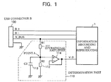
- Fig. 1 is a block diagram illustrating one example of the construction of an information recording and reproducing device according to a first embodiment of the present invention.
- this information recording and reproducing device comprises a USB connector B 100, a determination part 110 and an information recording and reproducing part 1.
- the determination part 110 includes a resistor 111 with a resistance value of R1, a resistor 112 with a resistance value of R2, a capacitor 113 with a capacitance value of C2, and an operational amplifier 114.
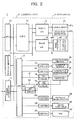
- FIG. 2 is a block diagram that illustrates one example of the construction of the information recording and reproducing part. As shown in Fig. 2, this information recording and reproducing part 1 includes a control unit 2 and an enclosure 3.
- the control unit 2 includes an upper interface 11, a buffer memory 12, an MPU ( microprocessor unit) 13, a ODC ( optical disc controller ) 14, a write LSI 15, a read LSI 16, a DSP ( digital signal processor ) 17, and an FES ( focus error signal ) detection circuit 18, a TES ( tracking error signal ) detection circuit 19, a TZC ( track zero crossing signal ) detection circuit 20, and drivers 21 - 25.
- the upper interface 11, the buffer memory 12, the MPU 13, the ODC 14, the write LSI 15, the read LSI 16 and the DSP 17 are connected with one another through a bus.
- the MPU 13, the ODC 14 and the DSP 17 together constitute a control part of this device.
- the enclosure 3 includes a laser diode unit 31, an ID and MO detector 32, a head amplifier 33, a temperature sensor 34, a spindle motor 35, and a magnetic field application part 36, a multisegment detector 37, a focus and track actuator 38, a lens actuator 39, and a VCM ( voice coil motor ) 40.
- the laser diode unit 31 has a laser diode 31 a and a monitor detector 31 b built therein.
- the upper interface 11 exchanges commands and data with an upper device connected thereto, and the buffer memory 12 is shared by the upper interface 11, the MPU 13 and the ODC 14, and it is used as a working storage or memory area.
- the MPU 13 performs the overall control of the information recording and reproducing part 1, and switches the power consumption and the operation mode based on an output of the determination part 110.
- the ODC 14 performs necessary processing to read and write data with respect to an optical disc medium.
- the write LSI 15 incorporates therein a write modulation circuit and a laser diode control circuit, and serves to convert writing data from the ODC 14 into PPM ( Pulse Phase Modulation ) recorded data or PWM ( Pulse Width Modulation ) recorded data in accordance with the type of the recording medium thereby to supply the thus converted data to the laser diode unit 31.
- the laser diode 31 a emits light based on the data from the write LSI 15, and the monitor detector 31 b detects the amount of light emitted from the laser diode 31 a and supplies the result to the write LSI 15.
- the signal detected by the ID and MO detector 32 is amplified by the head amplifier 33, and output to the read LSI 16.
- the read LSI 16 has a read demodulator circuit and a frequency synthesizer built therein, creates a read clock and read data from the output ( MO, ID ) of the head amplifier 33, and demodulates the data into the original data.
- the FES detection circuit 18 detects a focus error signal ( E1 ) based on a detection signal from the multisegment detector 37.
- the TES detection circuit 19 detects a tracking error signal ( E2 ) based on the detection signal of the multisegment detector 37.
- the TZC detection circuit 20 detects a track zero crossing signal ( E3 ) based on the tracking error signal of TES detection circuit 19.
- the DSP 17 performs a variety of kinds of servo control based on the focus error signal, the tracking error signal, the track zero crossing signal, and a temperature detection signal from the temperature sensor 34.
- the driver 21 drives the spindle motor 35 in accordance with a drive signal from the DSP 17, and the driver 22 drives the magnetic field application part 36 in accordance with a magnetic field generation signal from the DSP 17.
- the magnetic field application part 36 is comprised of an electromagnet, and is constructed so as to change the magnetic field applied to the MO recording medium in accordance with a drive signal from the driver 22.
- the magnetic field application part 36 may be of a floating type in which it floats above the recording medium under the action of a magnetic head formed of a magnetic pole and a coil wound therearound, or of a contact type in which it is in contact with the recording medium.
- the driver 23 drives the focus and track actuator 38 in accordance with a focus control signal from the DSP 17.
- the driver 24 drives the lens actuator 39 in accordance with a tracking control signal from the DSP 17.
- the driver 25 drives the VCM 40 in accordance with a VCM control signal from the DSP 17.
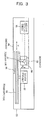
- Fig. 3 is a block diagram that illustrates one example of the schematic internal construction of the enclosure.
- this enclosure 3 comprises the spindle motor 35, the magnetic field application part 36, an MO medium 51, an MO cartridge 52, an insertion opening 53, a housing 54, a carriage 55, a prism 56, an object lens 57, and a fixed optical system 58.
- the operation inside the enclosure 3 will next be described.
- the MO cartridge 52 receiving therein the MO medium 51 is fitted into the housing 54 from the insertion opening 53, and the MO medium 51 is coupled to the spindle motor 35.
- a shutter of the MO cartridge 52 is opened so that the MO medium 51 is exposed from the MO cartridge 52, and held between the carriage 55 and the magnetic field application part 36 in the housing 54.
- the carriage 55 is arranged so as to be movable in a radial direction (direction of arrow A) of the MO medium 51 by means of the VCM 40.
- the prism 56 and the object lens 57 are installed onto the carriage 55 in a manner such that the prism 56 refracts a laser beam from the fixed optical system 58 in a direction to the MO medium 51, and the object lens 57 converges the laser beam from the prism 56 onto the MO medium 51.
- the object lens 57 is caused to swing in a direction of arrow B by means of the focus and track actuator 38 mounted on the carriage 55, as well as in the direction of arrow A by means of the lens actuator 39 mounted on the carriage 55. Focus control is carried out by the swinging motion of the object lens 57 in the direction of arrow B caused by the focus actuator 38, and tracking control is also carried out by the swinging motion of the object lens 57 in the direction of arrow B caused by the lens actuator 39.
- tracking is controlled by the VCM 40 and the lens actuator 39
- tracking control can be performed only by the use of the VCM 40 without having the cooperation of the lens actuator 39.
- the above is the operation inside the enclosure 3.
- the V_BUS is supplied to each block in the information recording and reproducing part 1, which is connected to ground, and the data is input to the upper interface 11 of the information recording and reproducing part 1.
- the V_BUS is voltage divided by the resistor 111 and the resistor 112, and a resultant voltage VA obtained at point A is input to the operational amplifier 114.
- the capacitor 113 serves to remove a high-frequency component in a variation of the V_BUS so as to prevent an overdetection of the operational amplifier 114.
- the operational amplifier 114 amplifies the voltage at point A and outputs the result to the information recording and reproducing part 1 of as a V_D.
- the V_D is input to an ADC ( analog to digital converter ) in the MPU 13, which can read the actual voltage of the V_BUS based on the value of the ADC and switch the power consumption and the operation mode in accordance with the value of the V_BUS thus read.
- ADC analog to digital converter
- M represents the state of power consumption
- the MPU 13 determines whether the V_BUS exceeds a predetermined threshold potential V_TH ( S11 ), and when the V_BUS exceeds V_TH ( S11, Yes ), the MPU 13 controls such that M becomes 0 ( S12 ).
- the MPU 13 determines whether M is equal to 2 ( S13 ), and when M is not equal to 2 ( S13, No ), the MPU 13 controls to make all the LSIs into enable states, sets the clock to the highest frequency ( S14 ), and determines whether the V_BUS exceeds V_TH (S15).
- the MPU 13 supplies a certain predetermined amount of current ( 1 ) to the focus and track actuator 38 and the like ( S16 ), and determines whether the V_BUS exceeds V_TH (S17).
- the MPU 13 supplies an amount of current ( 2 ) larger than the amount of current (1) to the focus and track actuator 38 and the like ( S18 ), and determines whether the V_BUS exceeds V_TH ( S19 ).
- the MPU 13 supplies the predetermined amount of current ( 1 ) to the focus and track actuator 38 and the like, also supplies a current the magnetic field application part 36 so as to generate a magnetic field required for erasure and writing (S20), and determines whether the V_BUS exceeds V_TH ( S21 ).
- the MPU 13 supplies the amount of current ( 2 ) to the focus and track actuator 38 and the like, also supplies a current to the magnetic field application part 36 so as to generate a magnetic field required for erasure and writing ( S22 ), and determines whether the V_BUS exceeds V_TH (S23).
- the MPU 13 switches the entire function of the information recording and reproducing device to a normal operation mode ( S24 ), and this control flow is ended in an abnormal termination, whereas when the V_BUS is below V_TH ( S23, No ), the MPU 13 inhibits supplying the current to the magnetic field application part at the same time as a seek operation, and switches the operation mode of the device into a bias first application inhibition operation mode in which current is supplied to the magnetic field application part after the seek operation has been completed ( S28 ), and this control flow is ended.
- the MPU 13 switches the operation mode of the device into a load error during a load sequence after a medium has been inserted ( S29 ), and then this control flow is ended.
- the MPU 13 adds 1 to M and shifts the control flow to processing in step S13 ( S25 ). That is, the power consumption is switched from the normal state into the power saving state, and determines again in the processing of steps S15, S17, S19 and S21 whether the V_BUS exceeds V_TH.
- the MPU 13 determines whether M is equal to 1, ( S26, No ), and if M is not equal to 1 ( S26 ), 1 is added to M ( S25 ) and the control flow shifts to the processing in step S13.
- the MPU 13 adds 1 to M ( S25 ) and shifts to the processing of step S13. That is, in the processing of step S13, M becomes equal to 2 ( S13, Yes ), and the MPU 13 switches the operation mode of the device into a load error in a load sequence after insertion of the medium ( S29 ), and this control flow is ended.
- the MPU 13 determines whether M is equal to 1 ( S26 ), and it is determined that M is equal to 1 ( S26, Yes ), so the MPU 13 switches the operation mode into a read-only operation mode that inhibits the erasure and writing of information data in the information recording and reproducing device and limits its function only to the writing of information data ( S27 ), and this control flow is ended.
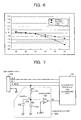
- Fig. 6 illustrates a graphical example of the result of a power supply check.
- the axis of ordinate represents the V_BUS
- the axis of abscissa represents each of states ( a ) - ( f ) in Fig. 5. Since the V_BUS is below V_TH in the state ( f ) under a first connection environment ( 1 ), the MPU 13 controls the information recording and reproducing part 1 so as to make it operate in the bias first application inhibition operation mode. On the other hand, the V_BUS exceeds V_TH in the respective states under a second connection environment ( 2 ), so the MPU 13 controls the information recording and reproducing part 1 so as to make it operate in the normal operation mode.
- the MPU 13 reads the V_BUS in each state while increasing the load current, and switches the power consumption and the operation mode in accordance with the result of the comparison between the V_BUS and V_TH.
- the MPU 13 controls the information recording and reproducing part 1 so as to make it operate with an amount of power consumption and in the operation mode thus switched.
- This embodiment illustrates another example of the determination part which, upon connection of an information recording and reproducing device, the voltage of a power supply is read while increasing a load current in its operating state, so that the power consumption and the operation mode thereof are switched in accordance with the result thus read, as in the case the first embodiment.
- Fig. 7 is a block diagram illustrating one example of the construction of the information recording and reproducing device according to the second embodiment of the present invention.
- this information recording and reproducing device comprises a USB connector B 100, a determination part 120 and an information recording and reproducing part 1A.
- the determination part 120 includes a resistor 121 with a resistance value of R1, a resistor 122 with a resistance value of R2, a capacitor 123 with a capacitance value of C2, and a comparator 124.
- the information recording and reproducing part 1A is of a construction similar to that of the information recording and reproducing part 1, but with a different input to an MPU 13.
- the same symbols as those in Fig. 1 designate the same or corresponding parts shown in Fig. 1, and an explanation thereof is omitted here.
- a reference voltage V_REF is generated from a V_BUS by using an unillustrated regulator IC or the like.
- the reference voltage V_REF thus generated is input to a non-inverting terminal of the comparator 124.
- the V_BUS is voltage divided by the resistor 121 and the resistor 122 as in the first embodiment, and a resultant voltage VA at point A thus obtained is input to an inverting terminal of the comparator 124.
- the capacitor 123 serves to remove a high-frequency component in a variation of the V_BUS so as to prevent an overdetection of the comparator 124.
- the comparator 124 makes a comparison between VA and V_REF, and outputs 0, if VA > V_REF, and 1, if VA ⁇ V_REF, to the information recording and reproducing part 1A as an ALARM ( alarm: AL ).
- the ALARM ( AL ) is input to the MPU 13 of the information recording and reproducing part 1A.
- the MPU 13 makes a comparison between the V_BUS and V_TH in Fig. 5 by the use of the ALARM, and as shown in Fig. 5, the ALARM in each state is read while increasing the load current, whereby the power supply state is ascertained so as to switch the power consumption and the operation mode in accordance with the power supply state, as in the first embodiment.
- the MPU 13 controls the information recording and reproducing part 1 so as to make it operate with an amount of power consumption and in the operation mode thus switched.
- Fig. 8 is a block diagram illustrating one example of the construction of an information recording and reproducing device according to a third embodiment of the present invention. As shown in Fig. 8, this information recording and reproducing device comprises a USB connector B 100, a determination part 130 and an information recording and reproducing part 1 B.
- the determination part 130 includes a resistor 131 with a resistance value of R1, a resistor 132 with a resistance value of R2, a capacitor 133 with a capacitance value of C2, a comparator 134, a resistor 135 with a resistance value of R3, a resistor 136 with a resistance value of R4, and a latch circuit 137.
- the information recording and reproducing part 1 B is of a construction similar to that of the information recording and reproducing part 1, but with a different input to an MPU 13. Note that in Fig. 8, the same symbols as those in Fig. 1 designate the same or corresponding parts shown in Fig. 1, and an explanation thereof is omitted here.
- a reference voltage V_REF is generated from a V_BUS, as in the second embodiment.
- a portion between the reference voltage V_REF thus generated and an output of the comparator 134 is voltage divided by the resistor 135 and the resistor 136, and a resultant voltage VB at point B thus obtained is input to a non-inverting terminal of the comparator 134.
- the V_BUS is voltage divided by the resistor 131 and the resistor 132, and a resultant voltage VA at point A thus obtained is input to the comparator 134.
- the capacitor 133 serves to remove a high-frequency component in a variation of the V_BUS so as to prevent an overdetection of the comparator 134.
- the comparator 134 makes a comparison between VA and VB, and outputs 0, if VA > VB, and 1, if VA ⁇ VB, to the information recording and reproducing part 1 B and the latch circuit 137 as an ALARM ( AL ).
- ALARM AL
- the ALARM in the form of the output of the comparator 134 has hysteresis with respect to the VA in the form of the input thereof.
- the MPU 13 does not accept an interrupt due to an ALARM in the load sequence for example, so the latch circuit 137 serves to hold an ALARM that has been generated during the time when the MPU 13 does not accept any interrupt, and output the ALARM thus held to the MPU 13 as an ALARM_LATCH ( AL - L) as necessary.
- the ALARM thus output is input to an interrupt port of the MPU 13.
- VA becomes greater than VB ( VA > VB )
- the MPU 13 checks the value of the ALARM_LATCH ( AL - L ) and switches the operation mode in accordance with the value thus checked.
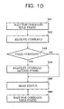
- the MPU 13 is standby or waiting for a command ( S41 ), and upon receipt of a command ( S42 ), makes a determination as to whether the command thus received is a valid command ( S43 ).
- the MPU 13 sends a status indicative of the invalid command ( S45 ), and waits again for another command ( S46 ), whereas when the received command is a valid command ( S43, Yes ), the MPU 13 executes the command ( S44 ), sends a status indicative of the completion of the command ( S45 ), and waits again for a new command.
- the MPU 13 is in an idle state in the processing of step S41 and in the processing of step S46, and the MPU 13 is in an access state in the processing of steps S42 through step S45.
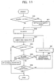
- ALARM_LATCH 0 ( S51, No )
- the control flow shifts to the processing of step S52
- ALARM_LATCH 1 (S51, Yes )
- the power consumption is switched according to the flow of Fig.
- the ALARM_LATCH is cleared ( S57 ), after which the counter is set to zero ( S52 ) and a command is executed ( S53 ). After the execution of the command, the MPU 13 makes a determination as to whether the counter exceeds a specified value N ( S54 ), and when the counter exceeds the specified value N ( S54, Yes ), abnormal status data is set ( S62 ) and this control flow is ended.
- the MPU 13 turns off the current to the magnetic field application part 36 at once, also turns off the servo such as the focus and track actuator 38 and the like, decreases the amount of light emitted by the laser diode 31 a to an amount of light corresponding to the read power, interrupts the command execution processing ( S60 ), adds 1 to the counter ( S61 ), and returns to the processing of step S53.
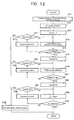
- the MPU 13 turns off the current to the magnetic field application part 36, also turns off the servo such as the focus and track actuator 38 and the like, decreases the amount of light emission of the laser diode 31a to an amount of light corresponding to the read power ( S71 ), and also lowers the system clock of each macro built into the MPU 13 ( S72 ).
- the MPU 13 first adjusts the counter to 0 ( S73 ), then decreases the number of revolutions per minute of the spindle motor 35 ( S74 ), and determines whether the number of revolutions per minute of the spindle motor 35 has become a predetermined number of revolutions per minute ( S75 ).
- the MPU 13 adds 1 to the counter ( S76 ), and determines whether the counter exceeds a specified value N ( S77 ).
- step S74 When the counter does not exceed the specified value N ( S77, No ), a return to the processing of step S74 is carried out, whereas when the counter exceeds the specified value N ( S77, Yes ), malfunction or abnormal status data is set ( S88 ), and this control flow is ended.
- the MPU 13 first adjusts the counter to 0 ( S78 ), then turns off the servo ( S79 ), and determines whether the servo has become an on state ( S80 ).
- the MPU 13 adds 1 to the counter ( S81 ), and determines whether the counter exceeds the specified value N ( S82 ).
- the MPU 13 first adjusts the counter to 0 ( S83 ), then reads ID ( S84 ), and determines whether ID has been able to be read ( S85 ).
- ID has been able to be read S85, Yes
- this control flow is ended, whereas when ID has not been able to be read ( S85, No ), the MPU 13 adds 1 to the counter ( S86 ), and determines whether the counter exceeds the specified value N ( S87 ).
- step S84 When the counter does not exceed the specified value N ( S87, No ), a return to the processing of step S84 is carried out, whereas when the counter exceeds the specified value N ( S87, Yes ), malfunction or abnormal status data is set ( S88 ), and this control flow is ended.
- an operation mode is provided in which an access time is decreased by limiting an acceleration current supplied to the focus and track actuator 38 or stopping the current supplied to the magnetic field application part 36 during seek operation, and the operation of the device can be switched into this operation mode.
- the power consumption can be limited by switching an upper limit of the PWM duty ratio.
- the MPU 13 monitors the power supply voltage during operation, and switches the power consumption and the operation mode in accordance with the result of monitoring. Further, the MPU 13 controls the information recording and reproducing part 1 so as to make it operate with an amount of power consumption and in the operation mode thus switched.
- This embodiment illustrates another example of the processing executed in case where an ALARM is generated in the processing of step S44 during the command execution in Fig. 10.
- step S55 When an ALARM is generated in the processing of step S55 ( S55, Yes ), the MPU 13 activates a timer ( S58 ), and determines whether the ALARM has been released before the timer reaches a preset specified time ( S59 ).
- the control processing shifts to step S56, whereas when an ALARM has not been released ( S59, No ), the MPU 13 turns off the current to the magnetic field application part 36, also turns off the servo such as the focus and track actuator 38 and the like, decreases the amount of light emitted by the laser diode 31 a to an amount of light corresponding to the read power, interrupts the command execution processing ( S60 ), adds 1 to the counter ( S61 ), and returns to the processing of step S53.
- the MPU 13 by monitoring whether the ALARM has been released before the timer reaches the preset specified time, the MPU 13 switches the power consumption when the ALARM has not been released even if the preset specified time is exceeded. In addition, the MPU 13 controls the information recording and reproducing part 1 so as to make it operate with an amount of power consumption thus switched.
- Fig. 14 is a block diagram that illustrates one example of the construction of an information recording and reproducing device according to a fifth embodiment of the present invention. As shown in Fig. 14, this information recording and reproducing device comprises a USB connector B 100, a determination part 140 and an information recording and reproducing part 1C.
- the determination part 140 includes a sense resistor 141 with a resistance value of RS, a resistor 142 with a resistance value of R5, a resistor 142 with a resistance value of R6, a capacitor 151 with a capacitance value of C2, an operational amplifier 144, a resistor 145 with a resistance value of R5, a resistor 146 with a resistance value of R6, a comparator 147, a resistor 148 with a resistance value of R3, a resistor 149 with a resistance value of R4, and a latch circuit 150.
- the information recording and reproducing part 1C has the same construction as that of the information recording and reproducing part 1, but is different therefrom in an input to the MPU 13. Note that in Fig. 14, the same symbols as those in Fig. 1 designate the same or corresponding parts shown in Fig. 1, and an explanation thereof is omitted here.
- the sense resistor 141 is inserted in series in a V_BUS line in the determination part 140.
- a voltage V1 and a voltage V2 are input to the determination part 140, and the voltage V2, being lowered by the sense resistor 141, is supplied to the information recording and reproducing part 1.
- a reference voltage V_REF is generated from the V_BUS, as in the second embodiment.
- a portion between the reference voltage V_REF thus generated and an output of the comparator 147 is voltage divided by the resistor 148 and the resistor 149, and a resultant voltage VB at point B thus obtained is input to a non-inverting terminal of the comparator 147.
- a voltage VC at point C which is a potential difference ( V1 - V2 ) across the opposite ends of the sense resistor 141 amplified by the operational amplifier 144, is input to an inverting terminal of the comparator 147.
- the capacitor 151 serves to remove a high-frequency component in a current variation so as to prevent an overdetection of the comparator 147.
- the comparator 147 makes a comparison between VC and VB, and outputs 0, if VC > VB, and 1, if VC ⁇ VB, to the information recording and reproducing part 1C and the latch circuit 150 as an ALARM' ( AL' ).
- AL' ALARM'
- the ALARM' in the form of the output of the comparator 147 has hysteresis with respect to the VC in the form of the input thereof.
- the latch circuit 150 holds the ALARM' generated during the time when the MPU 13 does not accept any interrupt, and outputs the ALARM' thus held to the MPU 13 as an ALARM_LATCH' ( AL - L' ) as necessary.
- the ALARM' and ALARM_LATCH' are input to an interrupt port of the MPU 13, and are inverted there into an ALARM and an ALARM_LATCH, respectively.
- the MPU 13 controls the power consumption in the normal state.
- the MPU 13 switches the power consumption and the operation mode in accordance with the operating state.
- the switching of the power consumption and the operation mode during the load sequence, the command standby or waiting time, and the command execution time is similar to that in the third embodiment.
- the MPU 13 monitors the power supply voltage during operation, and switches the power consumption and the operation mode in accordance with the result of monitoring. In addition, the MPU 13 controls the information recording and reproducing part 1 so as to make it operate with an amount of power consumption and in the operation mode thus switched.
- the present invention can be applied to the case where power is supplied, for example, from a battery such as a dry battery or cell, etc.
- the constructions and operations of the information recording and reproducing devices described in the above-mentioned first through fifth embodiments are examples for achieving the present invention, but it is needless to say that their constructions are not particularly limited in any manner but can be applied in an appropriate manner within the scope of the present invention not departing from the spirit thereof.
- the invention can be applied to devices which are used only for the purpose of reproduction or recording.
- the power supply voltage or the power supply current which can be varied in accordance with the use environment of the information storage device, is monitored so that the power consumption of the device can be suppressed or the function thereof can be limited in accordance with the value of the power supply voltage or the power supply current, whereby the device can continue stable operation, thus making it possible to eliminate trouble such as a crash of the information storage device during operation.
Landscapes
- Engineering & Computer Science (AREA)
- Theoretical Computer Science (AREA)
- Physics & Mathematics (AREA)
- General Engineering & Computer Science (AREA)
- General Physics & Mathematics (AREA)
- Power Sources (AREA)
Abstract
Description
Subsequently, a power supply check is performed ( S4 ), and a load sequence is carried out ( S5 ).
Claims (17)
- An information storage device adapted to use a power supply supplied from an interface or a battery, said device comprising:a first electrical parameter monitoring part that monitors an electrical parameter in respect of the power input from said power supply;a determination part that determines, based on the result of monitoring the electrical parameter by said first electrical parameter monitoring part, whether control is to be performed by limiting the operation or function of said device at the start of supplying power from said power supply; anda first control part that operates said device by limiting the operation or function thereof based on the determination of said determination part.
- The information storage device as set forth in claim 1, characterized in that said first control part limits, based on said monitoring result, the operation or function of said device to an operational or functional range which the capacity of said power supply at the start of supplying power from said power supply is able to permit.
- The information storage device as set forth in claim 1, characterized in that said first electrical parameter monitoring part includes a power consumption increasing part that increases the power consumption of said device in a stepwise manner, and monitors said electrical parameter in each step in which the power consumption is increased stepwise.
- The information storage device as set forth in claim 1, characterized by comprising:wherein said first control part selects one operation mode from the plurality of operation modes set by said operation mode setting part based on the monitoring result of said first electrical parameter monitoring part.an operation mode setting part that sets a plurality of operation modes corresponding to the magnitude of said electrical parameter in a selectable manner;
- The information storage device as set forth in claim 1, characterized in that said operation mode includes at least one of a read-only operation mode, a normal operation mode, and a bias first application inhibition operation mode.
- The information storage device as set forth in claim 1, characterized in that said electrical parameter is a voltage value or a current value.
- An information storage device adapted to use a power supply supplied from an interface or a battery, said device comprising:a second electrical parameter monitoring part that monitors an electrical parameter in respect of the power input from said power supply during operation in which power is being supplied; anda second control part that limits the operation or function of said device to an operational or functional range which said power supply is able to permit, by reducing the power consumption of said device based on the result of monitoring said electrical parameter by said second electrical parameter monitoring part.
- The information storage device as set forth in claim 7, characterized in that said second control part limits the number of revolutions per minute of a spindle motor.
- The information storage device as set forth in claim 7, characterized in that said second control part limits an access time.
- The information storage device as set forth in claim 7, characterized in that said second control part limits the frequency of a system clock.
- The information storage device as set forth in claim 7, characterized in that in the case of an actuator being driven by using PWM, said second control part limits the duty ratio of said PWM.
- The information storage device as set forth in claim 7, characterized in that the monitoring result of said second electrical parameter monitoring part is the result of monitoring a change in the magnitude of said electrical parameter over a predetermined period of time.
- The information storage device as set forth in claim 12, characterized in that said second electrical parameter monitoring part performs monitoring by providing hysteresis to said electrical parameter.
- The information storage device as set forth in claim 7, characterized in that when said electrical parameter falls below a predetermined value, said second electrical parameter monitoring part generates an alarm, which is held until an interrupt becomes possible.
- The information storage device as set forth in claim 14, characterized in that when said alarm is generated in a load sequence, said second control part limits the function of said device thereafter only to reading information.
- The information storage device as set forth in claim 14, characterized in that said second control part limits the power consumption of said device when said alarm is generated during a command standby or command execution time.
- The information storage device as set forth in claim 14, characterized in that said second control part limits the power consumption of said device in case where said alarm is generated during a command standby or command execution time, and is not released even if a predetermined period of time has elapsed.
Priority Applications (1)
| Application Number | Priority Date | Filing Date | Title |
|---|---|---|---|
| EP07115117A EP1863029A1 (en) | 2002-06-28 | 2002-06-28 | Information storage device |
Applications Claiming Priority (1)
| Application Number | Priority Date | Filing Date | Title |
|---|---|---|---|
| PCT/JP2002/006573 WO2004003913A1 (en) | 2002-06-28 | 2002-06-28 | Information storage device |
Related Child Applications (1)
| Application Number | Title | Priority Date | Filing Date |
|---|---|---|---|
| EP07115117A Division EP1863029A1 (en) | 2002-06-28 | 2002-06-28 | Information storage device |
Publications (2)
| Publication Number | Publication Date |
|---|---|
| EP1533814A1 true EP1533814A1 (en) | 2005-05-25 |
| EP1533814A4 EP1533814A4 (en) | 2006-11-22 |
Family
ID=29808165
Family Applications (2)
| Application Number | Title | Priority Date | Filing Date |
|---|---|---|---|
| EP02738863A Withdrawn EP1533814A4 (en) | 2002-06-28 | 2002-06-28 | INFORMATION STORAGE DEVICE |
| EP07115117A Withdrawn EP1863029A1 (en) | 2002-06-28 | 2002-06-28 | Information storage device |
Family Applications After (1)
| Application Number | Title | Priority Date | Filing Date |
|---|---|---|---|
| EP07115117A Withdrawn EP1863029A1 (en) | 2002-06-28 | 2002-06-28 | Information storage device |
Country Status (6)
| Country | Link |
|---|---|
| US (1) | US7373529B2 (en) |
| EP (2) | EP1533814A4 (en) |
| JP (1) | JPWO2004003913A1 (en) |
| CN (1) | CN1628354A (en) |
| AU (1) | AU2002313299A1 (en) |
| WO (1) | WO2004003913A1 (en) |
Families Citing this family (9)
| Publication number | Priority date | Publication date | Assignee | Title |
|---|---|---|---|---|
| JP4710335B2 (en) * | 2005-02-01 | 2011-06-29 | パナソニック株式会社 | Power supply diagnosis method for disk device |
| JP2006262610A (en) * | 2005-03-16 | 2006-09-28 | Mitsumi Electric Co Ltd | Power circuit |
| US7698490B2 (en) * | 2005-12-21 | 2010-04-13 | Nvidia Corporation | Passive USB power configuration switching |
| US8604709B2 (en) | 2007-07-31 | 2013-12-10 | Lsi Industries, Inc. | Methods and systems for controlling electrical power to DC loads |
| US8903577B2 (en) | 2009-10-30 | 2014-12-02 | Lsi Industries, Inc. | Traction system for electrically powered vehicles |
| US7598683B1 (en) | 2007-07-31 | 2009-10-06 | Lsi Industries, Inc. | Control of light intensity using pulses of a fixed duration and frequency |
| KR101723389B1 (en) * | 2011-01-10 | 2017-04-18 | 삼성전자주식회사 | Method and apparatus for adaptive operation of application |
| US9395799B2 (en) | 2012-08-09 | 2016-07-19 | Nvidia Corporation | Power management techniques for USB interfaces |
| US11233679B2 (en) * | 2020-06-01 | 2022-01-25 | Hewlett Packard Enterprise Development Lp | Phase adjustments for computer nodes |
Family Cites Families (24)
| Publication number | Priority date | Publication date | Assignee | Title |
|---|---|---|---|---|
| JPS53138246A (en) | 1977-05-10 | 1978-12-02 | Toshiba Corp | Initial program load control system |
| JPS5841455A (en) | 1981-09-01 | 1983-03-10 | Toshiba Corp | Power supply circuit for stabilizing automatic stop device operation |
| JPS6217842A (en) | 1985-07-16 | 1987-01-26 | Hitachi Ltd | Program management method |
| JPS62155721A (en) | 1985-12-27 | 1987-07-10 | 日新電機株式会社 | Source cut-off detection |
| GB8801067D0 (en) | 1988-01-19 | 1988-02-17 | Exxon Chemical Patents Inc | Zeolite l preparation |
| JP2632963B2 (en) | 1988-09-19 | 1997-07-23 | キヤノン株式会社 | Recording or playback device |
| JP2791061B2 (en) * | 1988-10-28 | 1998-08-27 | オリンパス光学工業株式会社 | Power supply voltage display |
| JPH03229332A (en) | 1990-02-05 | 1991-10-11 | Toshiba Corp | Microcomputer system |
| JP3096489B2 (en) * | 1991-07-09 | 2000-10-10 | 富士通株式会社 | Disk unit |
| JPH08335357A (en) | 1995-06-08 | 1996-12-17 | Fujitsu Ltd | Storage device |
| JP3387709B2 (en) * | 1995-10-31 | 2003-03-17 | ミネベア株式会社 | Information recording device |
| US5838515A (en) * | 1996-04-30 | 1998-11-17 | Quantum Corporation | PWM/linear driver for disk drive voice coil actuator |
| JPH09306084A (en) * | 1996-05-15 | 1997-11-28 | Sharp Corp | Optical disk recording and playback device |
| JPH10162483A (en) * | 1996-11-29 | 1998-06-19 | Sony Corp | Recording / reproducing method and recording / reproducing apparatus |
| JP3069308B2 (en) | 1997-05-13 | 2000-07-24 | 日本軽金属株式会社 | Attenuator for illuminance adjustment |
| JP3627458B2 (en) | 1997-07-30 | 2005-03-09 | ミツミ電機株式会社 | Drive output monitoring circuit |
| JP3926031B2 (en) | 1998-04-15 | 2007-06-06 | ティアック株式会社 | Disk unit |
| JP2000267681A (en) * | 1999-03-16 | 2000-09-29 | Aiwa Co Ltd | Voice output device |
| JP3792066B2 (en) | 1999-03-31 | 2006-06-28 | シャープ株式会社 | Low power consumption peripherals |
| JP2000353032A (en) | 1999-06-10 | 2000-12-19 | Seiko Epson Corp | Peripheral devices with power saving function |
| JP2001067156A (en) | 1999-08-27 | 2001-03-16 | Canon Inc | Computer peripheral device, control method therefor, imaging apparatus, and storage medium |
| JP4547771B2 (en) * | 2000-04-28 | 2010-09-22 | ソニー株式会社 | Information processing system, information processing method, and information processing apparatus |
| JP4516664B2 (en) * | 2000-05-11 | 2010-08-04 | 株式会社ケンウッド | Oscillator power supply voltage drop compensation circuit |
| JP2002117616A (en) * | 2001-08-22 | 2002-04-19 | Hitachi Ltd | Disk device |
-
2002
- 2002-06-28 AU AU2002313299A patent/AU2002313299A1/en not_active Abandoned
- 2002-06-28 WO PCT/JP2002/006573 patent/WO2004003913A1/en not_active Ceased
- 2002-06-28 JP JP2004517215A patent/JPWO2004003913A1/en active Pending
- 2002-06-28 EP EP02738863A patent/EP1533814A4/en not_active Withdrawn
- 2002-06-28 EP EP07115117A patent/EP1863029A1/en not_active Withdrawn
- 2002-06-28 CN CN02829038.0A patent/CN1628354A/en active Pending
-
2004
- 2004-12-08 US US11/007,460 patent/US7373529B2/en not_active Expired - Fee Related
Also Published As
| Publication number | Publication date |
|---|---|
| WO2004003913A1 (en) | 2004-01-08 |
| EP1533814A4 (en) | 2006-11-22 |
| US7373529B2 (en) | 2008-05-13 |
| JPWO2004003913A1 (en) | 2005-11-04 |
| CN1628354A (en) | 2005-06-15 |
| US20050102542A1 (en) | 2005-05-12 |
| AU2002313299A1 (en) | 2004-01-19 |
| EP1863029A1 (en) | 2007-12-05 |
Similar Documents
| Publication | Publication Date | Title |
|---|---|---|
| KR100424484B1 (en) | A power supply for central processing unit | |
| EP0522483B1 (en) | Computer apparatus and storage device having controlled power saving apparatus | |
| US6510400B1 (en) | Temperature control circuit for central processing unit | |
| US6295569B1 (en) | Storage apparatus | |
| US8286018B2 (en) | Power management in data storage device determining utilization of a control circuit by its rate of command processing | |
| EP1533814A1 (en) | Information storage device | |
| US6625739B1 (en) | Hard power shutdown of a computer by actuating both a keyboard controller independent key and a soft power switch together to bypass the power switch together to bypass the power controller | |
| KR20030081001A (en) | Multi-voltage power-up stable input/output buffer circuit in a disc drive | |
| US6011667A (en) | Disk drive system configurable for multiple supply voltages | |
| JP3961142B2 (en) | Disk drive control method and control apparatus | |
| WO2004109676A1 (en) | Information recording/reproduction device and method | |
| JP2576740B2 (en) | Disk unit | |
| JP3926031B2 (en) | Disk unit | |
| US7092190B2 (en) | Dynamic power supply | |
| US20070150765A1 (en) | Information processing apparatus having electronic device whose operating speed is controlled, and method of controlling the operating speed of the electronic device | |
| JP3487341B2 (en) | Data converter | |
| US8982497B2 (en) | Class-AB amplifier, motor drive device, magnetic disk storage device, and electronic apparatus | |
| JPWO2003009559A1 (en) | Peripheral equipment | |
| JP4273872B2 (en) | Optical disk device and disk device | |
| JP2006309912A (en) | Optical disc apparatus and recording / reproducing method of optical disc apparatus | |
| CN216979719U (en) | USB power supply switching circuit and USB power supply device | |
| JP2004152344A (en) | Removable disk drive | |
| JP2830623B2 (en) | Drive control IC device for small hard disk drive | |
| JP2005346870A (en) | Information recording / reproducing device with power supply voltage monitoring function | |
| JP3892007B2 (en) | Disk drive control method and control apparatus |
Legal Events
| Date | Code | Title | Description |
|---|---|---|---|
| PUAI | Public reference made under article 153(3) epc to a published international application that has entered the european phase |
Free format text: ORIGINAL CODE: 0009012 |
|
| 17P | Request for examination filed |
Effective date: 20050105 |
|
| AK | Designated contracting states |
Kind code of ref document: A1 Designated state(s): AT BE CH CY DE DK ES FI FR GB GR IE IT LI LU MC NL PT SE TR |
|
| AX | Request for extension of the european patent |
Extension state: AL LT LV MK RO SI |
|
| DAX | Request for extension of the european patent (deleted) | ||
| RBV | Designated contracting states (corrected) |
Designated state(s): DE FR GB |
|
| A4 | Supplementary search report drawn up and despatched |
Effective date: 20061023 |
|
| RIC1 | Information provided on ipc code assigned before grant |
Ipc: G11B 19/00 20060101AFI20061017BHEP |
|
| 17Q | First examination report despatched |
Effective date: 20070329 |
|
| GRAP | Despatch of communication of intention to grant a patent |
Free format text: ORIGINAL CODE: EPIDOSNIGR1 |
|
| STAA | Information on the status of an ep patent application or granted ep patent |
Free format text: STATUS: THE APPLICATION HAS BEEN WITHDRAWN |
|
| 18W | Application withdrawn |
Effective date: 20080609 |