EP1532663B1 - Three dimensional thin film device fabrication methods - Google Patents
Three dimensional thin film device fabrication methods Download PDFInfo
- Publication number
- EP1532663B1 EP1532663B1 EP03764605.6A EP03764605A EP1532663B1 EP 1532663 B1 EP1532663 B1 EP 1532663B1 EP 03764605 A EP03764605 A EP 03764605A EP 1532663 B1 EP1532663 B1 EP 1532663B1
- Authority
- EP
- European Patent Office
- Prior art keywords
- layer
- thin film
- layers
- base
- shape
- Prior art date
- Legal status (The legal status is an assumption and is not a legal conclusion. Google has not performed a legal analysis and makes no representation as to the accuracy of the status listed.)
- Expired - Lifetime
Links
- 239000010409 thin film Substances 0.000 title claims description 94
- 238000000034 method Methods 0.000 title claims description 73
- 238000004519 manufacturing process Methods 0.000 title claims description 22
- 239000000463 material Substances 0.000 claims description 52
- 239000000758 substrate Substances 0.000 claims description 24
- 238000000151 deposition Methods 0.000 claims description 15
- 229910001285 shape-memory alloy Inorganic materials 0.000 claims description 11
- 238000005530 etching Methods 0.000 claims description 9
- 230000008021 deposition Effects 0.000 claims description 6
- 238000010438 heat treatment Methods 0.000 claims description 6
- VYZAMTAEIAYCRO-UHFFFAOYSA-N Chromium Chemical compound [Cr] VYZAMTAEIAYCRO-UHFFFAOYSA-N 0.000 claims description 4
- 238000000059 patterning Methods 0.000 claims description 3
- RYGMFSIKBFXOCR-UHFFFAOYSA-N Copper Chemical compound [Cu] RYGMFSIKBFXOCR-UHFFFAOYSA-N 0.000 claims description 2
- 229910052782 aluminium Inorganic materials 0.000 claims description 2
- XAGFODPZIPBFFR-UHFFFAOYSA-N aluminium Chemical compound [Al] XAGFODPZIPBFFR-UHFFFAOYSA-N 0.000 claims description 2
- 229910052804 chromium Inorganic materials 0.000 claims description 2
- 239000011651 chromium Substances 0.000 claims description 2
- 229910052802 copper Inorganic materials 0.000 claims description 2
- 239000010949 copper Substances 0.000 claims description 2
- 239000010410 layer Substances 0.000 description 105
- 238000004544 sputter deposition Methods 0.000 description 22
- 210000004204 blood vessel Anatomy 0.000 description 20
- 206010002329 Aneurysm Diseases 0.000 description 18
- 229910010380 TiNi Inorganic materials 0.000 description 17
- 235000012431 wafers Nutrition 0.000 description 16
- 229920002120 photoresistant polymer Polymers 0.000 description 15
- 230000008569 process Effects 0.000 description 15
- 238000007493 shaping process Methods 0.000 description 14
- 238000013461 design Methods 0.000 description 12
- 229910052751 metal Inorganic materials 0.000 description 12
- XKRFYHLGVUSROY-UHFFFAOYSA-N Argon Chemical compound [Ar] XKRFYHLGVUSROY-UHFFFAOYSA-N 0.000 description 11
- 208000007536 Thrombosis Diseases 0.000 description 11
- 239000000956 alloy Substances 0.000 description 11
- 239000002184 metal Substances 0.000 description 11
- 229910001000 nickel titanium Inorganic materials 0.000 description 10
- 229910045601 alloy Inorganic materials 0.000 description 9
- 238000003780 insertion Methods 0.000 description 9
- 230000037431 insertion Effects 0.000 description 9
- 230000009466 transformation Effects 0.000 description 9
- 210000004369 blood Anatomy 0.000 description 7
- 239000008280 blood Substances 0.000 description 7
- HLXZNVUGXRDIFK-UHFFFAOYSA-N nickel titanium Chemical compound [Ti].[Ti].[Ti].[Ti].[Ti].[Ti].[Ti].[Ti].[Ti].[Ti].[Ti].[Ni].[Ni].[Ni].[Ni].[Ni].[Ni].[Ni].[Ni].[Ni].[Ni].[Ni].[Ni].[Ni].[Ni] HLXZNVUGXRDIFK-UHFFFAOYSA-N 0.000 description 7
- 238000000206 photolithography Methods 0.000 description 7
- XUIMIQQOPSSXEZ-UHFFFAOYSA-N Silicon Chemical compound [Si] XUIMIQQOPSSXEZ-UHFFFAOYSA-N 0.000 description 6
- 229910052786 argon Inorganic materials 0.000 description 6
- 239000010408 film Substances 0.000 description 6
- 239000000203 mixture Substances 0.000 description 6
- 239000010703 silicon Substances 0.000 description 6
- 229910052710 silicon Inorganic materials 0.000 description 6
- 230000007704 transition Effects 0.000 description 6
- PXHVJJICTQNCMI-UHFFFAOYSA-N Nickel Chemical compound [Ni] PXHVJJICTQNCMI-UHFFFAOYSA-N 0.000 description 4
- 230000003872 anastomosis Effects 0.000 description 4
- 238000010586 diagram Methods 0.000 description 4
- 239000000126 substance Substances 0.000 description 4
- 238000000137 annealing Methods 0.000 description 3
- 230000008901 benefit Effects 0.000 description 3
- 230000017531 blood circulation Effects 0.000 description 3
- 230000036760 body temperature Effects 0.000 description 3
- 210000004556 brain Anatomy 0.000 description 3
- 239000007789 gas Substances 0.000 description 3
- 239000011521 glass Substances 0.000 description 3
- 238000007917 intracranial administration Methods 0.000 description 3
- 238000005304 joining Methods 0.000 description 3
- 229910001092 metal group alloy Inorganic materials 0.000 description 3
- 229910052759 nickel Inorganic materials 0.000 description 3
- 239000004033 plastic Substances 0.000 description 3
- 229920003023 plastic Polymers 0.000 description 3
- 238000001552 radio frequency sputter deposition Methods 0.000 description 3
- 241000894007 species Species 0.000 description 3
- 239000013077 target material Substances 0.000 description 3
- 210000001519 tissue Anatomy 0.000 description 3
- 239000010936 titanium Substances 0.000 description 3
- 229910052719 titanium Inorganic materials 0.000 description 3
- 201000008450 Intracranial aneurysm Diseases 0.000 description 2
- XEEYBQQBJWHFJM-UHFFFAOYSA-N Iron Chemical compound [Fe] XEEYBQQBJWHFJM-UHFFFAOYSA-N 0.000 description 2
- KDLHZDBZIXYQEI-UHFFFAOYSA-N Palladium Chemical compound [Pd] KDLHZDBZIXYQEI-UHFFFAOYSA-N 0.000 description 2
- -1 argon ions Chemical class 0.000 description 2
- 230000015572 biosynthetic process Effects 0.000 description 2
- 230000008859 change Effects 0.000 description 2
- 238000011161 development Methods 0.000 description 2
- 239000003814 drug Substances 0.000 description 2
- 238000009713 electroplating Methods 0.000 description 2
- 210000001508 eye Anatomy 0.000 description 2
- 230000035876 healing Effects 0.000 description 2
- 150000002500 ions Chemical class 0.000 description 2
- 238000003698 laser cutting Methods 0.000 description 2
- 238000001459 lithography Methods 0.000 description 2
- 239000007787 solid Substances 0.000 description 2
- 239000010935 stainless steel Substances 0.000 description 2
- 229910001220 stainless steel Inorganic materials 0.000 description 2
- 229910002070 thin film alloy Inorganic materials 0.000 description 2
- 210000005166 vasculature Anatomy 0.000 description 2
- 238000003466 welding Methods 0.000 description 2
- 208000005189 Embolism Diseases 0.000 description 1
- 208000032382 Ischaemic stroke Diseases 0.000 description 1
- 229910000990 Ni alloy Inorganic materials 0.000 description 1
- 208000031481 Pathologic Constriction Diseases 0.000 description 1
- 230000018199 S phase Effects 0.000 description 1
- 208000006011 Stroke Diseases 0.000 description 1
- 208000001435 Thromboembolism Diseases 0.000 description 1
- RTAQQCXQSZGOHL-UHFFFAOYSA-N Titanium Chemical group [Ti] RTAQQCXQSZGOHL-UHFFFAOYSA-N 0.000 description 1
- HZEWFHLRYVTOIW-UHFFFAOYSA-N [Ti].[Ni] Chemical compound [Ti].[Ni] HZEWFHLRYVTOIW-UHFFFAOYSA-N 0.000 description 1
- 230000004308 accommodation Effects 0.000 description 1
- 239000000853 adhesive Substances 0.000 description 1
- 230000001070 adhesive effect Effects 0.000 description 1
- 238000005275 alloying Methods 0.000 description 1
- 238000004873 anchoring Methods 0.000 description 1
- 239000002473 artificial blood Substances 0.000 description 1
- 229910001566 austenite Inorganic materials 0.000 description 1
- 210000000601 blood cell Anatomy 0.000 description 1
- 230000036772 blood pressure Effects 0.000 description 1
- 238000005219 brazing Methods 0.000 description 1
- 210000005252 bulbus oculi Anatomy 0.000 description 1
- 210000001715 carotid artery Anatomy 0.000 description 1
- 210000004027 cell Anatomy 0.000 description 1
- 238000003486 chemical etching Methods 0.000 description 1
- 230000006835 compression Effects 0.000 description 1
- 238000007906 compression Methods 0.000 description 1
- 238000009833 condensation Methods 0.000 description 1
- 230000005494 condensation Effects 0.000 description 1
- 238000011109 contamination Methods 0.000 description 1
- 210000004087 cornea Anatomy 0.000 description 1
- 239000013078 crystal Substances 0.000 description 1
- 238000002425 crystallisation Methods 0.000 description 1
- 230000008025 crystallization Effects 0.000 description 1
- GUJOJGAPFQRJSV-UHFFFAOYSA-N dialuminum;dioxosilane;oxygen(2-);hydrate Chemical compound O.[O-2].[O-2].[O-2].[Al+3].[Al+3].O=[Si]=O.O=[Si]=O.O=[Si]=O.O=[Si]=O GUJOJGAPFQRJSV-UHFFFAOYSA-N 0.000 description 1
- 230000000694 effects Effects 0.000 description 1
- 239000005357 flat glass Substances 0.000 description 1
- 229910052735 hafnium Inorganic materials 0.000 description 1
- VBJZVLUMGGDVMO-UHFFFAOYSA-N hafnium atom Chemical compound [Hf] VBJZVLUMGGDVMO-UHFFFAOYSA-N 0.000 description 1
- 239000007943 implant Substances 0.000 description 1
- 238000002513 implantation Methods 0.000 description 1
- 239000011261 inert gas Substances 0.000 description 1
- 229910052742 iron Inorganic materials 0.000 description 1
- 239000007788 liquid Substances 0.000 description 1
- 238000011068 loading method Methods 0.000 description 1
- 238000001755 magnetron sputter deposition Methods 0.000 description 1
- 229910000734 martensite Inorganic materials 0.000 description 1
- 239000008204 material by function Substances 0.000 description 1
- 239000012528 membrane Substances 0.000 description 1
- 230000003446 memory effect Effects 0.000 description 1
- 239000007769 metal material Substances 0.000 description 1
- 150000002739 metals Chemical class 0.000 description 1
- 238000002324 minimally invasive surgery Methods 0.000 description 1
- 210000003205 muscle Anatomy 0.000 description 1
- 229910052763 palladium Inorganic materials 0.000 description 1
- 230000002093 peripheral effect Effects 0.000 description 1
- 229920000642 polymer Polymers 0.000 description 1
- 239000011241 protective layer Substances 0.000 description 1
- 238000011084 recovery Methods 0.000 description 1
- 230000004044 response Effects 0.000 description 1
- 239000012781 shape memory material Substances 0.000 description 1
- 238000005476 soldering Methods 0.000 description 1
- 239000002904 solvent Substances 0.000 description 1
- 238000004528 spin coating Methods 0.000 description 1
- 238000005477 sputtering target Methods 0.000 description 1
- 208000037804 stenosis Diseases 0.000 description 1
- 230000036262 stenosis Effects 0.000 description 1
- 239000002344 surface layer Substances 0.000 description 1
- 230000001225 therapeutic effect Effects 0.000 description 1
- 238000007736 thin film deposition technique Methods 0.000 description 1
- 229910052720 vanadium Inorganic materials 0.000 description 1
- LEONUFNNVUYDNQ-UHFFFAOYSA-N vanadium atom Chemical compound [V] LEONUFNNVUYDNQ-UHFFFAOYSA-N 0.000 description 1
- 230000002792 vascular Effects 0.000 description 1
- 208000019553 vascular disease Diseases 0.000 description 1
- 239000011800 void material Substances 0.000 description 1
- 238000001039 wet etching Methods 0.000 description 1
Images






Classifications
-
- A—HUMAN NECESSITIES
- A61—MEDICAL OR VETERINARY SCIENCE; HYGIENE
- A61B—DIAGNOSIS; SURGERY; IDENTIFICATION
- A61B17/00—Surgical instruments, devices or methods
- A61B17/12—Surgical instruments, devices or methods for ligaturing or otherwise compressing tubular parts of the body, e.g. blood vessels or umbilical cord
- A61B17/12022—Occluding by internal devices, e.g. balloons or releasable wires
-
- A—HUMAN NECESSITIES
- A61—MEDICAL OR VETERINARY SCIENCE; HYGIENE
- A61B—DIAGNOSIS; SURGERY; IDENTIFICATION
- A61B17/00—Surgical instruments, devices or methods
- A61B17/12—Surgical instruments, devices or methods for ligaturing or otherwise compressing tubular parts of the body, e.g. blood vessels or umbilical cord
-
- A—HUMAN NECESSITIES
- A61—MEDICAL OR VETERINARY SCIENCE; HYGIENE
- A61B—DIAGNOSIS; SURGERY; IDENTIFICATION
- A61B17/00—Surgical instruments, devices or methods
- A61B17/12—Surgical instruments, devices or methods for ligaturing or otherwise compressing tubular parts of the body, e.g. blood vessels or umbilical cord
- A61B17/12022—Occluding by internal devices, e.g. balloons or releasable wires
- A61B17/12099—Occluding by internal devices, e.g. balloons or releasable wires characterised by the location of the occluder
- A61B17/12109—Occluding by internal devices, e.g. balloons or releasable wires characterised by the location of the occluder in a blood vessel
- A61B17/12113—Occluding by internal devices, e.g. balloons or releasable wires characterised by the location of the occluder in a blood vessel within an aneurysm
-
- A—HUMAN NECESSITIES
- A61—MEDICAL OR VETERINARY SCIENCE; HYGIENE
- A61B—DIAGNOSIS; SURGERY; IDENTIFICATION
- A61B17/00—Surgical instruments, devices or methods
- A61B17/12—Surgical instruments, devices or methods for ligaturing or otherwise compressing tubular parts of the body, e.g. blood vessels or umbilical cord
- A61B17/12022—Occluding by internal devices, e.g. balloons or releasable wires
- A61B17/12131—Occluding by internal devices, e.g. balloons or releasable wires characterised by the type of occluding device
-
- A—HUMAN NECESSITIES
- A61—MEDICAL OR VETERINARY SCIENCE; HYGIENE
- A61B—DIAGNOSIS; SURGERY; IDENTIFICATION
- A61B17/00—Surgical instruments, devices or methods
- A61B17/12—Surgical instruments, devices or methods for ligaturing or otherwise compressing tubular parts of the body, e.g. blood vessels or umbilical cord
- A61B17/12022—Occluding by internal devices, e.g. balloons or releasable wires
- A61B17/12131—Occluding by internal devices, e.g. balloons or releasable wires characterised by the type of occluding device
- A61B17/12168—Occluding by internal devices, e.g. balloons or releasable wires characterised by the type of occluding device having a mesh structure
- A61B17/12172—Occluding by internal devices, e.g. balloons or releasable wires characterised by the type of occluding device having a mesh structure having a pre-set deployed three-dimensional shape
-
- A—HUMAN NECESSITIES
- A61—MEDICAL OR VETERINARY SCIENCE; HYGIENE
- A61B—DIAGNOSIS; SURGERY; IDENTIFICATION
- A61B17/00—Surgical instruments, devices or methods
- A61B17/22—Implements for squeezing-off ulcers or the like on inner organs of the body; Implements for scraping-out cavities of body organs, e.g. bones; for invasive removal or destruction of calculus using mechanical vibrations; for removing obstructions in blood vessels, not otherwise provided for
- A61B17/221—Gripping devices in the form of loops or baskets for gripping calculi or similar types of obstructions
-
- A—HUMAN NECESSITIES
- A61—MEDICAL OR VETERINARY SCIENCE; HYGIENE
- A61F—FILTERS IMPLANTABLE INTO BLOOD VESSELS; PROSTHESES; DEVICES PROVIDING PATENCY TO, OR PREVENTING COLLAPSING OF, TUBULAR STRUCTURES OF THE BODY, e.g. STENTS; ORTHOPAEDIC, NURSING OR CONTRACEPTIVE DEVICES; FOMENTATION; TREATMENT OR PROTECTION OF EYES OR EARS; BANDAGES, DRESSINGS OR ABSORBENT PADS; FIRST-AID KITS
- A61F2/00—Filters implantable into blood vessels; Prostheses, i.e. artificial substitutes or replacements for parts of the body; Appliances for connecting them with the body; Devices providing patency to, or preventing collapsing of, tubular structures of the body, e.g. stents
- A61F2/82—Devices providing patency to, or preventing collapsing of, tubular structures of the body, e.g. stents
- A61F2/86—Stents in a form characterised by the wire-like elements; Stents in the form characterised by a net-like or mesh-like structure
- A61F2/90—Stents in a form characterised by the wire-like elements; Stents in the form characterised by a net-like or mesh-like structure characterised by a net-like or mesh-like structure
- A61F2/91—Stents in a form characterised by the wire-like elements; Stents in the form characterised by a net-like or mesh-like structure characterised by a net-like or mesh-like structure made from perforated sheets or tubes, e.g. perforated by laser cuts or etched holes
-
- A—HUMAN NECESSITIES
- A61—MEDICAL OR VETERINARY SCIENCE; HYGIENE
- A61B—DIAGNOSIS; SURGERY; IDENTIFICATION
- A61B17/00—Surgical instruments, devices or methods
- A61B2017/00526—Methods of manufacturing
-
- A—HUMAN NECESSITIES
- A61—MEDICAL OR VETERINARY SCIENCE; HYGIENE
- A61B—DIAGNOSIS; SURGERY; IDENTIFICATION
- A61B17/00—Surgical instruments, devices or methods
- A61B2017/00831—Material properties
- A61B2017/00867—Material properties shape memory effect
-
- A—HUMAN NECESSITIES
- A61—MEDICAL OR VETERINARY SCIENCE; HYGIENE
- A61B—DIAGNOSIS; SURGERY; IDENTIFICATION
- A61B17/00—Surgical instruments, devices or methods
- A61B17/12—Surgical instruments, devices or methods for ligaturing or otherwise compressing tubular parts of the body, e.g. blood vessels or umbilical cord
- A61B17/12022—Occluding by internal devices, e.g. balloons or releasable wires
- A61B2017/1205—Introduction devices
-
- A—HUMAN NECESSITIES
- A61—MEDICAL OR VETERINARY SCIENCE; HYGIENE
- A61B—DIAGNOSIS; SURGERY; IDENTIFICATION
- A61B17/00—Surgical instruments, devices or methods
- A61B17/22—Implements for squeezing-off ulcers or the like on inner organs of the body; Implements for scraping-out cavities of body organs, e.g. bones; for invasive removal or destruction of calculus using mechanical vibrations; for removing obstructions in blood vessels, not otherwise provided for
- A61B17/221—Gripping devices in the form of loops or baskets for gripping calculi or similar types of obstructions
- A61B2017/2212—Gripping devices in the form of loops or baskets for gripping calculi or similar types of obstructions having a closed distal end, e.g. a loop
-
- A—HUMAN NECESSITIES
- A61—MEDICAL OR VETERINARY SCIENCE; HYGIENE
- A61F—FILTERS IMPLANTABLE INTO BLOOD VESSELS; PROSTHESES; DEVICES PROVIDING PATENCY TO, OR PREVENTING COLLAPSING OF, TUBULAR STRUCTURES OF THE BODY, e.g. STENTS; ORTHOPAEDIC, NURSING OR CONTRACEPTIVE DEVICES; FOMENTATION; TREATMENT OR PROTECTION OF EYES OR EARS; BANDAGES, DRESSINGS OR ABSORBENT PADS; FIRST-AID KITS
- A61F2/00—Filters implantable into blood vessels; Prostheses, i.e. artificial substitutes or replacements for parts of the body; Appliances for connecting them with the body; Devices providing patency to, or preventing collapsing of, tubular structures of the body, e.g. stents
- A61F2/01—Filters implantable into blood vessels
- A61F2002/018—Filters implantable into blood vessels made from tubes or sheets of material, e.g. by etching or laser-cutting
-
- A—HUMAN NECESSITIES
- A61—MEDICAL OR VETERINARY SCIENCE; HYGIENE
- A61F—FILTERS IMPLANTABLE INTO BLOOD VESSELS; PROSTHESES; DEVICES PROVIDING PATENCY TO, OR PREVENTING COLLAPSING OF, TUBULAR STRUCTURES OF THE BODY, e.g. STENTS; ORTHOPAEDIC, NURSING OR CONTRACEPTIVE DEVICES; FOMENTATION; TREATMENT OR PROTECTION OF EYES OR EARS; BANDAGES, DRESSINGS OR ABSORBENT PADS; FIRST-AID KITS
- A61F2230/00—Geometry of prostheses classified in groups A61F2/00 - A61F2/26 or A61F2/82 or A61F9/00 or A61F11/00 or subgroups thereof
- A61F2230/0002—Two-dimensional shapes, e.g. cross-sections
- A61F2230/0004—Rounded shapes, e.g. with rounded corners
- A61F2230/0006—Rounded shapes, e.g. with rounded corners circular
-
- A—HUMAN NECESSITIES
- A61—MEDICAL OR VETERINARY SCIENCE; HYGIENE
- A61F—FILTERS IMPLANTABLE INTO BLOOD VESSELS; PROSTHESES; DEVICES PROVIDING PATENCY TO, OR PREVENTING COLLAPSING OF, TUBULAR STRUCTURES OF THE BODY, e.g. STENTS; ORTHOPAEDIC, NURSING OR CONTRACEPTIVE DEVICES; FOMENTATION; TREATMENT OR PROTECTION OF EYES OR EARS; BANDAGES, DRESSINGS OR ABSORBENT PADS; FIRST-AID KITS
- A61F2230/00—Geometry of prostheses classified in groups A61F2/00 - A61F2/26 or A61F2/82 or A61F9/00 or A61F11/00 or subgroups thereof
- A61F2230/0063—Three-dimensional shapes
-
- A—HUMAN NECESSITIES
- A61—MEDICAL OR VETERINARY SCIENCE; HYGIENE
- A61F—FILTERS IMPLANTABLE INTO BLOOD VESSELS; PROSTHESES; DEVICES PROVIDING PATENCY TO, OR PREVENTING COLLAPSING OF, TUBULAR STRUCTURES OF THE BODY, e.g. STENTS; ORTHOPAEDIC, NURSING OR CONTRACEPTIVE DEVICES; FOMENTATION; TREATMENT OR PROTECTION OF EYES OR EARS; BANDAGES, DRESSINGS OR ABSORBENT PADS; FIRST-AID KITS
- A61F2230/00—Geometry of prostheses classified in groups A61F2/00 - A61F2/26 or A61F2/82 or A61F9/00 or A61F11/00 or subgroups thereof
- A61F2230/0063—Three-dimensional shapes
- A61F2230/0067—Three-dimensional shapes conical
-
- A—HUMAN NECESSITIES
- A61—MEDICAL OR VETERINARY SCIENCE; HYGIENE
- A61F—FILTERS IMPLANTABLE INTO BLOOD VESSELS; PROSTHESES; DEVICES PROVIDING PATENCY TO, OR PREVENTING COLLAPSING OF, TUBULAR STRUCTURES OF THE BODY, e.g. STENTS; ORTHOPAEDIC, NURSING OR CONTRACEPTIVE DEVICES; FOMENTATION; TREATMENT OR PROTECTION OF EYES OR EARS; BANDAGES, DRESSINGS OR ABSORBENT PADS; FIRST-AID KITS
- A61F2230/00—Geometry of prostheses classified in groups A61F2/00 - A61F2/26 or A61F2/82 or A61F9/00 or A61F11/00 or subgroups thereof
- A61F2230/0063—Three-dimensional shapes
- A61F2230/0069—Three-dimensional shapes cylindrical
-
- A—HUMAN NECESSITIES
- A61—MEDICAL OR VETERINARY SCIENCE; HYGIENE
- A61F—FILTERS IMPLANTABLE INTO BLOOD VESSELS; PROSTHESES; DEVICES PROVIDING PATENCY TO, OR PREVENTING COLLAPSING OF, TUBULAR STRUCTURES OF THE BODY, e.g. STENTS; ORTHOPAEDIC, NURSING OR CONTRACEPTIVE DEVICES; FOMENTATION; TREATMENT OR PROTECTION OF EYES OR EARS; BANDAGES, DRESSINGS OR ABSORBENT PADS; FIRST-AID KITS
- A61F2230/00—Geometry of prostheses classified in groups A61F2/00 - A61F2/26 or A61F2/82 or A61F9/00 or A61F11/00 or subgroups thereof
- A61F2230/0063—Three-dimensional shapes
- A61F2230/0073—Quadric-shaped
- A61F2230/008—Quadric-shaped paraboloidal
Definitions
- This invention relates to methods for manufacturing devices of three-dimensional shapes using two-dimensional micro-electro-mechanical system (MEMS) techniques.
- MEMS micro-electro-mechanical system
- the invention can be applied to materials with or without shape memory or superelastic properties, and has widespread applications, especially for fields and industries that have a demand for a high degree of miniaturization of devices and equipment.
- Nitinol shape memory and superelastic materials
- TiNi or Nitinol titanium nickel alloys
- Nitinol Two principal products are guidewires for catheters and stents used in the treatment of vascular disease.
- Use of Nitinol in stents fabricated from small diameter Nitinol tubing has grown rapidly.
- Fabrication of stents includes the operations of laser cutting, expansion, heat treatment, and electropolishing. These processes are labor intensive arid costly. Stents made from tubing are generally lacking in flexibility required to treat small blood vessels in the brain that must be accessed intralumenally through tortuous distal paths in the carotid artery.
- the present invention provides an alternative method of fabricating tools for endolumenal use that result in devices that are small, flexible, inexpensive to make, smooth-surfaced, chemically resistant, and possess superelastic and shape memory properties.
- These devices include stents, filters, blood clot retrievers, aneurysm closures, and anastomosis devices for use in conjunction with blood vessel transplants.
- Thin TiNi film has desirable characteristics for fabricating these devices, especially because it can be rolled, folded, or otherwise compressed for insertion through micro-catheters.
- the most common method of producing thin metal films is by vacuum sputtering, generally onto a planar substrate. Sputtering onto three-dimensional substrates can be accomplished by rotation of the substrate in or near the plasma, and by cylindrical sputtering. While it has been shown that it is possible to sputter three-dimensional shapes, it is also known that the material thus produced by this method is not of the highest quality, and the methods do not lend themselves to production of large numbers of devices at low cost.
- the transition temperature should be below body temperature, 36.6°C, to take advantage of superelasticity.
- Etchants must be extremely selective, and must not interact with the thin film material, generally TiNi or TiNi-based.
- Miniature devices made of free-standing thin film shape memory alloys such as Nitinol have potential applications in medicine, particularly in minimally invasive surgery of the vasculature. For a majority of endolumenal applications it is essential that these devices have three-dimensional shapes, i.e. cones, cylinders, and hemispheres, to take advantage of superelastic and shape memory properties.
- these three-dimensional shapes of Nitinol thin film can be used as a base structural material or scaffold on which to grow artificial tissue cells. For example, tissue grown on a thin film cylinder will produce an artificial blood vessel in a tubular shape.
- WO 99/16387 A1 discloses forming a shape memory stent by forcing a cut tube onto a mandrel having a desired diameter and then subjecting the arrangement to a heat treatment process.
- Another object is to provide methods to make multiple layered three-dimensional shapes with pockets created selectively between the layers, such as for endovascular, endolumenal, intracranial, and intraocular medical applications.
- the methods of the invention comprise the removal of material by chemical means that, combined with planar sputter deposition of multiple layers, photolithography, and heat treatment, enables the fabrication of hollow shapes having thin film surfaces of sufficiently small size for use in medicine, including endovascular, endolumenal, intracranial, and intraocular applications.
- three-dimensional shapes are made by methods which comprise opening two-dimensional, multiple-layered planar structures of micrometer (mm) size.
- mm micrometer
- This enables the design and development of shape memory thin film actuated micro-apparatus as therapeutic devices for the medical industry.
- One such example is the development of an endovascular apparatus for the treatment of intracranial aneurysms.
- the methods of the invention will also enable the design of medical endolumenal implants for various endovascular as well as other medical applications.
- the principle functional materials used are thin film TiNi (also termed NITINOL) which is an alloy of nearly equal atomic compositions of titanium and nickel, or its derivatives such as CuAlNi or TiNiPd alloys.
- NITINOL thin film TiNi
- SMA shape memory alloys
- SMA shape memory alloys
- the SMA material is annealed into a crystalline state so that it undergoes a crystalline phase transformation from martensite to austenite when heated through the material's phase change transformation temperature. When below that temperature the material can be plastically deformed from its memory shape in response to a stress. When the deformed SMA material is heated through the transformation temperature, it forcefully reverts to its memory shape while exerting considerable force.
- the transformation temperature of TiNi having equal atomic compositions of the two elements can he made in the range of about 50 to 70°C, and suitable adjustments of the alloy compositions can achieve transformation temperatures ranging from 0°C to 100°C.
- a third metal such as hafnium or palladium can be amalgamated with the Ti and Ni elements to raise the transition temperature, while iron or vanadium can be amalgamated with the Ti and Ni to lower the transition temperature, as required for particular applications.
- the SMA composition of a three-dimensional shape is made such that the transformation temperature is below the 36.6°C (normal temperature of the human body) then the SMA becomes superelastic when heated by blood temperature through the transformation temperature.
- the device while in its high temperature phase can be stressed to deform as much as from 3 to 5% without being damaged.
- This superelasticity enables the device to deform enough for insertion through endolumenal structures of the body, such as being folded under compression within a microcatheter. The stress is removed by withdrawing the device from the microcatheter, allowing it to recover its shape.
- Thin film devices may be fabricated by using microfabrication techniques involving sputtering of metals and TiNi alloys. Typically these thin layers of metal and metal alloys are sputtered using DC magnetron and RF sputtering techniques.
- the planar thin film structures are built up layer-by-layer through sputter deposition. Alternating layers of TiNi and sacrificial material are sputtered on a smooth flat surface of a substrate, for example a silicon wafer. TiNi and the sacrificial material layers are selectively patterned by micro-photolithography techniques in which a thin layer of photo resist material is spin-coated and used to selectively remove the material to form a pattern on these layers.
- Appropriate designs, to construct various shapes, are printed on photo masks which are eventually used for creating the desired patterns on the TiNi and sacrificial material layers.
- These multi-layered thin film structures are heat treated at temperature of 500°C in order to crystallize sputtered TiNi material.
- TiNi after annealing, exhibits the desired shape memory and superelastic properties.
- These planar multi-layered thin film structures are transformed into various three-dimensional shapes by insertion of shape forming mandrels and heat-treatment.
- thin film means a film with of thickness less than 50 microns.
- Fenestrations patterns are generated on these devices in their planar form using micro-photolithography techniques. Since these fenestration patterns are generated photochemically, the sizes and shapes of these patterns can be controlled very precisely and uniformly. The diameters of the fenestrations are sufficient to allow blood cells to pass by which block larger size clots, and can be in the range of 30mm to 40mm. Very sharp and well defined edge quality is thereby achieved.
- micron-scaled fenestration patterns are generated on thin film by spin coating a thin layer of photo resist which is then patterned using a photomask glass plate containing the fenestration patterns in the form of clear and opaque regions. This allows the etching of thin films, both TiNi and sacrificial layers, from the selective regions. Appropriate etching solutions are used in order to etch different metal layers, selectively, without damaging the other metal layer. After generating the final fenestration patterns and final device features, the multi-layered thin film devices are released from the substrate by chemically dissolving the sacrificial layers away.
- the methods of the invention for forming three-dimensional shapes of thin film can be extended from two layers to any number of thin film layers.
- Various ingenious features are generated and added on to a three dimensional shape by sputtering more than two layers of thin film material.
- Pockets between two layers on a three-dimensional surface are by sputtering multiple layers of thin film material by selectively etching a sacrificial layer.
- the pockets between the two thin film layers in the final device are used for insertion or attachment of outside structures such as a catheter or wire to the three-dimensional thin film devices.
- the methods of the invention for forming three-dimensional shapes of thin film can also be extended to create different fenestration patterns in each layer of thin film.
- Fenestrated cone shapes are intended to be used for retrieval of blood clots, particularly clots causing ischemic stroke.
- Cylinder shapes are intended for use as stents to support blood vessels from collapse and stenosis, and to permit treatment of intracranial aneurysms.
- Cylindrical shapes are also intended for use as a scaffold structure for making artificially grown blood vessels of all sizes.
- Hemispherical shaped structures are for insertion into aneurysms to isolate them from blood flow in parent blood vessels.
- Dome-shaped structures having multiple layers of thin film are intended to be used in intraocular devices for lens implantation. Pockets and channels formed between the two thin film layers enable the attachment of a lens onto a dome-like thin film structure for use in ocular applications.
- Cones or cylinders which are formed from more than two layers of thin film to create channels (or pockets) between the two layers allow the insertion of an outer structure into the thin film structure.
- a set of such pockets are used as means for attaching wires or other external parts of a catheter to the thin film cone and cylinders.
- Multiple-part devices of the type described are used for osculature of blood vessels.
- a short segment of fenestrated cylinder is inserted into each end of a pair of blood vessels to be joined, in such a way that they exert an outward pressure on the blood vessel lumen tending to keep it open and to return it to an open shape when crushed.
- a third cylinder having a larger diameter, is then placed over the ends. This member will exert an inward pressure.
- the result is an anastomosis of the two blood vessel ends, in which the blood vessel wall is gently pressed between the two inner cylinders and the outer cylinder.
- the outer cylinder will be stretched so that when it is placed it gently forces the two ends of the blood vessel against each other to form a seal and to promote healing.
- thin film sputtering methods involve three basic steps: 1) generation of the atomic or ionic species from the metal or alloy material target, 2) transport of these species from the target to a substrate through a gas or a plasma medium, and 3) condensation of these species on the substrate surface to form a solid thin film.
- the target can be of any metal or metal alloys
- the substrate can be a polished silicon or glass wafer and argon gas can be used to generate an intense plasma.
- the process chamber is capable of accommodating multiple sputtering targets.
- the chamber allows sputtering from one or all the targets in both RF and DC sputtering mode.
- vacuum in the range of low 10 -7 torr (1 torr is approximately 133 Pa) is accomplished by the help of one or more vacuum pumps such as a mechanical pump, cryo pump or turbo molecular pump.
- Argon gas (or other inert gas) at a low pressure (around few millitorr) is introduced into the chamber.
- a glow discharge is created which dissociates the argon atoms into an intense cloud of ions called plasma. These ions in the plasma are accelerated to the target material and are capable of dislodging atoms from the target surface. These dislodged atoms condense on the substrate surface which is mounted on the table, thereby depositing thin film on the substrate.
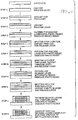
- Fig. 1 shows the principal steps in the method of fabricating two-layered thin film devices without forming any fenestration patterns.
- Multiple layers of thin film device material and sacrificial material are sputter deposited sequentially on a surface of substrate 26, which is an oxidized silicon wafer, in the process chamber.
- Device material can be TiNi, other derivative alloys of TiNi, stainless steel, and the like.
- Shape memory alloys such as TiNi can be sputter deposited, but they cannot be deposited by electroplating. Many non-SMA alloys and metal can be deposited by electroplating to form portions of the devices.
- Sacrificial material can be chromium, aluminum, copper, TiCuAg or any other metal or alloy.
- the process chamber is equipped with two separate targets: one for the thin film device layer and the other for the sacrificial layer.
- the device layer is deposited using DC sputtering and the sacrificial layer using RF sputtering.
- Sputtered thin film alloy can also be achieved by either sputtering from a single alloy target or by co-sputtering from multiple targets.
- Polished and oxidized silicon wafers are used as substrates and are loaded into the chamber which is pumped down to achieve vacuum in a low 10 -7 torr range. Highly polished and flat glass wafer can also be used as the substrate.
- a thin release or sacrificial layer 28 is sputter deposited on the substrate using RF sputtering at argon pressure of about 2 millitorr (1 millitorr is approximately 0.133 Pa) ( Fig. 1 , step A). Thickness of the deposited thin film 28 can be 500 ⁇ (1 Angström is 0.1 nm) or more.
- a thin layer 30 of the device material is sputter deposited on top of the sacrificial layer using DC sputtering at an argon pressure of about 2 millitorr ( Fig. 1 , step B). Thickness of the deposited device layer 30 can be from 1 mm to 50 mm.
- a thin sacrificial layer 32 is then sputter deposited on top of the device layer ( Fig. 1 , step C). Typical thickness of this layer 32 is about 1000 ⁇ .
- This layer plays two roles: 1) it acts as a protective layer for the underlying device layer during subsequent lithography steps, and 2) it acts as a sacrificial layer which in the final steps of fabrication is dissolved away chemically in order to selectively create a pocket between the two device layers.
- a photo mask is typically a high quality chrome coated glass plate with desired device patterns etched on to the chrome layer which finally results in opaque and clear regions correspondingly on the mask plate.
- Designs on the mask determine the final three-dimensional shape of the device. For example, solid triangular designs for cones, rectangular for cylinders, semicircular for hemispheres, etc.
- Mask B contains designs for final definition of the device, fenestration patterns or any other surface pattern which may be needed for the final device.
- Mask A is used to pattern the top sacrificial layer deposited on the wafer described above.
- a thin layer 34 of positive photo resist liquid is spin-coated on the above wafer at about 4000 rpm and baked at 90°C in a clean room convection oven.
- an ultraviolet light mask aligner the wafer and mask A are aligned and the photo resist layer is UV exposed though the mask plate which transfers the patterns from mask A on to the photo resist layer.
- the wafer with exposed photo resist is immersed in developer solution to selectively remove the exposed sections of the photo resist thus creating windows in the photo resist layer on the wafer.
- these windows in the photo resist allow for the selective etching of the sacrificial layer as shown in Fig. 1 , step D.
- the photo resist layer is chemically dissolved away by immersing in a solvent ( Fig. 1 , step E) which also concludes the photolithography process.
- the wafer with the selectively etched sacrificial layer is loaded back into the sputtering chamber which is then pumped down to low 10 -7 torr vacuum.
- the top exposed surface layer is sputter-etched to clean it from any contamination.
- Sputter-etch is a process similar to sputtering except that in the case of sputter-etch the argon ions are accelerated to the substrate surface rather than the target surface.
- High energetic argon ions when operated in sputter-etch mode also remove undesired thin native oxide layer on the surface which may have formed during the lithography process.
- a layer 36 of device material and a sacrificial layer 38 are sputter deposited on the substrate ( Fig. 1 , step F).
- the thickness of these layers may remain the same as in steps B and C.
- the sputtered device material is TiNi or any other shape memory alloy
- the material is heat-treated at 500°C in vacuum for crystallization so that the material exhibits the properties of shape memory alloy and superelasticity.
- the sputtered wafer from above is mounted on a hot plate which is situated in a vacuum chamber. In a reasonable vacuum, the power to the hot plate is turned on and the temperature is monitored at the bottom and top end of the wafer using thermocouples.
- the layer 40 of photo resist is spin-coated to pattern the layers with designs in mask B using the photolithography steps described herein.
- the underlying device layers are also chemically etched with the same mask design in order to define the device's outer features.
- This is followed by the complete removal of photo resist layer 40 ( Fig. 1 , step H).
- the whole wafer with patterned layers is immersed into the chemical etchant to completely dissolve the sacrificial layer ( Fig. 1 , step I), leaving the patterned device layers 30 and 36.
- the etchant for this purpose should be such that it should etch the sacrificial material selective to the device layer. This etching not only separates the devices from the substrate surface but also selectively creates an empty pocket between the two device layers by etching away the sacrificial layer from between.
- Fig. 2 shows the principal steps in the method of fabricating two-layered thin film devices having fenestration patterns etched into the thin film.
- the photo resist layer 42 in Fig. 2 step G is patterned using mask B which contains the necessary fenestration patterns.
- the basic process sequence to fabricate thin film devices with fenestration patterns is similar to that described in connection with Fig. 1 , except for the added designs on mask B.
- sacrificial and device layers are patterned by chemical etching ( Fig. 2 , step G).
- Fig. 3 illustrates the principal steps in a method of the invention for fabricating two-layered thin film devices with both layers having different fenestration patterns.
- the designs in mask A and mask B have been modified to fit the new patterns.
- the photo resist layers as shown in step D and G are patterned using mask plates (mask A and mask B) which contain their own fenestration patterns.
- Fig. 4 illustrates the principal steps in the method of fabricating thin film devices with more than two layers.
- the multiple sputtered layers of sacrificial and device materials are added sequentially.
- the figure. shows an example in which the method fabricates a device with four layers. Such devices may be fabricated with or without fenestration patterns.
- additional layers of sacrificial and device material can be repeatedly sputter deposited and patterned. The number of required mask plates increases proportionally with the number of layers to be patterned.
- the process sequence to fabricate devices with four layers of sputtered thin film is illustrated in Fig. 4 .
- the released multi-layered thin film devices from the steps of the methods in Figs. 1 - 4 are in planar form which may be of various geometric shapes such as triangular, rectangular, semicircular and the like as required by the particular application.
- These multi-layered thin film shapes are then transformed into their corresponding three-dimensional shapes by inserting a suitable stainless steel mandrel (not shown) into the pockets between the layers and re-annealing them at 500°C in vacuum.
- the mandrel is made in a size and shape which is commensurate with the desired three dimensional shape of the end-use device. Re-annealing of the thin film with the mandrel inserted causes the shape-setting according to the shape of the mandrel.
- the resulting shape is the memory shape that the SMA layers forcefully revert to when heated through the phase change transformation temperature.
- the approximate 98°F (36.6°C) blood temperature heats the device through the transformation temperature resulting in it deforming to the conical, cylindrical, hemispherical or other shape which is desired for the particular end-use application.
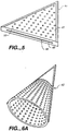
- Fig. 5 illustrates a triangular multi-layered thin film fenestrated planar form structure 44 made in accordance with one method of the invention.
- the top layer 46 is joined with bottom layer 48 along the left and right sides as view in the figure, and creating a pocket between these layers everywhere else.
- Fig. 6A illustrates a thin film conical shell device 52 made after three-dimensional shaping from the planar form of Fig. 5 .
- the shaping step is carried out by inserting a conformable cone shaped mandrel, not shown, into opening 49 of the planar form, and by heat-treating at 500°C in vacuum with the mandrel placed inside.
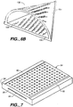
- Fig. 6B illustrates a thin film half-conical shell device 130 made after three-dimensional shaping from a planar form of Fig. 5 .
- the device is formed by deforming one layer 134 into a conical shape while the other layer 136 remains flat.
- a pattern of fenestrations 138 is formed in each layer.
- Fig. 7 illustrates a rectangular multi-layered thin film planar fenestrated form structure 54 made in accordance with one method of the invention.
- the top and bottom layers 56 and 58 of the structure are joined along two opposing sides 60 and 62, and spaced apart to form openings 64 everywhere else.
- Fig. 8A illustrates a thin film cylindrical shell device 66 made after three-dimensional shaping from the planar form of Fig. 7 using a cylindrical shaped mandrel.
- Fig. 8B illustrates a thin film half-cylindrical shell device 140 made by three-dimensional shaping from the planar form of Fig. 7 .
- a pattern of fenestrations 142 are formed in each layer.
- One layer 144 is deformed into a cylindrical shape while the other layer 146 remains flat.
- Fig. 9 illustrates a semi-circular shaped multi-layered thin film planar form structure 68 made in accordance with one method of the invention.
- the top and bottom layers 70 and 72 are joined along the curved sides, and are spaced apart to form an opening 74 everywhere else.
- a pattern of fenestrations 75 are formed in each layer.
- Fenestrations 75 are specifically shaped as slots and positioned to enable the thin film layers to transform from a planar shape into a spherical or spheroidal (meaning the type of shape made by rotating an imaginary curved line, such as an ellipse, about an axis) shape.
- the specific shape and placement of the slots in device 84 is critical because if an unfenestrated layer of a metal or metal alloy material were to be deformed into a spherical or spheroid shell then portions of the layer would be stretched beyond the material's elastic limit and tear.
- the specific shape and positioning of slots 75 is made by forming them in a plurality of transversely spaced apart rows 148, 150.
- the slots in each row are laterally offset a distance D 1 from the slots in the rows adjacent to it.
- the slots in each row are also longitudinally spaced-apart a distance D 2 .
- the distances D 1 and D 2 are selected, depending on factors such as thickness and type of material, to be sufficient to enable deformation of the layer into the three dimensionally curved shape. This is because the layer portions joining the slots are only stretched below the material's elastic limit, while the lateral stretching between the slots in all the rows in combination is sufficient to enable deformation into a spherical or spheroidal shape.
- Fig. 10 illustrates a thin film hemispherical shell device 76 made after three-dimensional shaping from the planar form of Fig. 9 using a hemispherical shaped mandrel.
- Fig. 11 illustrates a superelastic hemispherical SMA thin film fenestrated device 84 made with a plurality of narrow strings 86.
- the strings are formed integral with and in circumferential spaced relationship about the rim of the hemisphere and extend parallel with the longitudinal axis of the device. Suitable dimensions for the hemisphere are a diametrical size on the order of 1 mm to tens of millimeters with the strings each having a width in the range of 50 microns to few millimeters and a film thickness in the range of 1 micrometer to 50 micrometers.
- the strings are made by fabricating a thin film cylindrical shell extending from the hemisphere's rim (all one material).
- the fenestration pattern in the thin film hemisphere is such that it allows to deform into a hemisphere.
- the thin film device is superelastic at body temperature.
- Fig. 12 illustrates placement of the hemispherical thin film device 86 of Fig. 11 within an aneurysm 78 in a manner which covers the neck opening in the blood vessel 80 from which the aneurysm has erupted.
- the thin film device is initially folded and inserted (called loading of the device) into a microcatheter at the room temperature.
- the tubing of the microcatheter prevents the device from opening and the device opens only when the device is pushed out of the microcatheter at body temperature.
- the thin film hemispherical device can be made from a shape memory alloy such as nitinol.
- the superelastic property enables the device to deform as they are guided through the endoluminal spaces and into the aneurysm by suitable means, such as a microcatheter.
- suitable means such as a microcatheter.
- the device When deployed in an aneurysm, the device warms up to the blood temperature and actuates from its folded shape to its original ⁇ memory ⁇ hemispherical shape.
- the strings simply fill the aneurysm volume and keep the hemispherical device in its position.
- the stagnant blood inside the aneurysm volume causes the formation of a thrombosis.
- the resulting thromboembolism in the aneurysm and the presence of the hemispherical thin film device at the neck of the aneurysm block further intrusion of blood into the aneurysm. This results in protection against a life-threatening build up of blood pressure and possible eventual rupture of the aneurysm wall.
- the strings or tentacles of the hemispherical device When initially inserted endolumenally into the human body, the strings or tentacles of the hemispherical device are below their transition temperature in their cold state. In this state they are sufficiently plastic to enable them to be folded, loaded into a microcatheter, dragged through small and sinuous blood vessels in the brain or other part of the body, and deployed in an aneurysm in the manner shown in Fig. 11 .
- the strings When heated by the blood to the transition temperature, the strings have sufficient strength to tangle together but, because of their small size, insufficient strength to straighten out from shape memory recovery so that they do not rupture the wall of the aneurysm.
- the tangled strings will fill the aneurysm volume and accelerate formation of a thrombus within the void. This will stop blood flow into the aneurysm to prevent a rupture of the aneurysm and ultimately a stroke.
- a conical thin film SMA device 88 with integral strings 90 is fabricated using the foregoing processes.
- Device 88 is formed with fenestrations 92 for use as a blood clot retriever device to filter or capture and remove any blood clots in small blood vessels. With the strings this filter device will be folded and loaded into a microcatheter. The microcatheter is then used to drag the folded device through a blood vessel to the site of any blood clot. The device then deploys by unfolding as the SMA recovers to its memory shape responsive to being heated through its transition temperature. The conical basket then captures and removes the clot as the microcatheter is withdrawn.
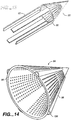
- Fig. 14 shows an SMA thin film fenestrated structure 94 fabricated in accordance with another embodiment comprising a conical shell 96.
- the shell is fabricated similar to that described in connection with Figs. 5-6 and further comprises a plurality, shown as four, of pockets 98 position in spaced relationship about the shell's rim.
- the pockets have openings 100 at the circular rim of the shell. Fabrication method as shown in Fig. 4 is used to fabricate such devices with pockets.
- Fig. 15 shows another version of a blood clot removal device 102 which is comprised of the fenestrated structure 94 of Fig. 14 together with a cage 104.
- the cage comprises a strut 106 which is integrally formed with a plurality of elongated thin fingers or wires 108 equal in number to the number of pockets 100 on the shell.
- the strut and fingers can be formed of any material which is suitable for insertion into and attaching with the pockets, such as SMA, other alloy, metal or polymer.
- the struts and fingers can be formed from a tube using laser cutting and electropolishing techniques.
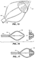
- Fig. 16 shows an initial step in assembly of cage 104 with the shell, which is done before inserting device 102 endolumenally into the body.
- the finger tips are drawn together.
- each tip is moved radially out into register with its corresponding shell pocket.
- the strut and shell are moved toward each other so that the finger tips are inserted into locking engagement with the pockets in the manner shown in Fig. 17 .
- the strut loaded with the thin film device is then inserted into a microcatheter which can be used to drag the device through a blood vessel for capturing and removing any blood clot in the manner described in connection with Fig. 13 .
- fenestrations on the device are small enough to allow blood flow through device 102 while preventing passage of any blood clots.
- fenestration means an opening having rectilinear sides such as rectangular, triangular or the like, or having curvilinear sides such as circular, oval or the like.
- FIGs. 18-20 show an intraocular device 110 fabricated in accordance with another embodiment comprising a thin film structure which provides a means for implanting and anchoring a lens, for example a plastic lens for replacing an incompetent lens, within the human eye.
- the thin film structure is fabricated by the sputtering methods described herein into a circular flat form having top and bottom layers 112 and 114. During fabrication a window 116 is centrally formed in both layers. The outer peripheral edges of the two layers are joined together.
- the inner margins of the layers surrounding the window are axially spaced apart to form an inwardly directed circular empty slot 118, best shown in Fig. 21 .
- a plurality of notches 120 are formed in the layers around the window so that the remaining slot material forms pockets into which the lens can be supported. Then the structure is shaped into the hemispherical shell 122 shown in Fig. 19 by the use of a mandrel and heat treatment.
- device 110 is surgically placed within the eyeball 125 behind the cornea 124 and iris 126.
- the outer rim of the device is fitted between the ring of muscles 128, which would otherwise be attached to the natural lens for the control of focus accommodation.
- a replacement lens 130 of a plastics or other suitable material shown prior to its insertion in Fig. 21 , is fitted with its outer rim seated within the pockets of slot 118 as shown in Figs. 20 and 22 .
- an anastomosis device can be made by fabricating three thin film cylinders or tubing, not shown, having nearly the same diameter, each of which resembles a stent.
- a short segment of one of the cylinders is compressed and inserted into the lumen of each blood vessel end. This cylinder is then allowed to expand so that the lumen is held open.
- the two other thin film cylinders are then expanded and slipped over respective ones of the two ends; these two cylinders are permitted to contract radially.
- the two severed blood. vessel ends are secured between an internal cylinder that presses outward radially, and external cylinders that gently press inward radially. This method of anastomosis is relatively quick, provides an optimum resistance to collapse, and provides a scaffold for healing.
- the methods of fabricating three-dimensional thin film shapes and devices as described may vary according to a specific application. This invention also applies to methods of fabricating thin film devices made from materials other than shape memory alloy which can be sputter deposited. While we have described and illustrated the use of this invention in relation to medical device applications, various other devices for other applications may be created using the methods. While various embodiments of the methods of fabrication have been described, other configurations and embodiments may also be devised within the scope of the invention as set forth in the accompanying claims.
Landscapes
- Health & Medical Sciences (AREA)
- Life Sciences & Earth Sciences (AREA)
- Surgery (AREA)
- Engineering & Computer Science (AREA)
- Biomedical Technology (AREA)
- Veterinary Medicine (AREA)
- Heart & Thoracic Surgery (AREA)
- Vascular Medicine (AREA)
- Animal Behavior & Ethology (AREA)
- General Health & Medical Sciences (AREA)
- Public Health (AREA)
- Medical Informatics (AREA)
- Nuclear Medicine, Radiotherapy & Molecular Imaging (AREA)
- Molecular Biology (AREA)
- Reproductive Health (AREA)
- Physics & Mathematics (AREA)
- Transplantation (AREA)
- Oral & Maxillofacial Surgery (AREA)
- Cardiology (AREA)
- Optics & Photonics (AREA)
- Neurosurgery (AREA)
- Orthopedic Medicine & Surgery (AREA)
- Prostheses (AREA)
Description
- This invention relates to methods for manufacturing devices of three-dimensional shapes using two-dimensional micro-electro-mechanical system (MEMS) techniques. The invention can be applied to materials with or without shape memory or superelastic properties, and has widespread applications, especially for fields and industries that have a demand for a high degree of miniaturization of devices and equipment.
- In recent years many medical devices have been introduced that incorporate shape memory and superelastic materials, especially titanium nickel alloys often referred to as TiNi or Nitinol. Two principal products are guidewires for catheters and stents used in the treatment of vascular disease. Use of Nitinol in stents fabricated from small diameter Nitinol tubing has grown rapidly.
- Fabrication of stents includes the operations of laser cutting, expansion, heat treatment, and electropolishing. These processes are labor intensive arid costly. Stents made from tubing are generally lacking in flexibility required to treat small blood vessels in the brain that must be accessed intralumenally through tortuous distal paths in the carotid artery.
- Accordingly there is a need for improved devices to be used in the intracranial vasculature. The present invention provides an alternative method of fabricating tools for endolumenal use that result in devices that are small, flexible, inexpensive to make, smooth-surfaced, chemically resistant, and possess superelastic and shape memory properties. These devices include stents, filters, blood clot retrievers, aneurysm closures,
and anastomosis devices for use in conjunction with blood vessel transplants. - Thin TiNi film has desirable characteristics for fabricating these devices, especially because it can be rolled, folded, or otherwise compressed for insertion through micro-catheters.
- Production of complete systems for minimally invasive vascular treatment involves joining of components by welding, brazing, soldering, and adhesives. Superior performance can be achieved if the number of such attachments is minimized. Additionally, welding of thin film (micrometers thick) presents novel problems. It is desirable to make the device all in one piece to achieve maximum flexibility, strength, and minimal thrombo-genicity.
- The most common method of producing thin metal films is by vacuum sputtering, generally onto a planar substrate. Sputtering onto three-dimensional substrates can be accomplished by rotation of the substrate in or near the plasma, and by cylindrical sputtering. While it has been shown that it is possible to sputter three-dimensional shapes, it is also known that the material thus produced by this method is not of the highest quality, and the methods do not lend themselves to production of large numbers of devices at low cost.
- In cylindrical sputtering it is difficult to achieve the correct chemical composition. For intravascular use, the transition temperature should be below body temperature, 36.6°C, to take advantage of superelasticity.
- In three-dimensional deposition it is difficult to achieve good crystal structure of the deposited thin film alloy. This requires shielding to produce lin-of-sight normal deposition, otherwise columnar structure appears with poor intra-crystalline and inter-crystalline adhesion. Brittleness results.
- It is also difficult to remove the three-dimensional structure from the substrate. Etchants must be extremely selective, and must not interact with the thin film material, generally TiNi or TiNi-based.
- Miniature devices made of free-standing thin film shape memory alloys such as Nitinol have potential applications in medicine, particularly in minimally invasive surgery of the vasculature. For a majority of endolumenal applications it is essential that these devices have three-dimensional shapes, i.e. cones, cylinders, and hemispheres, to take advantage of superelastic and shape memory properties. In applications relating to tissue engineering, these three-dimensional shapes of Nitinol thin film can be used as a base structural material or scaffold on which to grow artificial tissue cells. For example, tissue grown on a thin film cylinder will produce an artificial blood vessel in a tubular shape.
- The most practical method of creating thin films of shape memory alloy is by vacuum sputtering. Sputtering onto three-dimensional substrates is wasteful, slow, and subject to difficulties not encountered in planar deposition.
- The need has therefore been recognized for medical device fabrication methods which obviate the foregoing and other limitations and disadvantages of prior art fabrication methods and devices of the type described. Despite the various fabrication methods and devices in the prior art, there has heretofore not been provided a suitable and attractive solution to these problems.
- Our previous patent application
WO 98/53362 A2 - The article John J Gill et al: "Three-Dimensional Thin-Film Shape Memory Alloy Microactuator With Two-Way Effect" Journal of Microelectromechanical Systems, IEEE Service Center, Piscataway, NJ, US, vol. 11, no. 1, 1 February 2002, XPO11034685, ISSN: 1057-7157 discloses a method of forming a freestanding NiTi membrane in which an NiTi film is deposited on the front side of a silicon wafer annealed, and patterned by wet etching, with the remaining silicon beneath the patterned NiTi film then being removed.
-
WO 99/16387 A1 - It is a general object of the invention to provide methods of manufacturing devices of three-dimensional shapes using two-dimensional micro-electro-mechanical techniques.
- Another object is to provide methods to make multiple layered three-dimensional shapes with pockets created selectively between the layers, such as for endovascular, endolumenal, intracranial, and intraocular medical applications.
- The prior art limitations and limitations described above are overcome in the present invention by methods that comprise planar material deposition that has advantages including high deposition rates, improved control of composition, and use of large substrates to make batches of devices rather than individual devices. This leads to a practical manufacturing method for large volume production.
- The methods of the invention comprise the removal of material by chemical means that, combined with planar sputter deposition of multiple layers, photolithography, and heat treatment, enables the fabrication of hollow shapes having thin film surfaces of sufficiently small size for use in medicine, including endovascular, endolumenal, intracranial, and intraocular applications.
-
-
Fig. 1 is a block diagram showing the general steps in the method of one embodiment of the invention. -
Fig. 2 is a block diagram showing the general steps in the method of another embodiment of the invention. -
Fig. 3 is a brock diagram showing the general steps in the method of another embodiment of the invention. -
Fig. 4 is a block diagram showing the general steps in the method of another embodiment of the invention. -
Fig. 5 is a perspective view of a multi-layered thin film triangular planar form before three-dimensional shaping. -
Fig. 6A is a perspective view of a cone made by three-dimensional shaping from the planar form ofFig. 5 . -
Fig. 6B is a perspective view of a half-conical shell device fabricated in accordance with another embodiment. -
Fig. 7 is a perspective view of a multi-layered thin film rectangular planar form before three-dimensional shaping. -
Fig. 8A is a perspective view of a cylinder made by three-dimensional shaping from the planar form ofFig. 7 . -
Fig. 8B illustrates illustrates a thin film half-cylindrical shell device fabricated accordance with another embodiment. -
Fig. 9 is a perspective view of a multi-layered thin film semicircular planar form before three-dimensional shaping. -
Fig. 10 is a perspective view of a hemisphere made by three-dimensional shaping from the planar form ofFig. 9 . -
Fig. 11 is a perspective view of a three dimensional hemispherical shell device fabricated in accordance with another embodiment. -
Fig. 12 is a partially cut-away perspective view showing the insertion of the hemispherical shell ofFig. 11 into an aneurysm of the human body. -
Fig. 13 is a perspective view of a cone device with integral strings or tentacles fabricated in accordance with another embodiment. -
Fig. 14 is a perspective view of a fenestrated conical device shaped with pockets for seating strings fabricated in accordance with another embodiment. -
Fig. 15 is a perspective view of the conical device ofFig. 14 with strings seated shaped in the pockets. -
Fig. 16 is a schematic view in cross section showing one step in assembly of the conical device ofFig. 15 . -
Fig. 17 is a schematic view in cross section, showing another step in assembly of the conical device ofFig. 15 . -
Fig. 18 is a perspective view of a multi-layered thin film circular planar form fabricated in accordance with another embodiment. -
Fig. 19 is a perspective view of a hemispherical ocular device made by three-dimensional shaping from the planar form ofFig. 16 . -
Fig. 20 is a schematic view in longitudinal section a human eye implanted with the device ofFig 19 . -
Fig. 21 is a schematic view in cross section showing one step in the fitment of a lens into the ocular device ofFig. 19 . -
Fig. 22 is a schematic view in cross section showing another step in the fitment of a lens into the ocular device ofFig. 19 . - In a broad aspect of the invention, three-dimensional shapes, especially cones, cylinders and hemispheres, are made by methods which comprise opening two-dimensional, multiple-layered planar structures of micrometer (mm) size. This enables the design and development of shape memory thin film actuated micro-apparatus as therapeutic devices for the medical industry. One such example is the development of an endovascular apparatus for the treatment of intracranial aneurysms. The methods of the invention will also enable the design of medical endolumenal implants for various endovascular as well as other medical applications. In most of these methods, the principle functional materials used are thin film TiNi (also termed NITINOL) which is an alloy of nearly equal atomic compositions of titanium and nickel, or its derivatives such as CuAlNi or TiNiPd alloys. These shape memory alloys (also termed SMA) have the properties of shape memory effect and superelasticity. The superelastic properties of SMA are discussed in the publication: K. Otsuka, C.M. Wayman, eds. Shape Memory Materials, Cambridge University Press 1998 at pages 27 et. seq.
- The SMA material is annealed into a crystalline state so that it undergoes a crystalline phase transformation from martensite to austenite when heated through the material's phase change transformation temperature. When below that temperature the material can be plastically deformed from its memory shape in response to a stress. When the deformed SMA material is heated through the transformation temperature, it forcefully reverts to its memory shape while exerting considerable force. The transformation temperature of TiNi having equal atomic compositions of the two elements can he made in the range of about 50 to 70°C, and suitable adjustments of the alloy compositions can achieve transformation temperatures ranging from 0°C to 100°C. During the alloying process, a third metal such as hafnium or palladium can be amalgamated with the Ti and Ni elements to raise the transition temperature, while iron or vanadium can be amalgamated with the Ti and Ni to lower the transition temperature, as required for particular applications.
- When the SMA composition of a three-dimensional shape is made such that the transformation temperature is below the 36.6°C (normal temperature of the human body) then the SMA becomes superelastic when heated by blood temperature through the transformation temperature. As a superelastic, the device while in its high temperature phase can be stressed to deform as much as from 3 to 5% without being damaged. This superelasticity enables the device to deform enough for insertion through endolumenal structures of the body, such as being folded under compression within a microcatheter. The stress is removed by withdrawing the device from the microcatheter, allowing it to recover its shape.
- Thin film devices may be fabricated by using microfabrication techniques involving sputtering of metals and TiNi alloys. Typically these thin layers of metal and metal alloys are sputtered using DC magnetron and RF sputtering techniques. The planar thin film structures are built up layer-by-layer through sputter deposition. Alternating layers of TiNi and sacrificial material are sputtered on a smooth flat surface of a substrate, for example a silicon wafer. TiNi and the sacrificial material layers are selectively patterned by micro-photolithography techniques in which a thin layer of photo resist material is spin-coated and used to selectively remove the material to form a pattern on these layers.
- Appropriate designs, to construct various shapes, are printed on photo masks which are eventually used for creating the desired patterns on the TiNi and sacrificial material layers. These multi-layered thin film structures are heat treated at temperature of 500°C in order to crystallize sputtered TiNi material. TiNi, after annealing, exhibits the desired shape memory and superelastic properties. These planar multi-layered thin film structures are transformed into various three-dimensional shapes by insertion of shape forming mandrels and heat-treatment.
- For various applications, three-dimensional shapes of thin film are required to have certain fenestration patterns. As used herein, the term thin film means a film with of thickness less than 50 microns. Fenestrations patterns are generated on these devices in their planar form using micro-photolithography techniques. Since these fenestration patterns are generated photochemically, the sizes and shapes of these patterns can be controlled very precisely and uniformly. The diameters of the fenestrations are sufficient to allow blood cells to pass by which block larger size clots, and can be in the range of 30mm to 40mm. Very sharp and well defined edge quality is thereby achieved. These micron-scaled fenestration patterns are generated on thin film by spin coating a thin layer of photo resist which is then patterned using a photomask glass plate containing the fenestration patterns in the form of clear and opaque regions. This allows the etching of thin films, both TiNi and sacrificial layers, from the selective regions. Appropriate etching solutions are used in order to etch different metal layers, selectively, without damaging the other metal layer. After generating the final fenestration patterns and final device features, the multi-layered thin film devices are released from the substrate by chemically dissolving the sacrificial layers away.
- The methods of the invention for forming three-dimensional shapes of thin film can be extended from two layers to any number of thin film layers. Various ingenious features are generated and added on to a three dimensional shape by sputtering more than two layers of thin film material. Pockets between two layers on a three-dimensional surface are by sputtering multiple layers of thin film material by selectively etching a sacrificial layer. The pockets between the two thin film layers in the final device are used for insertion or attachment of outside structures such as a catheter or wire to the three-dimensional thin film devices.
- The methods of the invention for forming three-dimensional shapes of thin film can also be extended to create different fenestration patterns in each layer of thin film.
- Among the three-dimensional thin film shapes and their possible use for medical applications are the following. Fenestrated cone shapes are intended to be used for retrieval of blood clots, particularly clots causing ischemic stroke. Cylinder shapes are intended for use as stents to support blood vessels from collapse and stenosis, and to permit treatment of intracranial aneurysms. Cylindrical shapes are also intended for use as a scaffold structure for making artificially grown blood vessels of all sizes. Hemispherical shaped structures are for insertion into aneurysms to isolate them from blood flow in parent blood vessels. Dome-shaped structures having multiple layers of thin film are intended to be used in intraocular devices for lens implantation. Pockets and channels formed between the two thin film layers enable the attachment of a lens onto a dome-like thin film structure for use in ocular applications.
- Cones or cylinders which are formed from more than two layers of thin film to create channels (or pockets) between the two layers allow the insertion of an outer structure into the thin film structure. In the context of blood clot retrieval devices, a set of such pockets are used as means for attaching wires or other external parts of a catheter to the thin film cone and cylinders.
- Multiple-part devices of the type described are used for osculature of blood vessels. A short segment of fenestrated cylinder is inserted into each end of a pair of blood vessels to be joined, in such a way that they exert an outward pressure on the blood vessel lumen tending to keep it open and to return it to an open shape when crushed. A third cylinder, having a larger diameter, is then placed over the ends. This member will exert an inward pressure. The result is an anastomosis of the two blood vessel ends, in which the blood vessel wall is gently pressed between the two inner cylinders and the outer cylinder. The outer cylinder will be stretched so that when it is placed it gently forces the two ends of the blood vessel against each other to form a seal and to promote healing.
- Deploying or implanting medical devices using micro-catheters through tortuous small blood vessels, in the brain for example, requires devices that are extremely flexible and miniaturized. Such flexible and miniaturized devices are made by the thin film deposition methods of the invention creating extremely thin films with thickness less than 50 micrometers. Although thin film can be fabricated using several deposition techniques, sputter deposition techniques are mainly used for fabricating thin film stents.
- In the invention, thin film sputtering methods involve three basic steps: 1) generation of the atomic or ionic species from the metal or alloy material target, 2) transport of these species from the target to a substrate through a gas or a plasma medium, and 3) condensation of these species on the substrate surface to form a solid thin film. In the context of this invention, the target can be of any metal or metal alloys, the substrate can be a polished silicon or glass wafer and argon gas can be used to generate an intense plasma.
- To form the devices, thin film is sputtered in a process chamber which contains the target material and a rotating table to mount the substrates. In the invention, since the devices are fabricated using a multi-layered thin film system, the process chamber is capable of accommodating multiple sputtering targets. The chamber allows sputtering from one or all the targets in both RF and DC sputtering mode. In the process chamber, vacuum in the range of low 10-7 torr (1 torr is approximately 133 Pa) is accomplished by the help of one or more vacuum pumps such as a mechanical pump, cryo pump or turbo molecular pump. Argon gas (or other inert gas) at a low pressure (around few millitorr) is introduced into the chamber. Upon applying a high voltage to the target material from a DC or an RF power supply, a glow discharge is created which dissociates the argon atoms into an intense cloud of ions called plasma. These ions in the plasma are accelerated to the target material and are capable of dislodging atoms from the target surface. These dislodged atoms condense on the substrate surface which is mounted on the table, thereby depositing thin film on the substrate.
-
Fig. 1 shows the principal steps in the method of fabricating two-layered thin film devices without forming any fenestration patterns. Multiple layers of thin film device material and sacrificial material are sputter deposited sequentially on a surface ofsubstrate 26, which is an oxidized silicon wafer, in the process chamber. Device material can be TiNi, other derivative alloys of TiNi, stainless steel, and the like. Shape memory alloys such as TiNi can be sputter deposited, but they cannot be deposited by electroplating. Many non-SMA alloys and metal can be deposited by electroplating to form portions of the devices. Sacrificial material can be chromium, aluminum, copper, TiCuAg or any other metal or alloy. To create such multiple layers, the process chamber is equipped with two separate targets: one for the thin film device layer and the other for the sacrificial layer. Preferably the device layer is deposited using DC sputtering and the sacrificial layer using RF sputtering. Sputtered thin film alloy can also be achieved by either sputtering from a single alloy target or by co-sputtering from multiple targets. Polished and oxidized silicon wafers are used as substrates and are loaded into the chamber which is pumped down to achieve vacuum in a low 10-7 torr range. Highly polished and flat glass wafer can also be used as the substrate. - As shown in
Fig. 1 , a thin release orsacrificial layer 28 is sputter deposited on the substrate using RF sputtering at argon pressure of about 2 millitorr (1 millitorr is approximately 0.133 Pa) (Fig. 1 , step A). Thickness of the depositedthin film 28 can be 500Å (1 Angström is 0.1 nm) or more. Athin layer 30 of the device material is sputter deposited on top of the sacrificial layer using DC sputtering at an argon pressure of about 2 millitorr (Fig. 1 , step B). Thickness of the depositeddevice layer 30 can be from 1 mm to 50 mm. A thinsacrificial layer 32 is then sputter deposited on top of the device layer (Fig. 1 , step C). Typical thickness of thislayer 32 is about 1000Å. This layer plays two roles: 1) it acts as a protective layer for the underlying device layer during subsequent lithography steps, and 2) it acts as a sacrificial layer which in the final steps of fabrication is dissolved away chemically in order to selectively create a pocket between the two device layers. - For making three-dimensional thin film shapes as shown in
Figs 5 to 10 , two suitable photo masks (mask A and mask B, both not shown) with appropriate pattern designs are required. A photo mask is typically a high quality chrome coated glass plate with desired device patterns etched on to the chrome layer which finally results in opaque and clear regions correspondingly on the mask plate. Designs on the mask determine the final three-dimensional shape of the device. For example, solid triangular designs for cones, rectangular for cylinders, semicircular for hemispheres, etc. Mask B contains designs for final definition of the device, fenestration patterns or any other surface pattern which may be needed for the final device. Mask A is used to pattern the top sacrificial layer deposited on the wafer described above. - To pattern the above sputtered wafer with designs on mask A, typical steps of micro-photolithography technique are followed. A
thin layer 34 of positive photo resist liquid is spin-coated on the above wafer at about 4000 rpm and baked at 90°C in a clean room convection oven. Using an ultraviolet light mask aligner, the wafer and mask A are aligned and the photo resist layer is UV exposed though the mask plate which transfers the patterns from mask A on to the photo resist layer. The wafer with exposed photo resist is immersed in developer solution to selectively remove the exposed sections of the photo resist thus creating windows in the photo resist layer on the wafer. When immersed in a chemical etchant, these windows in the photo resist allow for the selective etching of the sacrificial layer as shown inFig. 1 , step D. After patterning the sacrificial layer, the photo resist layer is chemically dissolved away by immersing in a solvent (Fig. 1 , step E) which also concludes the photolithography process. - The wafer with the selectively etched sacrificial layer is loaded back into the sputtering chamber which is then pumped down to low 10-7 torr vacuum. In the chamber, the top exposed surface layer is sputter-etched to clean it from any contamination. Sputter-etch is a process similar to sputtering except that in the case of sputter-etch the argon ions are accelerated to the substrate surface rather than the target surface. High energetic argon ions when operated in sputter-etch mode also remove undesired thin native oxide layer on the surface which may have formed during the lithography process. Followed by the sputter-etch, another
layer 36 of device material and asacrificial layer 38 are sputter deposited on the substrate (Fig. 1 , step F). The thickness of these layers may remain the same as in steps B and C. - Where the sputtered device material is TiNi or any other shape memory alloy, the material is heat-treated at 500°C in vacuum for crystallization so that the material exhibits the properties of shape memory alloy and superelasticity. To achieve this, the sputtered wafer from above is mounted on a hot plate which is situated in a vacuum chamber. In a reasonable vacuum, the power to the hot plate is turned on and the temperature is monitored at the bottom and top end of the wafer using thermocouples.
- As illustrated in
Fig. 1 , step G, thelayer 40 of photo resist is spin-coated to pattern the layers with designs in mask B using the photolithography steps described herein. In this step, after etching the topsacrificial layer 38, the underlying device layers are also chemically etched with the same mask design in order to define the device's outer features. This is followed by the complete removal of photo resist layer 40 (Fig. 1 , step H). To separate the devices from the surface of the substrate, the whole wafer with patterned layers is immersed into the chemical etchant to completely dissolve the sacrificial layer (Fig. 1 , step I), leaving the patterned device layers 30 and 36. The etchant for this purpose should be such that it should etch the sacrificial material selective to the device layer. This etching not only separates the devices from the substrate surface but also selectively creates an empty pocket between the two device layers by etching away the sacrificial layer from between. -
Fig. 2 shows the principal steps in the method of fabricating two-layered thin film devices having fenestration patterns etched into the thin film. To create fenestration patterns, the photo resistlayer 42 inFig. 2 , step G is patterned using mask B which contains the necessary fenestration patterns. The basic process sequence to fabricate thin film devices with fenestration patterns is similar to that described in connection withFig. 1 , except for the added designs on mask B. After patterning the photo resist layer with fenestrations, sacrificial and device layers are patterned by chemical etching (Fig. 2 , step G). -
Fig. 3 illustrates the principal steps in a method of the invention for fabricating two-layered thin film devices with both layers having different fenestration patterns. The designs in mask A and mask B have been modified to fit the new patterns. To create different fenestration patterns in each layer, the photo resist layers as shown in step D and G are patterned using mask plates (mask A and mask B) which contain their own fenestration patterns. -
Fig. 4 illustrates the principal steps in the method of fabricating thin film devices with more than two layers. The multiple sputtered layers of sacrificial and device materials are added sequentially. The figure. shows an example in which the method fabricates a device with four layers. Such devices may be fabricated with or without fenestration patterns. Following the method ofFigs. 1 and2 , additional layers of sacrificial and device material can be repeatedly sputter deposited and patterned. The number of required mask plates increases proportionally with the number of layers to be patterned. The process sequence to fabricate devices with four layers of sputtered thin film is illustrated inFig. 4 . - The released multi-layered thin film devices from the steps of the methods in
Figs. 1 - 4 are in planar form which may be of various geometric shapes such as triangular, rectangular, semicircular and the like as required by the particular application. These multi-layered thin film shapes are then transformed into their corresponding three-dimensional shapes by inserting a suitable stainless steel mandrel (not shown) into the pockets between the layers and re-annealing them at 500°C in vacuum. The mandrel is made in a size and shape which is commensurate with the desired three dimensional shape of the end-use device. Re-annealing of the thin film with the mandrel inserted causes the shape-setting according to the shape of the mandrel. In case of the device material being a shape memory alloy, the resulting shape is the memory shape that the SMA layers forcefully revert to when heated through the phase change transformation temperature. In the human body the approximate 98°F (36.6°C) blood temperature heats the device through the transformation temperature resulting in it deforming to the conical, cylindrical, hemispherical or other shape which is desired for the particular end-use application. -
Fig. 5 illustrates a triangular multi-layered thin film fenestratedplanar form structure 44 made in accordance with one method of the invention. Thetop layer 46 is joined withbottom layer 48 along the left and right sides as view in the figure, and creating a pocket between these layers everywhere else. -
Fig. 6A illustrates a thin filmconical shell device 52 made after three-dimensional shaping from the planar form ofFig. 5 . The shaping step is carried out by inserting a conformable cone shaped mandrel, not shown, into opening 49 of the planar form, and by heat-treating at 500°C in vacuum with the mandrel placed inside. -
Fig. 6B illustrates a thin film half-conical shell device 130 made after three-dimensional shaping from a planar form ofFig. 5 . The device is formed by deforming onelayer 134 into a conical shape while theother layer 136 remains flat. A pattern offenestrations 138 is formed in each layer. -
Fig. 7 illustrates a rectangular multi-layered thin film planarfenestrated form structure 54 made in accordance with one method of the invention. The top andbottom layers sides openings 64 everywhere else. -
Fig. 8A illustrates a thin filmcylindrical shell device 66 made after three-dimensional shaping from the planar form ofFig. 7 using a cylindrical shaped mandrel. -
Fig. 8B illustrates a thin film half-cylindrical shell device 140 made by three-dimensional shaping from the planar form ofFig. 7 . A pattern offenestrations 142 are formed in each layer. Onelayer 144 is deformed into a cylindrical shape while the other layer 146 remains flat. -
Fig. 9 illustrates a semi-circular shaped multi-layered thin filmplanar form structure 68 made in accordance with one method of the invention. The top andbottom layers fenestrations 75 are formed in each layer. -
Fenestrations 75 are specifically shaped as slots and positioned to enable the thin film layers to transform from a planar shape into a spherical or spheroidal (meaning the type of shape made by rotating an imaginary curved line, such as an ellipse, about an axis) shape. The specific shape and placement of the slots indevice 84 is critical because if an unfenestrated layer of a metal or metal alloy material were to be deformed into a spherical or spheroid shell then portions of the layer would be stretched beyond the material's elastic limit and tear. In the invention, the specific shape and positioning ofslots 75 is made by forming them in a plurality of transversely spaced apartrows -
Fig. 10 illustrates a thin filmhemispherical shell device 76 made after three-dimensional shaping from the planar form ofFig. 9 using a hemispherical shaped mandrel. -
Fig. 11 illustrates a superelastic hemispherical SMA thin filmfenestrated device 84 made with a plurality ofnarrow strings 86. The strings are formed integral with and in circumferential spaced relationship about the rim of the hemisphere and extend parallel with the longitudinal axis of the device. Suitable dimensions for the hemisphere are a diametrical size on the order of 1 mm to tens of millimeters with the strings each having a width in the range of 50 microns to few millimeters and a film thickness in the range of 1 micrometer to 50 micrometers. In this embodiment, the strings are made by fabricating a thin film cylindrical shell extending from the hemisphere's rim (all one material). Then parallel, longitudinal extending strings are formed by the photolithography and etching processes. The fenestration pattern in the thin film hemisphere is such that it allows to deform into a hemisphere. The thin film device is superelastic at body temperature. -
Fig. 12 illustrates placement of the hemisphericalthin film device 86 ofFig. 11 within ananeurysm 78 in a manner which covers the neck opening in theblood vessel 80 from which the aneurysm has erupted. The thin film device is initially folded and inserted (called loading of the device) into a microcatheter at the room temperature. The tubing of the microcatheter prevents the device from opening and the device opens only when the device is pushed out of the microcatheter at body temperature. For this application, the thin film hemispherical device can be made from a shape memory alloy such as nitinol. The superelastic property enables the device to deform as they are guided through the endoluminal spaces and into the aneurysm by suitable means, such as a microcatheter. When deployed in an aneurysm, the device warms up to the blood temperature and actuates from its folded shape to its original ÒmemoryÓ hemispherical shape. The strings simply fill the aneurysm volume and keep the hemispherical device in its position. The stagnant blood inside the aneurysm volume causes the formation of a thrombosis. The resulting thromboembolism in the aneurysm and the presence of the hemispherical thin film device at the neck of the aneurysm block further intrusion of blood into the aneurysm. This results in protection against a life-threatening build up of blood pressure and possible eventual rupture of the aneurysm wall. - When initially inserted endolumenally into the human body, the strings or tentacles of the hemispherical device are below their transition temperature in their cold state. In this state they are sufficiently plastic to enable them to be folded, loaded into a microcatheter, dragged through small and sinuous blood vessels in the brain or other part of the body, and deployed in an aneurysm in the manner shown in
Fig. 11 . When heated by the blood to the transition temperature, the strings have sufficient strength to tangle together but, because of their small size, insufficient strength to straighten out from shape memory recovery so that they do not rupture the wall of the aneurysm. The tangled strings will fill the aneurysm volume and accelerate formation of a thrombus within the void. This will stop blood flow into the aneurysm to prevent a rupture of the aneurysm and ultimately a stroke. - As shown in
Fig. 13 , a conical thinfilm SMA device 88 with integral strings 90 is fabricated using the foregoing processes.Device 88 is formed withfenestrations 92 for use as a blood clot retriever device to filter or capture and remove any blood clots in small blood vessels. With the strings this filter device will be folded and loaded into a microcatheter. The microcatheter is then used to drag the folded device through a blood vessel to the site of any blood clot. The device then deploys by unfolding as the SMA recovers to its memory shape responsive to being heated through its transition temperature. The conical basket then captures and removes the clot as the microcatheter is withdrawn. -
Fig. 14 shows an SMA thin filmfenestrated structure 94 fabricated in accordance with another embodiment comprising aconical shell 96. The shell is fabricated similar to that described in connection withFigs. 5-6 and further comprises a plurality, shown as four, ofpockets 98 position in spaced relationship about the shell's rim. The pockets haveopenings 100 at the circular rim of the shell. Fabrication method as shown inFig. 4 is used to fabricate such devices with pockets. -
Fig. 15 shows another version of a bloodclot removal device 102 which is comprised of thefenestrated structure 94 ofFig. 14 together with acage 104. The cage comprises astrut 106 which is integrally formed with a plurality of elongated thin fingers orwires 108 equal in number to the number ofpockets 100 on the shell. The strut and fingers can be formed of any material which is suitable for insertion into and attaching with the pockets, such as SMA, other alloy, metal or polymer. The struts and fingers can be formed from a tube using laser cutting and electropolishing techniques. -
Fig. 16 shows an initial step in assembly ofcage 104 with the shell, which is done before insertingdevice 102 endolumenally into the body. In this stage the finger tips are drawn together. Then each tip is moved radially out into register with its corresponding shell pocket. Then the strut and shell are moved toward each other so that the finger tips are inserted into locking engagement with the pockets in the manner shown inFig. 17 . The strut loaded with the thin film device is then inserted into a microcatheter which can be used to drag the device through a blood vessel for capturing and removing any blood clot in the manner described in connection withFig. 13 . The fenestrations on the device are small enough to allow blood flow throughdevice 102 while preventing passage of any blood clots. As used herein, fenestration means an opening having rectilinear sides such as rectangular, triangular or the like, or having curvilinear sides such as circular, oval or the like. - In addition to the fenestration patterns, pockets between the two layers can be created by the use of sacrificial layers as shown. Thus,
Figs. 18-20 show anintraocular device 110 fabricated in accordance with another embodiment comprising a thin film structure which provides a means for implanting and anchoring a lens, for example a plastic lens for replacing an incompetent lens, within the human eye. The thin film structure is fabricated by the sputtering methods described herein into a circular flat form having top andbottom layers window 116 is centrally formed in both layers. The outer peripheral edges of the two layers are joined together. The inner margins of the layers surrounding the window are axially spaced apart to form an inwardly directed circularempty slot 118, best shown inFig. 21 . A plurality ofnotches 120 are formed in the layers around the window so that the remaining slot material forms pockets into which the lens can be supported. Then the structure is shaped into thehemispherical shell 122 shown inFig. 19 by the use of a mandrel and heat treatment. - As shown in
Fig. 20 ,device 110 is surgically placed within theeyeball 125 behind thecornea 124 andiris 126. The outer rim of the device is fitted between the ring ofmuscles 128, which would otherwise be attached to the natural lens for the control of focus accommodation. Then areplacement lens 130 of a plastics or other suitable material, shown prior to its insertion inFig. 21 , is fitted with its outer rim seated within the pockets ofslot 118 as shown inFigs. 20 and22 . - In another embodiment employing the methods herein an anastomosis device can be made by fabricating three thin film cylinders or tubing, not shown, having nearly the same diameter, each of which resembles a stent. To join two blood vessel ends, a short segment of one of the cylinders is compressed and inserted into the lumen of each blood vessel end. This cylinder is then allowed to expand so that the lumen is held open. The two other thin film cylinders are then expanded and slipped over respective ones of the two ends; these two cylinders are permitted to contract radially. Upon completion of the procedure, the two severed blood. vessel ends are secured between an internal cylinder that presses outward radially, and external cylinders that gently press inward radially. This method of anastomosis is relatively quick, provides an optimum resistance to collapse, and provides a scaffold for healing.
- The methods of fabricating three-dimensional thin film shapes and devices as described may vary according to a specific application. This invention also applies to methods of fabricating thin film devices made from materials other than shape memory alloy which can be sputter deposited. While we have described and illustrated the use of this invention in relation to medical device applications, various other devices for other applications may be created using the methods. While various embodiments of the methods of fabrication have been described, other configurations and embodiments may also be devised within the scope of the invention as set forth in the accompanying claims.
Claims (12)
- A method of fabricating a three-dimensional thin film device from a two-dimensional deposition of material, comprising the steps of:depositing a first release layer (28) on a substrate (26);sputter depositing a thin film base layer (30) on the first release layer;depositing an intermediate sacrificial layer (32) on top of the base layer;patterning the sacrificial layer;sputter depositing a thin film second layer (36) on top of the device layer and sacrificial layer, the base and second layers each being formed of a device material selected from the group consisting of: a device material which is of the same type of material for both layers, and a device material for the base layer which is of a different type of material from a device material for the second layer, the base and second layers each having first and second portions;etching the sacrificial layer and the first release layer to leave an empty pocket between the base layer and second layer and to release the device from the substrate; andinserting a mandrel into the pocket to transform the device into a desired three-dimensional shape; andheating the device while the mandrel is inserted into the pocket.
- A method as in claim 1 including the step of forming the intermediate sacrificial layer (32) of a material selected from the group consisting of chromium, aluminum, copper and TiCuAg.
- A method as in claim 1 in which the steps of depositing the base (30) and second (36) layers are carried out by forming the device material of a shape memory alloy.
- A method as in claim 1 and further comprising the step of forming fenestrations (75, 142) in at least one of the base and second layers.
- A method as in claim 1 and further comprising the step of depositing a third release layer (38) on the second base layer (36), removing a first portion of the third release layer leaving another pattern comprising a second portion that remains of the third release layer, depositing a third base layer of the device material on the first and second portions of the third release layer while causing a portion of the second base layer of the device material to join with a portion of the third base layer of device material which is not covered by the second portion of the third release layer.
- A method as in claim 1 comprising the steps of forming the base (30) and second (36) layers into a planar form structure having a shape selected from the group consisting of polygonal and curvilinear.
- A method as in claim 6 in which the polygonal shape is selected from the group consisting of triangular and rectangular.
- A method as in claim 6 in which the curvilinear shape is selected from the group consisting of semicircular and circular.
- A method as in claim 1 and further including the step of forming a plurality of fenestrations (75, 142) through at least one of the base and second layers while positioning the fenestrations in a plurality of transversely spaced apart rows and with the fenestrations in each row being longitudinally spaced a first distance apart and further with the fenestrations in one row being longitudinal offset a second distance from the fenestrations in the rows adjacent to the one row, the first and second distances being sufficient to enable deformation of the one layer into a three dimensionally curved shape.
- A method as in claim 9 and further including the step of deforming the one layer into a three dimensionally curved shape
- A method as in claim 10 and in which the deforming step is carried out by deforming the one layer into at least a portion of a shape selected from the group consisting of a sphere and a spheroid.
- A method as in claim 10 in which the forming step is carried out by forming the fenestrations (75, 142) into slot shapes.
Applications Claiming Priority (3)
| Application Number | Priority Date | Filing Date | Title |
|---|---|---|---|
| US10/198,654 US6746890B2 (en) | 2002-07-17 | 2002-07-17 | Three dimensional thin film devices and methods of fabrication |
| US198654 | 2002-07-17 | ||
| PCT/US2003/021931 WO2004008504A1 (en) | 2002-07-17 | 2003-07-15 | Three dimensional thin film devices and methods of fabrication |
Publications (3)
| Publication Number | Publication Date |
|---|---|
| EP1532663A1 EP1532663A1 (en) | 2005-05-25 |
| EP1532663A4 EP1532663A4 (en) | 2007-09-26 |
| EP1532663B1 true EP1532663B1 (en) | 2017-11-15 |
Family
ID=30115162
Family Applications (1)
| Application Number | Title | Priority Date | Filing Date |
|---|---|---|---|
| EP03764605.6A Expired - Lifetime EP1532663B1 (en) | 2002-07-17 | 2003-07-15 | Three dimensional thin film device fabrication methods |
Country Status (4)
| Country | Link |
|---|---|
| US (1) | US6746890B2 (en) |
| EP (1) | EP1532663B1 (en) |
| AU (1) | AU2003253896A1 (en) |
| WO (1) | WO2004008504A1 (en) |
Families Citing this family (140)
| Publication number | Priority date | Publication date | Assignee | Title |
|---|---|---|---|---|
| US6554424B1 (en) | 1999-03-01 | 2003-04-29 | Boston Innovative Optices, Inc. | System and method for increasing the depth of focus of the human eye |
| US6936066B2 (en) | 1999-11-19 | 2005-08-30 | Advanced Bio Prosthetic Surfaces, Ltd. | Complaint implantable medical devices and methods of making same |
| US8458879B2 (en) | 2001-07-03 | 2013-06-11 | Advanced Bio Prosthetic Surfaces, Ltd., A Wholly Owned Subsidiary Of Palmaz Scientific, Inc. | Method of fabricating an implantable medical device |
| US7736687B2 (en) * | 2006-01-31 | 2010-06-15 | Advance Bio Prosthetic Surfaces, Ltd. | Methods of making medical devices |
| US6537310B1 (en) * | 1999-11-19 | 2003-03-25 | Advanced Bio Prosthetic Surfaces, Ltd. | Endoluminal implantable devices and method of making same |
| US8632583B2 (en) | 2011-05-09 | 2014-01-21 | Palmaz Scientific, Inc. | Implantable medical device having enhanced endothelial migration features and methods of making the same |
| US7166120B2 (en) | 2002-07-12 | 2007-01-23 | Ev3 Inc. | Catheter with occluding cuff |
| US7040323B1 (en) * | 2002-08-08 | 2006-05-09 | Tini Alloy Company | Thin film intrauterine device |
| EP1551569B1 (en) | 2002-09-26 | 2017-05-10 | Advanced Bio Prosthetic Surfaces, Ltd. | Implantable materials having engineered surfaces and method of making same |
| US8268340B2 (en) | 2002-09-26 | 2012-09-18 | Advanced Bio Prosthetic Surfaces, Ltd. | Implantable materials having engineered surfaces and method of making same |
| US8679517B2 (en) | 2002-09-26 | 2014-03-25 | Palmaz Scientific, Inc. | Implantable materials having engineered surfaces made by vacuum deposition and method of making same |
| US6923829B2 (en) | 2002-11-25 | 2005-08-02 | Advanced Bio Prosthetic Surfaces, Ltd. | Implantable expandable medical devices having regions of differential mechanical properties and methods of making same |
| US6913942B2 (en) * | 2003-03-28 | 2005-07-05 | Reflectvity, Inc | Sacrificial layers for use in fabrications of microelectromechanical devices |
| US7628810B2 (en) * | 2003-05-28 | 2009-12-08 | Acufocus, Inc. | Mask configured to maintain nutrient transport without producing visible diffraction patterns |
| US20050046794A1 (en) * | 2003-06-17 | 2005-03-03 | Silvestrini Thomas A. | Method and apparatus for aligning a mask with the visual axis of an eye |
| US7265032B2 (en) * | 2003-09-30 | 2007-09-04 | Intel Corporation | Protective layer during scribing |
| US7422403B1 (en) | 2003-10-23 | 2008-09-09 | Tini Alloy Company | Non-explosive releasable coupling device |
| US7586828B1 (en) | 2003-10-23 | 2009-09-08 | Tini Alloy Company | Magnetic data storage system |
| US7585334B2 (en) * | 2004-02-27 | 2009-09-08 | The Penn State Research Foundation | Manufacturing method for molecular rulers |
| US8591568B2 (en) * | 2004-03-02 | 2013-11-26 | Boston Scientific Scimed, Inc. | Medical devices including metallic films and methods for making same |
| US8632580B2 (en) * | 2004-12-29 | 2014-01-21 | Boston Scientific Scimed, Inc. | Flexible medical devices including metallic films |
| US20060142838A1 (en) * | 2004-12-29 | 2006-06-29 | Masoud Molaei | Medical devices including metallic films and methods for loading and deploying same |
| US8998973B2 (en) * | 2004-03-02 | 2015-04-07 | Boston Scientific Scimed, Inc. | Medical devices including metallic films |
| US8992592B2 (en) * | 2004-12-29 | 2015-03-31 | Boston Scientific Scimed, Inc. | Medical devices including metallic films |
| US20050197687A1 (en) * | 2004-03-02 | 2005-09-08 | Masoud Molaei | Medical devices including metallic films and methods for making same |
| US7901447B2 (en) * | 2004-12-29 | 2011-03-08 | Boston Scientific Scimed, Inc. | Medical devices including a metallic film and at least one filament |
| US7473265B2 (en) * | 2004-03-15 | 2009-01-06 | Boston Scientific Scimed, Inc. | Filter media and methods of manufacture |
| US7632361B2 (en) * | 2004-05-06 | 2009-12-15 | Tini Alloy Company | Single crystal shape memory alloy devices and methods |
| US8267985B2 (en) | 2005-05-25 | 2012-09-18 | Tyco Healthcare Group Lp | System and method for delivering and deploying an occluding device within a vessel |
| US20080220039A1 (en) * | 2004-09-17 | 2008-09-11 | Sherman Darren R | Thin Film Medical Devices Manufactured on Application Specific Core Shapes |
| CA2580612C (en) | 2004-09-17 | 2013-09-10 | Cordis Neurovascular, Inc. | Thin film devices for temporary or permanent occlusion of a vessel |
| US8357180B2 (en) | 2004-09-17 | 2013-01-22 | Codman & Shurtleff, Inc. | Thin film metallic device for plugging aneurysms or vessels |
| CA2915597C (en) | 2004-09-17 | 2018-01-23 | Cordis Neurovascular, Inc. | Thin film devices for occlusion of a vessel |
| EP2468349B1 (en) | 2004-09-17 | 2019-03-06 | Codman & Shurtleff, Inc. | Thin film metallic devices for plugging aneurysms or vessels |
| US20060118210A1 (en) * | 2004-10-04 | 2006-06-08 | Johnson A D | Portable energy storage devices and methods |
| US20060113054A1 (en) * | 2004-12-01 | 2006-06-01 | Silvestrini Thomas A | Method of making an ocular implant |
| US7491350B2 (en) * | 2004-12-01 | 2009-02-17 | Acufocus, Inc. | Method of making an ocular implant |
| US20060125144A1 (en) * | 2004-12-14 | 2006-06-15 | Jan Weber | Stent and stent manufacturing methods |
| US7763342B2 (en) * | 2005-03-31 | 2010-07-27 | Tini Alloy Company | Tear-resistant thin film methods of fabrication |
| US7976577B2 (en) * | 2005-04-14 | 2011-07-12 | Acufocus, Inc. | Corneal optic formed of degradation resistant polymer |
| US7441888B1 (en) | 2005-05-09 | 2008-10-28 | Tini Alloy Company | Eyeglass frame |
| US7854760B2 (en) * | 2005-05-16 | 2010-12-21 | Boston Scientific Scimed, Inc. | Medical devices including metallic films |
| CN101180006B (en) | 2005-05-25 | 2010-09-22 | 切斯纳特医药技术公司 | System for delivering and deploying an occluding device within a vessel |
| US7540899B1 (en) | 2005-05-25 | 2009-06-02 | Tini Alloy Company | Shape memory alloy thin film, method of fabrication, and articles of manufacture |
| US8273101B2 (en) | 2005-05-25 | 2012-09-25 | Tyco Healthcare Group Lp | System and method for delivering and deploying an occluding device within a vessel |
| US20070048383A1 (en) * | 2005-08-25 | 2007-03-01 | Helmus Michael N | Self-assembled endovascular structures |
| DE112006004215B4 (en) * | 2005-10-06 | 2012-05-31 | Denso Corporation | Method for producing a semiconductor substrate |
| JP5271541B2 (en) * | 2006-01-16 | 2013-08-21 | パナソニック株式会社 | Semiconductor chip manufacturing method, field effect transistor and manufacturing method thereof |
| DE102006029831A1 (en) | 2006-06-27 | 2008-01-03 | Acandis Gmbh & Co. Kg | Process for producing structured layers of titanium and nickel |
| DE102006039840A1 (en) * | 2006-08-25 | 2008-03-20 | Acandis Gmbh & Co. Kg | Thrombosis filter with cover layer |
| US7932123B2 (en) * | 2006-09-20 | 2011-04-26 | The Board Of Trustees Of The University Of Illinois | Release strategies for making transferable semiconductor structures, devices and device components |
| US20080213062A1 (en) * | 2006-09-22 | 2008-09-04 | Tini Alloy Company | Constant load fastener |
| US20080075557A1 (en) * | 2006-09-22 | 2008-03-27 | Johnson A David | Constant load bolt |
| WO2008133738A2 (en) | 2006-12-01 | 2008-11-06 | Tini Alloy Company | Method of alloying reactive components |
| US8684101B2 (en) | 2007-01-25 | 2014-04-01 | Tini Alloy Company | Frangible shape memory alloy fire sprinkler valve actuator |
| US8584767B2 (en) | 2007-01-25 | 2013-11-19 | Tini Alloy Company | Sprinkler valve with active actuation |
| EP2157937B1 (en) | 2007-06-04 | 2017-03-22 | Sequent Medical, Inc. | Devices for treatment of vascular defects |
| US8007674B2 (en) | 2007-07-30 | 2011-08-30 | Tini Alloy Company | Method and devices for preventing restenosis in cardiovascular stents |
| US8066755B2 (en) | 2007-09-26 | 2011-11-29 | Trivascular, Inc. | System and method of pivoted stent deployment |
| US8663309B2 (en) | 2007-09-26 | 2014-03-04 | Trivascular, Inc. | Asymmetric stent apparatus and method |
| US8226701B2 (en) | 2007-09-26 | 2012-07-24 | Trivascular, Inc. | Stent and delivery system for deployment thereof |
| US10159557B2 (en) | 2007-10-04 | 2018-12-25 | Trivascular, Inc. | Modular vascular graft for low profile percutaneous delivery |
| US8083789B2 (en) | 2007-11-16 | 2011-12-27 | Trivascular, Inc. | Securement assembly and method for expandable endovascular device |
| US8328861B2 (en) | 2007-11-16 | 2012-12-11 | Trivascular, Inc. | Delivery system and method for bifurcated graft |
| WO2009073609A1 (en) | 2007-11-30 | 2009-06-11 | Tini Alloy Company | Biocompatible copper-based single-crystal shape memory alloys |
| US8382917B2 (en) | 2007-12-03 | 2013-02-26 | Ormco Corporation | Hyperelastic shape setting devices and fabrication methods |
| US7842143B2 (en) * | 2007-12-03 | 2010-11-30 | Tini Alloy Company | Hyperelastic shape setting devices and fabrication methods |
| US8956475B2 (en) | 2007-12-11 | 2015-02-17 | Howard Riina | Method and apparatus for restricting flow through an opening in the side wall of a body lumen, and/or for reinforcing a weakness in the side wall of a body lumen, while still maintaining substantially normal flow through the body lumen |
| EP2387959B1 (en) | 2008-04-21 | 2013-11-13 | Covidien LP | Braid-ball embolic devices and delivery systems |
| EP2279023B1 (en) | 2008-05-02 | 2020-12-02 | Sequent Medical, Inc. | Filamentary devices for treatment of vascular defects |
| WO2009140437A1 (en) | 2008-05-13 | 2009-11-19 | Nfocus Neuromedical, Inc. | Braid implant delivery systems |
| BRPI0916353A2 (en) | 2008-07-22 | 2018-06-12 | Micro Therapeutics Inc | remodeling devices |
| RU2012108951A (en) | 2009-08-13 | 2013-09-20 | Акуфокус, Инк. | HIDDED INTRAOCULAR IMPLANTS AND LENSES |
| WO2011057002A2 (en) | 2009-11-05 | 2011-05-12 | Sequent Medical Inc. | Multiple layer filamentary devices or treatment of vascular defects |
| EP2498691B1 (en) | 2009-11-09 | 2015-01-07 | Covidien LP | Braid ball embolic device features |
| USD656526S1 (en) | 2009-11-10 | 2012-03-27 | Acufocus, Inc. | Ocular mask |
| WO2011094638A1 (en) | 2010-01-28 | 2011-08-04 | Micro Therapeutics, Inc. | Vascular remodeling device |
| CN102770091B (en) | 2010-01-28 | 2015-07-08 | 泰科保健集团有限合伙公司 | Vascular remodeling device |
| DE102010018541A1 (en) * | 2010-04-28 | 2011-11-03 | Acandis Gmbh & Co. Kg | Method of manufacturing a medical device |
| CN102310602B (en) * | 2010-06-30 | 2014-03-26 | 鸿富锦精密工业(深圳)有限公司 | Aluminium-plastic composite structure and manufacture method thereof |
| EP2613735B1 (en) | 2010-09-10 | 2018-05-09 | Covidien LP | Devices for the treatment of vascular defects |
| US8998947B2 (en) | 2010-09-10 | 2015-04-07 | Medina Medical, Inc. | Devices and methods for the treatment of vascular defects |
| US9351859B2 (en) | 2010-12-06 | 2016-05-31 | Covidien Lp | Vascular remodeling device |
| AU2012214240B2 (en) | 2011-02-11 | 2015-03-12 | Covidien Lp | Two-stage deployment aneurysm embolization devices |
| US9089332B2 (en) | 2011-03-25 | 2015-07-28 | Covidien Lp | Vascular remodeling device |
| US8728563B2 (en) | 2011-05-03 | 2014-05-20 | Palmaz Scientific, Inc. | Endoluminal implantable surfaces, stents, and grafts and method of making same |
| US9060886B2 (en) | 2011-09-29 | 2015-06-23 | Covidien Lp | Vascular remodeling device |
| EP2763601B1 (en) | 2011-10-07 | 2020-03-25 | Cornell University | Apparatus for restricting flow through an opening in a body lumen while maintaining normal flow |
| WO2013082545A1 (en) | 2011-12-02 | 2013-06-06 | Acufocus, Inc. | Ocular mask having selective spectral transmission |
| WO2013184219A1 (en) * | 2012-03-30 | 2013-12-12 | The Trustees Of Columbia University In The City Of New York | Systems and methods for patterning samples |
| US8992595B2 (en) | 2012-04-04 | 2015-03-31 | Trivascular, Inc. | Durable stent graft with tapered struts and stable delivery methods and devices |
| US9498363B2 (en) | 2012-04-06 | 2016-11-22 | Trivascular, Inc. | Delivery catheter for endovascular device |
| US9155647B2 (en) | 2012-07-18 | 2015-10-13 | Covidien Lp | Methods and apparatus for luminal stenting |
| US10124197B2 (en) | 2012-08-31 | 2018-11-13 | TiNi Allot Company | Fire sprinkler valve actuator |
| US11040230B2 (en) | 2012-08-31 | 2021-06-22 | Tini Alloy Company | Fire sprinkler valve actuator |
| US9186267B2 (en) | 2012-10-31 | 2015-11-17 | Covidien Lp | Wing bifurcation reconstruction device |
| US9314248B2 (en) | 2012-11-06 | 2016-04-19 | Covidien Lp | Multi-pivot thrombectomy device |
| KR20150134312A (en) | 2012-11-12 | 2015-12-01 | 드머레이 엘엘씨 | Adiabatic planar waveguide coupler transformer |
| US20140135811A1 (en) | 2012-11-13 | 2014-05-15 | Covidien Lp | Occlusive devices |
| US10040018B2 (en) | 2013-01-09 | 2018-08-07 | Imagine Tf, Llc | Fluid filters and methods of use |
| US9295571B2 (en) | 2013-01-17 | 2016-03-29 | Covidien Lp | Methods and apparatus for luminal stenting |
| US9204962B2 (en) | 2013-03-13 | 2015-12-08 | Acufocus, Inc. | In situ adjustable optical mask |
| US9463105B2 (en) | 2013-03-14 | 2016-10-11 | Covidien Lp | Methods and apparatus for luminal stenting |
| US9427922B2 (en) | 2013-03-14 | 2016-08-30 | Acufocus, Inc. | Process for manufacturing an intraocular lens with an embedded mask |
| CN108433769B (en) | 2013-03-15 | 2021-06-08 | 柯惠有限合伙公司 | occlusion device |
| US9955976B2 (en) | 2013-08-16 | 2018-05-01 | Sequent Medical, Inc. | Filamentary devices for treatment of vascular defects |
| US9078658B2 (en) | 2013-08-16 | 2015-07-14 | Sequent Medical, Inc. | Filamentary devices for treatment of vascular defects |
| JP2015077301A (en) * | 2013-10-17 | 2015-04-23 | オリンパス株式会社 | Method for manufacturing treatment instrument and treatment instrument |
| WO2015061496A1 (en) * | 2013-10-23 | 2015-04-30 | Neurosigma, Inc. | Three-dimensional thin-film nitinol devices |
| US9629635B2 (en) | 2014-04-14 | 2017-04-25 | Sequent Medical, Inc. | Devices for therapeutic vascular procedures |
| US10185799B2 (en) * | 2014-04-22 | 2019-01-22 | Mentor Graphics Corporation | Verification of photonic integrated circuits |
| US9861920B1 (en) | 2015-05-01 | 2018-01-09 | Imagine Tf, Llc | Three dimensional nanometer filters and methods of use |
| US10730047B2 (en) | 2014-06-24 | 2020-08-04 | Imagine Tf, Llc | Micro-channel fluid filters and methods of use |
| US10444734B2 (en) | 2014-08-22 | 2019-10-15 | Mentor Graphics Corporation | Manufacture of non-rectilinear features |
| US10124275B2 (en) | 2014-09-05 | 2018-11-13 | Imagine Tf, Llc | Microstructure separation filters |
| US10758849B2 (en) | 2015-02-18 | 2020-09-01 | Imagine Tf, Llc | Three dimensional filter devices and apparatuses |
| US9375333B1 (en) | 2015-03-06 | 2016-06-28 | Covidien Lp | Implantable device detachment systems and associated devices and methods |
| WO2016210380A1 (en) | 2015-06-26 | 2016-12-29 | Nsvascular, Inc. | Thin-film micromesh covers for medical devices and related methods |
| WO2017004598A1 (en) * | 2015-07-02 | 2017-01-05 | Nsvascular, Inc. | Thin-film micromesh medical devices and related methods |
| US10118842B2 (en) | 2015-07-09 | 2018-11-06 | Imagine Tf, Llc | Deionizing fluid filter devices and methods of use |
| US10479046B2 (en) | 2015-08-19 | 2019-11-19 | Imagine Tf, Llc | Absorbent microstructure arrays and methods of use |
| US10478194B2 (en) | 2015-09-23 | 2019-11-19 | Covidien Lp | Occlusive devices |
| US10478195B2 (en) | 2016-08-04 | 2019-11-19 | Covidien Lp | Devices, systems, and methods for the treatment of vascular defects |
| US10576099B2 (en) | 2016-10-21 | 2020-03-03 | Covidien Lp | Injectable scaffold for treatment of intracranial aneurysms and related technology |
| EP3529390B1 (en) | 2016-10-21 | 2023-07-05 | Confluent Medical Technologies, Inc. | Materials having superelastic properties including related methods of fabrication and design for medical devices |
| US10613268B1 (en) * | 2017-03-07 | 2020-04-07 | Facebook Technologies, Llc | High refractive index gratings for waveguide displays manufactured by self-aligned stacked process |
| US10675036B2 (en) | 2017-08-22 | 2020-06-09 | Covidien Lp | Devices, systems, and methods for the treatment of vascular defects |
| US11717223B2 (en) | 2018-10-09 | 2023-08-08 | Prolung, Inc. | Methods, systems, and devices for determining and maintaining a consistent ground and ground saturation resistance |
| US11129621B2 (en) | 2018-12-17 | 2021-09-28 | Covidien Lp | Devices, systems, and methods for the treatment of vascular defects |
| US11317921B2 (en) | 2019-03-15 | 2022-05-03 | Sequent Medical, Inc. | Filamentary devices for treatment of vascular defects |
| US11559309B2 (en) | 2019-03-15 | 2023-01-24 | Sequent Medical, Inc. | Filamentary devices for treatment of vascular defects |
| CN113573650B (en) | 2019-03-15 | 2024-05-28 | 后续医疗股份有限公司 | Silk device with flexible connector for treating vascular defects |
| WO2021092619A1 (en) | 2019-11-04 | 2021-05-14 | Covidien Lp | Systems and methods for treating aneurysms |
| US12070220B2 (en) | 2020-03-11 | 2024-08-27 | Microvention, Inc. | Devices having multiple permeable shells for treatment of vascular defects |
| US12023034B2 (en) | 2020-03-11 | 2024-07-02 | Microvention, Inc. | Devices for treatment of vascular defects |
| US20210282789A1 (en) | 2020-03-11 | 2021-09-16 | Microvention, Inc. | Multiple layer devices for treatment of vascular defects |
| US11931041B2 (en) | 2020-05-12 | 2024-03-19 | Covidien Lp | Devices, systems, and methods for the treatment of vascular defects |
| US12446891B2 (en) | 2021-08-30 | 2025-10-21 | Microvention, Inc. | Devices for treatment of vascular defects |
| CN117694963B (en) * | 2024-01-10 | 2025-05-06 | 哈尔滨工业大学 | Shape memory micro-robot for removing thrombus |
| WO2025174795A1 (en) * | 2024-02-12 | 2025-08-21 | University Of Florida Research Foundation, Inc. | Shape memory alloys, methods of making, and methods of use |
Citations (1)
| Publication number | Priority date | Publication date | Assignee | Title |
|---|---|---|---|---|
| WO1999016387A1 (en) * | 1997-09-29 | 1999-04-08 | Global Therapeutics, Inc. | Radially expandable nickel-titanium surgical stent |
Family Cites Families (15)
| Publication number | Priority date | Publication date | Assignee | Title |
|---|---|---|---|---|
| EP0616688B1 (en) * | 1991-12-13 | 1996-04-17 | Honeywell Inc. | Piezoresistive silicon pressure sensor design |
| US5648665A (en) * | 1994-04-28 | 1997-07-15 | Ngk Insulators, Ltd. | Semiconductor device having a plurality of cavity defined gating regions and a fabrication method therefor |
| US5840199A (en) * | 1994-06-01 | 1998-11-24 | Litton Systems, Inc. | Method for purging a multi-layer sacrificial etched silicon substrate |
| US5473944A (en) * | 1994-08-18 | 1995-12-12 | Kulite Semi Conductor Products, Inc. | Seam pressure sensor employing dielectically isolated resonant beams and related method of manufacture |
| JP3161362B2 (en) * | 1997-05-01 | 2001-04-25 | 富士ゼロックス株式会社 | Microstructure, its manufacturing method, its manufacturing apparatus, substrate and molding die |
| US5903099A (en) | 1997-05-23 | 1999-05-11 | Tini Alloy Company | Fabrication system, method and apparatus for microelectromechanical devices |
| US6096175A (en) * | 1998-07-17 | 2000-08-01 | Micro Therapeutics, Inc. | Thin film stent |
| US6451668B1 (en) * | 1998-12-15 | 2002-09-17 | Fraunhofer Gesellschaft zur Förderung der angewandten Forschung e.V. | Method of producing calibration structures in semiconductor substrates |
| US6203715B1 (en) * | 1999-01-19 | 2001-03-20 | Daewoo Electronics Co., Ltd. | Method for the manufacture of a thin film actuated mirror array |
| US6410360B1 (en) * | 1999-01-26 | 2002-06-25 | Teledyne Industries, Inc. | Laminate-based apparatus and method of fabrication |
| US6537310B1 (en) * | 1999-11-19 | 2003-03-25 | Advanced Bio Prosthetic Surfaces, Ltd. | Endoluminal implantable devices and method of making same |
| AU2001231099A1 (en) * | 2000-01-24 | 2001-07-31 | Smart Therapeutics, Inc. | Thin-film shape memory alloy device and method |
| JP3921320B2 (en) * | 2000-01-31 | 2007-05-30 | 日本電気株式会社 | Thermal infrared detector and method for manufacturing the same |
| US6790298B2 (en) * | 2000-07-10 | 2004-09-14 | Tini Alloy Company | Method of fabrication of free standing shape memory alloy thin film |
| US6582985B2 (en) * | 2000-12-27 | 2003-06-24 | Honeywell International Inc. | SOI/glass process for forming thin silicon micromachined structures |
-
2002
- 2002-07-17 US US10/198,654 patent/US6746890B2/en not_active Expired - Lifetime
-
2003
- 2003-07-15 WO PCT/US2003/021931 patent/WO2004008504A1/en not_active Ceased
- 2003-07-15 EP EP03764605.6A patent/EP1532663B1/en not_active Expired - Lifetime
- 2003-07-15 AU AU2003253896A patent/AU2003253896A1/en not_active Abandoned
Patent Citations (1)
| Publication number | Priority date | Publication date | Assignee | Title |
|---|---|---|---|---|
| WO1999016387A1 (en) * | 1997-09-29 | 1999-04-08 | Global Therapeutics, Inc. | Radially expandable nickel-titanium surgical stent |
Non-Patent Citations (1)
| Title |
|---|
| JOHN J GILL ET AL: "Three-Dimensional Thin-Film Shape Memory Alloy Microactuator With Two-Way Effect", JOURNAL OF MICROELECTROMECHANICAL SYSTEMS, IEEE SERVICE CENTER, PISCATAWAY, NJ, US, vol. 11, no. 1, 1 February 2002 (2002-02-01), XP011034685, ISSN: 1057-7157 * |
Also Published As
| Publication number | Publication date |
|---|---|
| US6746890B2 (en) | 2004-06-08 |
| EP1532663A4 (en) | 2007-09-26 |
| EP1532663A1 (en) | 2005-05-25 |
| AU2003253896A1 (en) | 2004-02-02 |
| WO2004008504A1 (en) | 2004-01-22 |
| US20040014253A1 (en) | 2004-01-22 |
Similar Documents
| Publication | Publication Date | Title |
|---|---|---|
| US6746890B2 (en) | Three dimensional thin film devices and methods of fabrication | |
| US8506767B2 (en) | Thin-film shape memory alloy device and method | |
| EP3900648B1 (en) | Occlusion device for an atrial appendage | |
| JP4799412B2 (en) | Implantable metal graft and method for producing the same | |
| EP1099004B1 (en) | Thin film stent | |
| US8529616B2 (en) | Implantable expandable medical devices having regions of differential mechanical properties and methods of making same | |
| US8273117B2 (en) | Low texture, quasi-isotropic metallic stent | |
| JP2008539889A (en) | Tubular stent and manufacturing method thereof | |
| US10085862B2 (en) | Apparatus and methods for bidirectional hyperelastic stent covers | |
| EP1871288B1 (en) | Self-expandable and collapsible three-dimensional devices and methods | |
| JP2002515785A (en) | A group of endoluminal prostheses having certain characteristics and a method of manufacturing the same |
Legal Events
| Date | Code | Title | Description |
|---|---|---|---|
| PUAI | Public reference made under article 153(3) epc to a published international application that has entered the european phase |
Free format text: ORIGINAL CODE: 0009012 |
|
| 17P | Request for examination filed |
Effective date: 20041220 |
|
| AK | Designated contracting states |
Kind code of ref document: A1 Designated state(s): AT BE BG CH CY CZ DE DK EE ES FI FR GB GR HU IE IT LI LU MC NL PT RO SE SI SK TR |
|
| AX | Request for extension of the european patent |
Extension state: AL LT LV MK |
|
| DAX | Request for extension of the european patent (deleted) | ||
| RIN1 | Information on inventor provided before grant (corrected) |
Inventor name: GUPTA, VIKAS Inventor name: MENCHACA, LETICIA Inventor name: MARTYNOV, VALERY Inventor name: JOHNSON, DAVID, A. |
|
| A4 | Supplementary search report drawn up and despatched |
Effective date: 20070827 |
|
| 17Q | First examination report despatched |
Effective date: 20090401 |
|
| RAP1 | Party data changed (applicant data changed or rights of an application transferred) |
Owner name: TINI ALLOY COMPANY |
|
| RAP1 | Party data changed (applicant data changed or rights of an application transferred) |
Owner name: NSVASCULAR, INC., |
|
| GRAP | Despatch of communication of intention to grant a patent |
Free format text: ORIGINAL CODE: EPIDOSNIGR1 |
|
| STAA | Information on the status of an ep patent application or granted ep patent |
Free format text: STATUS: GRANT OF PATENT IS INTENDED |
|
| INTG | Intention to grant announced |
Effective date: 20170424 |
|
| GRAS | Grant fee paid |
Free format text: ORIGINAL CODE: EPIDOSNIGR3 |
|
| GRAA | (expected) grant |
Free format text: ORIGINAL CODE: 0009210 |
|
| STAA | Information on the status of an ep patent application or granted ep patent |
Free format text: STATUS: THE PATENT HAS BEEN GRANTED |
|
| AK | Designated contracting states |
Kind code of ref document: B1 Designated state(s): AT BE BG CH CY CZ DE DK EE ES FI FR GB GR HU IE IT LI LU MC NL PT RO SE SI SK TR |
|
| REG | Reference to a national code |
Ref country code: CH Ref legal event code: EP Ref country code: GB Ref legal event code: FG4D Ref country code: AT Ref legal event code: REF Ref document number: 947045 Country of ref document: AT Kind code of ref document: T Effective date: 20171115 |
|
| REG | Reference to a national code |
Ref country code: CH Ref legal event code: NV Representative=s name: ISLER AND PEDRAZZINI AG, CH |
|
| REG | Reference to a national code |
Ref country code: IE Ref legal event code: FG4D |
|
| REG | Reference to a national code |
Ref country code: NL Ref legal event code: FP |
|
| REG | Reference to a national code |
Ref country code: DE Ref legal event code: R096 Ref document number: 60350777 Country of ref document: DE |
|
| REG | Reference to a national code |
Ref country code: AT Ref legal event code: MK05 Ref document number: 947045 Country of ref document: AT Kind code of ref document: T Effective date: 20171115 |
|
| PG25 | Lapsed in a contracting state [announced via postgrant information from national office to epo] |
Ref country code: SE Free format text: LAPSE BECAUSE OF FAILURE TO SUBMIT A TRANSLATION OF THE DESCRIPTION OR TO PAY THE FEE WITHIN THE PRESCRIBED TIME-LIMIT Effective date: 20171115 Ref country code: FI Free format text: LAPSE BECAUSE OF FAILURE TO SUBMIT A TRANSLATION OF THE DESCRIPTION OR TO PAY THE FEE WITHIN THE PRESCRIBED TIME-LIMIT Effective date: 20171115 Ref country code: ES Free format text: LAPSE BECAUSE OF FAILURE TO SUBMIT A TRANSLATION OF THE DESCRIPTION OR TO PAY THE FEE WITHIN THE PRESCRIBED TIME-LIMIT Effective date: 20171115 |
|
| PG25 | Lapsed in a contracting state [announced via postgrant information from national office to epo] |
Ref country code: GR Free format text: LAPSE BECAUSE OF FAILURE TO SUBMIT A TRANSLATION OF THE DESCRIPTION OR TO PAY THE FEE WITHIN THE PRESCRIBED TIME-LIMIT Effective date: 20180216 Ref country code: AT Free format text: LAPSE BECAUSE OF FAILURE TO SUBMIT A TRANSLATION OF THE DESCRIPTION OR TO PAY THE FEE WITHIN THE PRESCRIBED TIME-LIMIT Effective date: 20171115 Ref country code: BG Free format text: LAPSE BECAUSE OF FAILURE TO SUBMIT A TRANSLATION OF THE DESCRIPTION OR TO PAY THE FEE WITHIN THE PRESCRIBED TIME-LIMIT Effective date: 20180215 |
|
| REG | Reference to a national code |
Ref country code: FR Ref legal event code: PLFP Year of fee payment: 16 |
|
| PG25 | Lapsed in a contracting state [announced via postgrant information from national office to epo] |
Ref country code: CZ Free format text: LAPSE BECAUSE OF FAILURE TO SUBMIT A TRANSLATION OF THE DESCRIPTION OR TO PAY THE FEE WITHIN THE PRESCRIBED TIME-LIMIT Effective date: 20171115 Ref country code: EE Free format text: LAPSE BECAUSE OF FAILURE TO SUBMIT A TRANSLATION OF THE DESCRIPTION OR TO PAY THE FEE WITHIN THE PRESCRIBED TIME-LIMIT Effective date: 20171115 Ref country code: CY Free format text: LAPSE BECAUSE OF FAILURE TO SUBMIT A TRANSLATION OF THE DESCRIPTION OR TO PAY THE FEE WITHIN THE PRESCRIBED TIME-LIMIT Effective date: 20171115 Ref country code: SK Free format text: LAPSE BECAUSE OF FAILURE TO SUBMIT A TRANSLATION OF THE DESCRIPTION OR TO PAY THE FEE WITHIN THE PRESCRIBED TIME-LIMIT Effective date: 20171115 Ref country code: DK Free format text: LAPSE BECAUSE OF FAILURE TO SUBMIT A TRANSLATION OF THE DESCRIPTION OR TO PAY THE FEE WITHIN THE PRESCRIBED TIME-LIMIT Effective date: 20171115 |
|
| REG | Reference to a national code |
Ref country code: DE Ref legal event code: R097 Ref document number: 60350777 Country of ref document: DE |
|
| PG25 | Lapsed in a contracting state [announced via postgrant information from national office to epo] |
Ref country code: RO Free format text: LAPSE BECAUSE OF FAILURE TO SUBMIT A TRANSLATION OF THE DESCRIPTION OR TO PAY THE FEE WITHIN THE PRESCRIBED TIME-LIMIT Effective date: 20171115 Ref country code: IT Free format text: LAPSE BECAUSE OF FAILURE TO SUBMIT A TRANSLATION OF THE DESCRIPTION OR TO PAY THE FEE WITHIN THE PRESCRIBED TIME-LIMIT Effective date: 20171115 |
|
| PLBE | No opposition filed within time limit |
Free format text: ORIGINAL CODE: 0009261 |
|
| STAA | Information on the status of an ep patent application or granted ep patent |
Free format text: STATUS: NO OPPOSITION FILED WITHIN TIME LIMIT |
|
| 26N | No opposition filed |
Effective date: 20180817 |
|
| PGFP | Annual fee paid to national office [announced via postgrant information from national office to epo] |
Ref country code: NL Payment date: 20180726 Year of fee payment: 16 |
|
| PG25 | Lapsed in a contracting state [announced via postgrant information from national office to epo] |
Ref country code: SI Free format text: LAPSE BECAUSE OF FAILURE TO SUBMIT A TRANSLATION OF THE DESCRIPTION OR TO PAY THE FEE WITHIN THE PRESCRIBED TIME-LIMIT Effective date: 20171115 |
|
| PGFP | Annual fee paid to national office [announced via postgrant information from national office to epo] |
Ref country code: CH Payment date: 20180801 Year of fee payment: 16 |
|
| PG25 | Lapsed in a contracting state [announced via postgrant information from national office to epo] |
Ref country code: LU Free format text: LAPSE BECAUSE OF NON-PAYMENT OF DUE FEES Effective date: 20180715 Ref country code: MC Free format text: LAPSE BECAUSE OF FAILURE TO SUBMIT A TRANSLATION OF THE DESCRIPTION OR TO PAY THE FEE WITHIN THE PRESCRIBED TIME-LIMIT Effective date: 20171115 |
|
| REG | Reference to a national code |
Ref country code: BE Ref legal event code: MM Effective date: 20180731 |
|
| PG25 | Lapsed in a contracting state [announced via postgrant information from national office to epo] |
Ref country code: BE Free format text: LAPSE BECAUSE OF NON-PAYMENT OF DUE FEES Effective date: 20180731 |
|
| REG | Reference to a national code |
Ref country code: CH Ref legal event code: PL |
|
| PG25 | Lapsed in a contracting state [announced via postgrant information from national office to epo] |
Ref country code: TR Free format text: LAPSE BECAUSE OF FAILURE TO SUBMIT A TRANSLATION OF THE DESCRIPTION OR TO PAY THE FEE WITHIN THE PRESCRIBED TIME-LIMIT Effective date: 20171115 |
|
| PG25 | Lapsed in a contracting state [announced via postgrant information from national office to epo] |
Ref country code: NL Free format text: LAPSE BECAUSE OF NON-PAYMENT OF DUE FEES Effective date: 20190801 |
|
| REG | Reference to a national code |
Ref country code: NL Ref legal event code: MM Effective date: 20190801 |
|
| PG25 | Lapsed in a contracting state [announced via postgrant information from national office to epo] |
Ref country code: CH Free format text: LAPSE BECAUSE OF NON-PAYMENT OF DUE FEES Effective date: 20190731 Ref country code: PT Free format text: LAPSE BECAUSE OF FAILURE TO SUBMIT A TRANSLATION OF THE DESCRIPTION OR TO PAY THE FEE WITHIN THE PRESCRIBED TIME-LIMIT Effective date: 20171115 Ref country code: HU Free format text: LAPSE BECAUSE OF FAILURE TO SUBMIT A TRANSLATION OF THE DESCRIPTION OR TO PAY THE FEE WITHIN THE PRESCRIBED TIME-LIMIT; INVALID AB INITIO Effective date: 20030715 Ref country code: LI Free format text: LAPSE BECAUSE OF NON-PAYMENT OF DUE FEES Effective date: 20190731 |
|
| REG | Reference to a national code |
Ref country code: DE Ref legal event code: R082 Ref document number: 60350777 Country of ref document: DE Representative=s name: MUELLER, THOMAS, DIPL.-ING., DE |
|
| PG25 | Lapsed in a contracting state [announced via postgrant information from national office to epo] |
Ref country code: IE Free format text: LAPSE BECAUSE OF NON-PAYMENT OF DUE FEES Effective date: 20190715 |
|
| PGFP | Annual fee paid to national office [announced via postgrant information from national office to epo] |
Ref country code: GB Payment date: 20220727 Year of fee payment: 20 Ref country code: DE Payment date: 20220727 Year of fee payment: 20 |
|
| PGFP | Annual fee paid to national office [announced via postgrant information from national office to epo] |
Ref country code: FR Payment date: 20220725 Year of fee payment: 20 |
|
| REG | Reference to a national code |
Ref country code: DE Ref legal event code: R081 Ref document number: 60350777 Country of ref document: DE Owner name: MONARCH BIOSCIENCES, INC., LOS ANGELES, US Free format text: FORMER OWNER: NSVASCULAR, INC., LOS ANGELES, CALIF., US |
|
| REG | Reference to a national code |
Ref country code: DE Ref legal event code: R071 Ref document number: 60350777 Country of ref document: DE |
|
| REG | Reference to a national code |
Ref country code: GB Ref legal event code: PE20 Expiry date: 20230714 |
|
| PG25 | Lapsed in a contracting state [announced via postgrant information from national office to epo] |
Ref country code: GB Free format text: LAPSE BECAUSE OF EXPIRATION OF PROTECTION Effective date: 20230714 |