EP1530244A2 - Current-jump-control circuit including abrupt metal-insulator phase transition device - Google Patents
Current-jump-control circuit including abrupt metal-insulator phase transition device Download PDFInfo
- Publication number
- EP1530244A2 EP1530244A2 EP04253582A EP04253582A EP1530244A2 EP 1530244 A2 EP1530244 A2 EP 1530244A2 EP 04253582 A EP04253582 A EP 04253582A EP 04253582 A EP04253582 A EP 04253582A EP 1530244 A2 EP1530244 A2 EP 1530244A2
- Authority
- EP
- European Patent Office
- Prior art keywords
- phase transition
- current
- abrupt metal
- insulator phase
- insulator
- Prior art date
- Legal status (The legal status is an assumption and is not a legal conclusion. Google has not performed a legal analysis and makes no representation as to the accuracy of the status listed.)
- Withdrawn
Links
Images



Classifications
-
- H—ELECTRICITY
- H10—SEMICONDUCTOR DEVICES; ELECTRIC SOLID-STATE DEVICES NOT OTHERWISE PROVIDED FOR
- H10N—ELECTRIC SOLID-STATE DEVICES NOT OTHERWISE PROVIDED FOR
- H10N70/00—Solid-state devices having no potential barriers, and specially adapted for rectifying, amplifying, oscillating or switching
- H10N70/801—Constructional details of multistable switching devices
- H10N70/821—Device geometry
- H10N70/823—Device geometry adapted for essentially horizontal current flow, e.g. bridge type devices
-
- H—ELECTRICITY
- H10—SEMICONDUCTOR DEVICES; ELECTRIC SOLID-STATE DEVICES NOT OTHERWISE PROVIDED FOR
- H10N—ELECTRIC SOLID-STATE DEVICES NOT OTHERWISE PROVIDED FOR
- H10N70/00—Solid-state devices having no potential barriers, and specially adapted for rectifying, amplifying, oscillating or switching
-
- H—ELECTRICITY
- H10—SEMICONDUCTOR DEVICES; ELECTRIC SOLID-STATE DEVICES NOT OTHERWISE PROVIDED FOR
- H10D—INORGANIC ELECTRIC SEMICONDUCTOR DEVICES
- H10D30/00—Field-effect transistors [FET]
- H10D30/60—Insulated-gate field-effect transistors [IGFET]
-
- H—ELECTRICITY
- H10—SEMICONDUCTOR DEVICES; ELECTRIC SOLID-STATE DEVICES NOT OTHERWISE PROVIDED FOR
- H10N—ELECTRIC SOLID-STATE DEVICES NOT OTHERWISE PROVIDED FOR
- H10N70/00—Solid-state devices having no potential barriers, and specially adapted for rectifying, amplifying, oscillating or switching
- H10N70/20—Multistable switching devices, e.g. memristors
-
- H—ELECTRICITY
- H10—SEMICONDUCTOR DEVICES; ELECTRIC SOLID-STATE DEVICES NOT OTHERWISE PROVIDED FOR
- H10N—ELECTRIC SOLID-STATE DEVICES NOT OTHERWISE PROVIDED FOR
- H10N70/00—Solid-state devices having no potential barriers, and specially adapted for rectifying, amplifying, oscillating or switching
- H10N70/801—Constructional details of multistable switching devices
- H10N70/821—Device geometry
- H10N70/826—Device geometry adapted for essentially vertical current flow, e.g. sandwich or pillar type devices
-
- H—ELECTRICITY
- H10—SEMICONDUCTOR DEVICES; ELECTRIC SOLID-STATE DEVICES NOT OTHERWISE PROVIDED FOR
- H10N—ELECTRIC SOLID-STATE DEVICES NOT OTHERWISE PROVIDED FOR
- H10N70/00—Solid-state devices having no potential barriers, and specially adapted for rectifying, amplifying, oscillating or switching
- H10N70/801—Constructional details of multistable switching devices
- H10N70/881—Switching materials
- H10N70/883—Oxides or nitrides
- H10N70/8833—Binary metal oxides, e.g. TaOx
Definitions
- the present invention relates to a current-jump-control circuit including an abrupt metal-insulator phase transition device.
- a Mott field effect transistor which uses a Mott insulator as the channel layer. Since the Mott FET utilizes a metal-insulator phase transition that is successively generated, it is necessary to add electrons or holes to be used as a charge carrier until a metallic characteristic appears most well, which causes a limitation that the added charge should be in a high concentration state. Accordingly, a method using an insulator that shows an abrupt metal-insulator phase transition characteristic of a current jump under a constant condition has been recently proposed instead of an insulator showing a continuous metal-insulator phase transition, and is disclosed in US Patent No. 6,624,463. A field effect transistor disclosed in US Patent No. 6,624,463 shows an abrupt metal-insulator phase transition characteristic of a current jump induced by doping of a small hole concentration.
- FIG. 1 is a graph showing electric field-current density characteristic of a current jump of a device manufactured using a material showing such an abrupt metal-insulator phase transition.
- the abrupt metal-insulator phase transition device when an electric field (E field ) of a predetermined level, for instance, of 7 MV/m is applied to both terminals of the device, the abrupt metal-insulator phase transition device is abruptly phase-transited from an insulator to a metal, so that a large amount of current flows through both terminals of the device.
- E field electric field
- the device may not endure against the large current and may be failed.
- a device which causes an abrupt metal-insulator phase transition when an electric field above a critical value is applied, is defined as "abrupt metal-insulator phase transition device.”
- an abrupt metal-insulator phase transition may generate a large amount of current (current jump) abruptly.
- the abrupt metal-insulator phase transition device needs a control circuit that can control the current jump so as to endure this large amount of current.
- the present invention provides a current jump control circuit including an abrupt metal-insulator phase transition device that can properly control a large amount of current flowing through the abrupt metal-insulator phase transition device to prevent the abrupt metal-insulator phase transition device from being failed.
- a current control circuit including an abrupt metal-insulator phase transition device, comprising: a source; the abrupt metal-insulator phase transition device including first and second electrodes connected to the source, and showing an abrupt metal-insulator phase transition characteristic of a current jump when an electric field is applied between the first electrode and the second electrode; and a resistive element which is connected between the source and the abrupt metal-insulator phase transition device and is able to control a current jump flowing through the abrupt metal-insulator phase transition device.
- the resistive element may be connected in series with the abrupt metal-insulator phase transition device.
- the resistive element may be a resistor.
- the resistive element may be a variable resistor.
- the resistive element may be a planar type device pattern that can be used as a resistor.
- the resistive element may be an internal resistance material in the inhomogeneous phase-transition thin-film insulator that can be used as a resistor.
- the abrupt metal-insulator phase transition device may have a structure that an insulator film having an abrupt metal-insulator phase transition characteristic is disposed between the first electrode and the second electrode.
- the insulator may comprise a vanadium oxide.
- FIG. 2 is a diagram of a current control circuit including an abrupt metal-insulator phase transition device according to the present invention
- FIG. 3 is a sectional view of the abrupt metal-insulator phase transition device of FIG. 2.
- a current control circuit includes a source 100, an abrupt metal-insulator phase transition device 200, and a resistive element 300.
- the source 100 may be a direct current (DC) source or an alternating current (AC) source.
- DC direct current
- AC alternating current
- the abrupt metal-insulator phase transition device 200 is, as shown in FIG. 3A or 3B, provided with a thin film type insulator 220 having an abrupt metal-insulator phase transition characteristic of a current jump, and first and second electrodes 230 and 240 disposed at both sides of the thin film type insulator 220.
- the device 200 includes a substrate 210, which is made of sapphire (Al 2 O 3 ) or silicon (Si). It will be apparent that the substrate 210 can be made of a material other than the aforementioned materials.
- the insulator 220 contains Vanadium dioxide (VO 2 ).
- the resistive element 300 is an element that can function as a controllable resistance, and includes a resistor representatively. In particular, the resistive element 300 may be a variable resistor that can control a resistance thereof with ease. Sometimes, the resistive element 300 may be a planar device pattern that can be used as a resistor.
- This planar device pattern has a property that its resistance is proportional to its length, and shows a resistance characteristic by connecting meander type transmission lines, various planar type inductors (AC resistances) and the like using the property of the planar device pattern.
- the resistance is controllable by adjusting the length of the transmission lines or the number of the planar type devices, etc.
- the resistive element 300 maybe an internal resistance material in the inhomogeneous phase-transition thin-film insulator.
- the insulator 220 of the abrupt metal-insulator phase transition device 200 forms a current flow path (expressed by an arrow of a dotted line in FIG. 3) on a surface thereof while experiencing an abrupt metal-insulator phase transition phenomenon.
- a large amount of jump current flows from the first electrode 230 to the second electrode 240.
- the current amount is reduced, i.e., is controlled, by the resistive element 300, so that the current flows by such an amount that the abrupt metal-insulator phase transition device 200 is not failed.
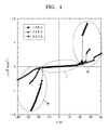
- FIG. 4 is a graph showing the resistance dependence of the current jump of voltage-current density characteristic of a current control circuit including an abrupt metal-insulator phase transition device according to a first embodiment of the present invention.
- a horizontal axis represents a voltage (V) applied between the first electrode 230 and the second electrode 240
- a vertical axis is a current density (J) between the first electrode 230 and the second electrode 240.
- the abrupt metal-insulator phase transition device 200 used in the test of FIG. 4 is a device having the sapphire (Al 2 O 3 ) substrate 210 and the vanadium dioxide (VO 2 ) insulator 220, and has a channel length of 5 ⁇ m between the first electrode 230 and the second electrode 240 and a channel width of 25 ⁇ m.
- Al 2 O 3 the sapphire
- VO 2 vanadium dioxide
- a line indicated by a reference symbol '•' corresponds to a case that the resistance (R) of the resistive element 300 is 1.0 k ⁇
- a line indicated by a reference symbol ' ⁇ ' corresponds to a case that the resistance (R) of the resistive element is 2.5 k ⁇
- a line indicated by a reference symbol ' ⁇ ' corresponds to a case that the resistance (R) of the resistive element 300 is 5.0 k ⁇ .
- FIG. 5 is a graph showing the resistance dependence of the current jump of voltage-current density characteristic of a current control circuit including an abrupt metal-insulator phase transition device according to a second embodiment of the present invention.
- a horizontal axis represents a voltage (V) applied between the first electrode 230 and the second electrode 240
- a vertical axis is a current density (J) between the first electrode 230 and the second electrode 240.
- the abrupt metal-insulator phase transition device 200 used in the test of FIG. 5 is a device using the silicon (Si) substrate 210 and the vanadium dioxide (VO 2 ) insulator 220, and has a channel length of 5 ⁇ m between the first electrode 230 and the second electrode 240 and a channel width of 25 ⁇ m.
- Si silicon
- VO 2 vanadium dioxide
- a line indicated by a reference symbol ' ⁇ ' corresponds to a case that the resistance (R) of the resistive element 300 is 110 ⁇
- a line indicated by a reference symbol '•' corresponds to a case that the resistance (R) of the resistive element 300 is 340 ⁇
- a line indicated by a reference symbol ' ⁇ ' corresponds to a case that the resistance (R) of the resistive element is 1.0 k ⁇
- a line indicated by a reference symbol ' ⁇ ' corresponds to a case that the resistance (R) of the resistive element 300 is 5.0 k ⁇
- a line indicated by a reference symbol ' ⁇ ' corresponds to a case that the resistance (R) of the resistive element 300 is 10 k ⁇ .
- the resistive element connected in series to the abrupt metal-insulator phase transition device suppresses a magnitude of the current jump, so that the abrupt metal-insulator phase transition device can be prevented from being failed and thus the current control circuit can be applied in various application fields.
Landscapes
- Thermistors And Varistors (AREA)
- Semiconductor Memories (AREA)
- Emergency Protection Circuit Devices (AREA)
- Semiconductor Integrated Circuits (AREA)
Abstract
Description
Claims (9)
- A current-jump-control circuit including an abrupt metal-insulator phase transition device, comprising
a source;
the abrupt metal-insulator phase transition device including first and second electrodes connected to the source, and showing an abrupt metal-insulator phase transition characteristic of a current jump when an electric field is applied between the first electrode and the second electrode; and
a resistive element which is connected between the source and the abrupt metal-insulator phase transition device and is able to control a magnitude of a jump current flowing through the abrupt metal-insulator phase transition device. - The current control circuit of claim 1, wherein the resistive element is connected in series with the abrupt metal-insulator phase transition device.
- The current control circuit of claim 1, wherein the resistive element is a resistor.
- The current control circuit of claim 1, wherein the resistive element is an internal resistance material in the inhomogeneous phase-transition thin-film insulator.
- The current control circuit of claim 3, wherein the resistive element is a variable resistor.
- The current control circuit of claim 1, wherein the resistive element is a planar type device pattern that can be used as a resistor.
- The current control circuit of claim 1, wherein the resistive element is an alternating current resistor (or impedance resistance) that can be used as a resistor.
- The current control circuit of claim 1, wherein the abrupt metal-insulator phase transition device has a structure that an insulator film having an abrupt metal-insulator phase transition characteristic of a current jump is disposed between the first electrode and the second electrode.
- The current control circuit of claim 6, wherein the insulator comprises a vanadium oxide.
Applications Claiming Priority (2)
| Application Number | Priority Date | Filing Date | Title |
|---|---|---|---|
| KR2003078333 | 2003-11-06 | ||
| KR1020030078333A KR100576704B1 (en) | 2003-11-06 | 2003-11-06 | Current Control Circuit Including Rapid Metal-Insulator Phase-Transition Device |
Publications (2)
| Publication Number | Publication Date |
|---|---|
| EP1530244A2 true EP1530244A2 (en) | 2005-05-11 |
| EP1530244A3 EP1530244A3 (en) | 2007-05-16 |
Family
ID=34431731
Family Applications (1)
| Application Number | Title | Priority Date | Filing Date |
|---|---|---|---|
| EP04253582A Withdrawn EP1530244A3 (en) | 2003-11-06 | 2004-06-16 | Current-jump-control circuit including abrupt metal-insulator phase transition device |
Country Status (5)
| Country | Link |
|---|---|
| US (1) | US6987290B2 (en) |
| EP (1) | EP1530244A3 (en) |
| JP (1) | JP2005143283A (en) |
| KR (1) | KR100576704B1 (en) |
| CN (1) | CN100337335C (en) |
Cited By (3)
| Publication number | Priority date | Publication date | Assignee | Title |
|---|---|---|---|---|
| EP1911137A4 (en) * | 2005-07-29 | 2011-02-02 | Korea Electronics Telecomm | METAL-INSULATING ABRUPT TRANSITION DEVICE, CIRCUIT USING THE DEVICE FOR REMOVING HIGH VOLTAGE NOISE AND ELECTRICAL AND / OR ELECTRONIC SYSTEM COMPRISING SAID CIRCUIT |
| EP2315288A3 (en) * | 2004-07-15 | 2011-07-06 | Electronics and Telecommunications Research Institute | 2-terminal semiconductor device using abrupt metal-insulator transition semiconductor material |
| EP2036131A4 (en) * | 2006-06-02 | 2013-08-07 | Korea Electronics Telecomm | PROGRAMMABLE METAL-INSULATING TRANSITION SENSOR (MIT) USING THE MIT DEVICE ABRUPTED, AND ALARM APPARATUS AND SECONDARY BATTERY EXPLOSION CIRCUIT COMPRISING THE DETECTOR MITTED |
Families Citing this family (19)
| Publication number | Priority date | Publication date | Assignee | Title |
|---|---|---|---|---|
| JP4143615B2 (en) * | 2005-03-03 | 2008-09-03 | エルピーダメモリ株式会社 | On-die termination circuit |
| KR100714125B1 (en) * | 2005-03-18 | 2007-05-02 | 한국전자통신연구원 | Low voltage noise prevention circuit using abrupt MIT device and electric and electronic system including the circuit |
| KR100809397B1 (en) * | 2005-08-26 | 2008-03-05 | 한국전자통신연구원 | Electron emission device using abruptly metal-insulator transition and display including the same |
| KR100701159B1 (en) * | 2006-02-01 | 2007-03-28 | 한국전자통신연구원 | Metal-insulator transition element with parallel conducting layer structure |
| RU2392692C2 (en) * | 2006-02-01 | 2010-06-20 | Электроникс Энд Телекоммьюникейшнз Рисерч Инститьют | Device with abrupt metal-insulator juction with parallel conducting layers |
| KR100825738B1 (en) * | 2006-03-28 | 2008-04-29 | 한국전자통신연구원 | Voltage control system using abruptly metal-insulator transition |
| KR100825762B1 (en) * | 2006-08-07 | 2008-04-29 | 한국전자통신연구원 | Circuit for measuring a discontinuous metal-insulator transitionMIT continuously and MIT sensor using the same circuit |
| KR100864827B1 (en) * | 2006-11-02 | 2008-10-23 | 한국전자통신연구원 | Logic circuit using metal-insulator transitionMIT device |
| KR100864833B1 (en) | 2006-11-23 | 2008-10-23 | 한국전자통신연구원 | Oscillation circuit based on metal-insulator transitionMIT device and method of driving the same oscillation circuit |
| CN100461485C (en) * | 2007-01-17 | 2009-02-11 | 中国科学院上海微系统与信息技术研究所 | Current limiter based on chalcogenide phase change material and manufacturing method |
| KR100842296B1 (en) | 2007-03-12 | 2008-06-30 | 한국전자통신연구원 | Oscillation circuit based on metal-insulator transition (MITT) element and oscillation frequency control method |
| KR100859717B1 (en) * | 2007-05-07 | 2008-09-23 | 한국전자통신연구원 | 3-terminal MIT switch, switching system using the switch, and MIT control method of the switch |
| KR100901699B1 (en) * | 2007-07-11 | 2009-06-08 | 한국전자통신연구원 | Metal-insulator phase transition memory cell and method of manufacturing the same |
| KR20090049008A (en) | 2007-11-12 | 2009-05-15 | 한국전자통신연구원 | Transistor heating control circuit using metal-insulator transition (MB) element and heating control method thereof |
| US8076662B2 (en) * | 2008-11-26 | 2011-12-13 | President And Fellows Of Harvard College | Electric field induced phase transitions and dynamic tuning of the properties of oxide structures |
| KR101109667B1 (en) | 2008-12-22 | 2012-01-31 | 한국전자통신연구원 | Thermally Enhanced Power Device Package |
| US8362477B2 (en) * | 2010-03-23 | 2013-01-29 | International Business Machines Corporation | High density memory device |
| CN103117538B (en) * | 2013-02-06 | 2015-04-08 | 中国科学院电工研究所 | Resonance type current limiter based on insulator-metal phase change resistor |
| CN112736880A (en) * | 2020-12-25 | 2021-04-30 | 国网浙江省电力有限公司金华供电公司 | Short-circuit current suppression device based on phase change resistor |
Family Cites Families (6)
| Publication number | Priority date | Publication date | Assignee | Title |
|---|---|---|---|---|
| US3588638A (en) * | 1969-05-27 | 1971-06-28 | Energy Conversion Devices Inc | Current controlling device including v02 |
| DE2215878A1 (en) * | 1972-03-30 | 1973-12-06 | Siemens Ag | MAGNETICALLY CONTROLLED SOLID SWITCHING ELEMENT |
| GB2244859A (en) * | 1990-06-04 | 1991-12-11 | Philips Electronic Associated | MIM devices and active matrix displays incorporating such devices |
| US6204139B1 (en) * | 1998-08-25 | 2001-03-20 | University Of Houston | Method for switching the properties of perovskite materials used in thin film resistors |
| US6518609B1 (en) * | 2000-08-31 | 2003-02-11 | University Of Maryland | Niobium or vanadium substituted strontium titanate barrier intermediate a silicon underlayer and a functional metal oxide film |
| KR100433623B1 (en) | 2001-09-17 | 2004-05-31 | 한국전자통신연구원 | Field effect transistor using sharp metal-insulator transition |
-
2003
- 2003-11-06 KR KR1020030078333A patent/KR100576704B1/en not_active Expired - Fee Related
-
2004
- 2004-06-10 US US10/866,274 patent/US6987290B2/en not_active Expired - Lifetime
- 2004-06-16 EP EP04253582A patent/EP1530244A3/en not_active Withdrawn
- 2004-06-28 CN CNB2004100620566A patent/CN100337335C/en not_active Expired - Fee Related
- 2004-08-10 JP JP2004233768A patent/JP2005143283A/en active Pending
Cited By (3)
| Publication number | Priority date | Publication date | Assignee | Title |
|---|---|---|---|---|
| EP2315288A3 (en) * | 2004-07-15 | 2011-07-06 | Electronics and Telecommunications Research Institute | 2-terminal semiconductor device using abrupt metal-insulator transition semiconductor material |
| EP1911137A4 (en) * | 2005-07-29 | 2011-02-02 | Korea Electronics Telecomm | METAL-INSULATING ABRUPT TRANSITION DEVICE, CIRCUIT USING THE DEVICE FOR REMOVING HIGH VOLTAGE NOISE AND ELECTRICAL AND / OR ELECTRONIC SYSTEM COMPRISING SAID CIRCUIT |
| EP2036131A4 (en) * | 2006-06-02 | 2013-08-07 | Korea Electronics Telecomm | PROGRAMMABLE METAL-INSULATING TRANSITION SENSOR (MIT) USING THE MIT DEVICE ABRUPTED, AND ALARM APPARATUS AND SECONDARY BATTERY EXPLOSION CIRCUIT COMPRISING THE DETECTOR MITTED |
Also Published As
| Publication number | Publication date |
|---|---|
| JP2005143283A (en) | 2005-06-02 |
| CN1614786A (en) | 2005-05-11 |
| EP1530244A3 (en) | 2007-05-16 |
| CN100337335C (en) | 2007-09-12 |
| KR100576704B1 (en) | 2006-05-03 |
| US20050098836A1 (en) | 2005-05-12 |
| KR20050043431A (en) | 2005-05-11 |
| US6987290B2 (en) | 2006-01-17 |
Similar Documents
| Publication | Publication Date | Title |
|---|---|---|
| US6987290B2 (en) | Current-jump-control circuit including abrupt metal-insulator phase transition device | |
| US6404269B1 (en) | Low power SOI ESD buffer driver networks having dynamic threshold MOSFETS | |
| EP1678766A1 (en) | Metal-insulator transition switching transistor and method for manufacturing the same | |
| US8536554B2 (en) | Three-terminal metal-insulator transition switch, switching system including the same, and method of controlling metal-insulator transition of the same | |
| KR100467330B1 (en) | Field effect transistor using Vanadium dioxide layer as channel material | |
| US20110006830A1 (en) | High current control circuit including metal-insulator transition device, and system including the high current control circuit | |
| US6646539B2 (en) | Temperature-compensated semiconductor resistor and semiconductor integrated circuit having the semiconductor resistor | |
| CN100536137C (en) | Circuit for protecting electrical and/or electronic system by using abrupt metal-insulator transition device and electrical and/or electronic system comprising the circuit | |
| JP4652434B2 (en) | Variable inductor and electronic circuit device incorporating the same in circuit configuration | |
| US5140299A (en) | Article comprising a high value resistor | |
| US8565001B2 (en) | Method for operating a nonvolatile switching device | |
| RU2392692C2 (en) | Device with abrupt metal-insulator juction with parallel conducting layers | |
| US7199435B2 (en) | Semiconductor devices containing on-chip current sensor and methods for making such devices | |
| JP2583431B2 (en) | Thin-film solid-state equipment | |
| US9048171B2 (en) | Method to dynamically tune precision resistance | |
| US9343206B2 (en) | Electrically-driven phase transitions in functional oxide heterostructures | |
| US12170254B2 (en) | Transistor with integrated short circuit protection | |
| KR100370987B1 (en) | Compound semiconductor device and method for controlling characteristics of the same | |
| Burton | Voltage dependence of activation energy for multilayer ceramic capacitors | |
| KR100701159B1 (en) | Metal-insulator transition element with parallel conducting layer structure | |
| JP7780813B2 (en) | Circuit, varistor device, and method of operating the circuit | |
| US9362419B2 (en) | Variable resistance device having parallel structure | |
| JPH1032105A (en) | Thin film varistor | |
| WO2009014348A2 (en) | Three-terminal metal-insulator transition switch, switching system including the same, and method of controlling metal-insulator transition of the same |
Legal Events
| Date | Code | Title | Description |
|---|---|---|---|
| PUAI | Public reference made under article 153(3) epc to a published international application that has entered the european phase |
Free format text: ORIGINAL CODE: 0009012 |
|
| 17P | Request for examination filed |
Effective date: 20040624 |
|
| AK | Designated contracting states |
Kind code of ref document: A2 Designated state(s): AT BE BG CH CY CZ DE DK EE ES FI FR GB GR HU IE IT LI LU MC NL PL PT RO SE SI SK TR |
|
| AX | Request for extension of the european patent |
Extension state: AL HR LT LV MK |
|
| PUAL | Search report despatched |
Free format text: ORIGINAL CODE: 0009013 |
|
| AK | Designated contracting states |
Kind code of ref document: A3 Designated state(s): AT BE BG CH CY CZ DE DK EE ES FI FR GB GR HU IE IT LI LU MC NL PL PT RO SE SI SK TR |
|
| AX | Request for extension of the european patent |
Extension state: AL HR LT LV MK |
|
| 17Q | First examination report despatched |
Effective date: 20071109 |
|
| AKX | Designation fees paid |
Designated state(s): AT BE BG CH CY CZ DE DK EE ES FI FR GB GR HU IE IT LI LU MC NL PL PT RO SE SI SK TR |
|
| STAA | Information on the status of an ep patent application or granted ep patent |
Free format text: STATUS: THE APPLICATION IS DEEMED TO BE WITHDRAWN |
|
| 18D | Application deemed to be withdrawn |
Effective date: 20100129 |