EP1528663B1 - Vorrichtung zur Steuerung des Leistungsfaktors - Google Patents
Vorrichtung zur Steuerung des Leistungsfaktors Download PDFInfo
- Publication number
- EP1528663B1 EP1528663B1 EP04103438A EP04103438A EP1528663B1 EP 1528663 B1 EP1528663 B1 EP 1528663B1 EP 04103438 A EP04103438 A EP 04103438A EP 04103438 A EP04103438 A EP 04103438A EP 1528663 B1 EP1528663 B1 EP 1528663B1
- Authority
- EP
- European Patent Office
- Prior art keywords
- signal
- voltage
- modules
- main
- digital
- Prior art date
- Legal status (The legal status is an assumption and is not a legal conclusion. Google has not performed a legal analysis and makes no representation as to the accuracy of the status listed.)
- Expired - Lifetime
Links
- 230000001105 regulatory effect Effects 0.000 claims description 3
- 230000005540 biological transmission Effects 0.000 claims description 2
- 238000007599 discharging Methods 0.000 claims 1
- 230000000750 progressive effect Effects 0.000 claims 1
- 230000001960 triggered effect Effects 0.000 claims 1
- 239000003990 capacitor Substances 0.000 description 17
- 230000006870 function Effects 0.000 description 17
- 238000006073 displacement reaction Methods 0.000 description 6
- 238000010586 diagram Methods 0.000 description 5
- 238000000034 method Methods 0.000 description 5
- 230000008901 benefit Effects 0.000 description 4
- 230000001276 controlling effect Effects 0.000 description 4
- 230000008859 change Effects 0.000 description 3
- 235000019800 disodium phosphate Nutrition 0.000 description 2
- 230000000694 effects Effects 0.000 description 2
- 230000010355 oscillation Effects 0.000 description 2
- 239000004065 semiconductor Substances 0.000 description 2
- 230000004913 activation Effects 0.000 description 1
- 238000001914 filtration Methods 0.000 description 1
- 230000008569 process Effects 0.000 description 1
- 238000011084 recovery Methods 0.000 description 1
- 238000005070 sampling Methods 0.000 description 1
- 230000001360 synchronised effect Effects 0.000 description 1
- 230000002123 temporal effect Effects 0.000 description 1
Images


Classifications
-
- H—ELECTRICITY
- H02—GENERATION; CONVERSION OR DISTRIBUTION OF ELECTRIC POWER
- H02M—APPARATUS FOR CONVERSION BETWEEN AC AND AC, BETWEEN AC AND DC, OR BETWEEN DC AND DC, AND FOR USE WITH MAINS OR SIMILAR POWER SUPPLY SYSTEMS; CONVERSION OF DC OR AC INPUT POWER INTO SURGE OUTPUT POWER; CONTROL OR REGULATION THEREOF
- H02M1/00—Details of apparatus for conversion
- H02M1/42—Circuits or arrangements for compensating for or adjusting power factor in converters or inverters
- H02M1/4208—Arrangements for improving power factor of AC input
- H02M1/4225—Arrangements for improving power factor of AC input using a non-isolated boost converter
-
- Y—GENERAL TAGGING OF NEW TECHNOLOGICAL DEVELOPMENTS; GENERAL TAGGING OF CROSS-SECTIONAL TECHNOLOGIES SPANNING OVER SEVERAL SECTIONS OF THE IPC; TECHNICAL SUBJECTS COVERED BY FORMER USPC CROSS-REFERENCE ART COLLECTIONS [XRACs] AND DIGESTS
- Y02—TECHNOLOGIES OR APPLICATIONS FOR MITIGATION OR ADAPTATION AGAINST CLIMATE CHANGE
- Y02B—CLIMATE CHANGE MITIGATION TECHNOLOGIES RELATED TO BUILDINGS, e.g. HOUSING, HOUSE APPLIANCES OR RELATED END-USER APPLICATIONS
- Y02B70/00—Technologies for an efficient end-user side electric power management and consumption
- Y02B70/10—Technologies improving the efficiency by using switched-mode power supplies [SMPS], i.e. efficient power electronics conversion e.g. power factor correction or reduction of losses in power supplies or efficient standby modes
-
- Y—GENERAL TAGGING OF NEW TECHNOLOGICAL DEVELOPMENTS; GENERAL TAGGING OF CROSS-SECTIONAL TECHNOLOGIES SPANNING OVER SEVERAL SECTIONS OF THE IPC; TECHNICAL SUBJECTS COVERED BY FORMER USPC CROSS-REFERENCE ART COLLECTIONS [XRACs] AND DIGESTS
- Y02—TECHNOLOGIES OR APPLICATIONS FOR MITIGATION OR ADAPTATION AGAINST CLIMATE CHANGE
- Y02P—CLIMATE CHANGE MITIGATION TECHNOLOGIES IN THE PRODUCTION OR PROCESSING OF GOODS
- Y02P80/00—Climate change mitigation technologies for sector-wide applications
- Y02P80/10—Efficient use of energy, e.g. using compressed air or pressurized fluid as energy carrier
Definitions
- the present invention relates to a device for controlling the power factor.
- a device for controlling the power factor is disclosed in US 2003/0161167 A1 .
- the "power factor" in an electric load is defined as the ratio between the actual power absorbed by the load itself and the apparent power applied to it.
- the power factor is strictly related to the phase displacement between the current drawn by the load and the voltage applied to the latter by the power source: if the drawn current is completely in phase with and has the same waveform as the applied voltage, the power factor will be equal to 1; if, on the other hand, voltage and current are out of phase and/or have different waveforms, the power factor will be less than 1.
- a power factor with a value of 1 is desirable both from an energy standpoint (energy efficiency is maximised) and for reasons tied to distortion (the voltage waveform will not be substantially distorted by the load).
- the power factor may be much less than 1.
- the above-mentioned circuits are typically provided with a bridge rectifier and an electrolytic capacitor connected to the bus and serving to convert the AC input voltage into an adequately filtered DC voltage.
- correction circuits are installed between the power supply network and the load. These circuits enable a sufficiently high power factor to be obtained (e.g. 0.8-0.9).
- the digital controller measures all the necessary parameters relating to the supply voltage/current and output voltage/current and generates appropriate command signals that are transmitted to the power modules, so that the latter can deliver power to the load while maintaining a high power factor. Furthermore, the digital controller transmits commands to all modules at the same frequency and controls their synchronisation.
- an alternative to the circuits briefly described above may be a completely analog-type circuit.
- the device is of a completely analog type, it is not possible to substantially modify any function without operating directly upon the electronic circuitry, replacing some components or setting them in a particular manner.
- auxiliary control functions relating, for example to overvoltage conditions or, more generally speaking, to situations where the system is not working correctly
- analog implementation of auxiliary control functions is extremely complex, costly and above all offers little flexibility.
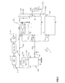
- the number 1 is used to indicate the overall power factor control device according to the present invention.
- Device 1 comprises first of all a rectifier 10, which may be connected to a power supply network 11 in order to receive an AC input voltage 100, preferably of a sinusoidal type, and supply, accordingly, a rectified output voltage 110.
- a rectifier 10 which may be connected to a power supply network 11 in order to receive an AC input voltage 100, preferably of a sinusoidal type, and supply, accordingly, a rectified output voltage 110.
- the AC voltage 100 may be, for example, between 100 and 240 V; advantageously, an EMI (ElectroMagnetic Interference) suppressing filter may be installed between the power supply network 11 and rectifier 10.
- EMI ElectroMagnetic Interference
- Rectifier 10 may be configured as a conventional diode bridge, such as to convert the negative semiwaves of the AC voltage 100 into positive semiwaves and thereby obtain the rectified voltage 110.
- the negative semiwaves of the current drawn from the power supply network 11 will likewise be converted into positive semiwaves to obtain the rectified current I In .
- the rectified voltage 110 and rectified current I in are supplied as input to a first analog module 20 and a second analog module 30.
- the first analog module 20 ( figure 4 ) is provided with an inductor L1, at one end of which is applied the aforesaid rectified voltage 110, connected to a diode D1 in such a way that the latter will allow a flow of current into a capacitor C1, called “bulk capacitor”.
- the drain terminal of a semiconductor device M1 which can be engineered as a MOSFET or an IGBT, is connected between inductor L1 and diode D1; the source terminal of said device is grounded via a resistor R1, generally referred to as "shunt".
- the current flowing across shunt resistor R1 is read by a suitable sensing circuit 591 and input to a current amplifier 601; the latter also receives an input command signal 150, generated by a digital controller that will be described in detail below.
- the two input signals received are compared and the current amplifier 601 generates, accordingly, a signal destined for the above-mentioned command circuit 611, thus closing a feedback loop whose purpose is to regulate the output signal 120 of the first analog module 20.
- the first analog module 20 additionally comprises a first circuit branch 21 and a first resistive divider 24, connected in parallel in order to define the frequency and operating phase of the first module 20 itself.
- the first circuit branch 21 comprises a first resistor 22 having a first end 22a connected to a fixed-potential node and a second end 22b connected to the first end 23a of a first capacitor 23; the second end 23b of the first capacitor 23 is grounded.
- the first resistive divider 24 similarly connected between the aforesaid fixed-potential node and ground, defines at least one level of constant voltage, which lies between the voltage of said fixed-potential node and ground; this constant voltage identifies a first threshold voltage value S1.
- a comparator block 25 has a first input connected to the second end 22b of the first resistor 22 (and thus also to the first end 23a of the first capacitor 23) and a second input connected to the first divider 24; the phase reference of the first output signal 120 is derived by comparing the voltage at the second end 22b of the first resistor 22 and the first threshold value S1.
- a first discharge circuit 26 is connected to the aforesaid first comparator block 25 and to the first capacitor 23, its purpose being to discharge the latter when the voltage at the second end 22b of the first resistor 22 is substantially equal to the first threshold value S1.
- the second analog module 30, also schematically illustrated in figure 4 , has a structure that is wholly similar to the one described above for the first module 20; the second module 30, in fact, comprises an inductor L2, at one end of which is applied the rectified voltage 110, and a diode D2, connected to inductor L2 to induce a flow of current into a bulk capacitor C2.
- a semiconductor device M2 (preferably a MOSFET or IGBT) has a drain terminal connected between inductor L2 and diode D2; the source of device M2 is grounded via a shunt resistor R2.
- the current flowing into resistor R2 is likewise read by a sensing circuit 592 and supplied as input to a current amplifier 602, which compares it with a command signal 150 received from the previously mentioned digital controller; the second output signal 130 delivered by the second analog module 30 is regulated on the basis of this comparison.
- the second module 30 additionally comprises a second circuit branch 31, defined by a second resistor 32 and a second capacitor 33.
- the second resistor 32 has a first end 32a connected to the aforesaid fixed-potential node and a second end 32b connected to the first end 33a of the second capacitor 33; the second end 33b of the second capacitor 33 is grounded.
- the second module 30 is likewise provided with a second resistive divider 34, similarly connected between the fixed-potential node and ground; the second divider 34 thus identifies a second threshold value S2.
- a second comparator block 35 compares the voltage at the second end 32b of the second resistor 32 with the second threshold S2, in order to generate the second output signal 130; in addition, a second discharge circuit 36 discharges the second capacitor 33 when the voltage at the second end 32b of the second resistor 32 is substantially equal to the second threshold S2.
- first and second analog modules 20, 30 are connected in parallel, the first and second output signals 120, 130 will be added together to generate, accordingly, a main signal 140, applied to a load 40; across load 40 there will thus be a main voltage V, while a main current I will flow in load 40 itself.
- the function of device 1 is to ensure that the current drawn from the power supply network 11 has a waveform that is as similar as possible to the waveform of the voltage from network 11, so as to maximise the power factor PF.
- device 1 is provided with a synchronism block 60, which acts upon the first and second analog modules 20, 30 in such a way as to cause a reciprocal phase displacement between said first and second output signals 120, 130.
- the synchronism block 60 delivers a first synchronism signal 160 to the first module 20 and a synchronism signal 170 to the second module 30 in such a way as to ensure that the second output signal 130 will be out of phase with the first output signal 120 by a prefixed amount; since there are two analog modules, this prefixed phase displacement may be conveniently set at 180°.
- module 200 which generates an output signal 201 out of phase of (1/N)*360° with the first output signal 120, another module which generates an output signal 201 out of phase of (2/N)*360° with the first output signal 120, etc., up to a last module whose output signal is ((N-1)/N)*360° out of phase with the first output signal 120.
- the first synchronism signal 160 is preferably defined by the voltage at the second end 22b of the first resistor 22; in other words, the first circuit branch 21 is part of synchronism block 60 and furnishes a reference to the first module 20 for the generation of the first output signal 120.
- the second synchronism signal 170 acts upon the second divider 34 of the second module 30 in such a way as to vary the second threshold value S2 and thereby cause the second output signal 130 to be out of phase with the first output signal 120.
- synchronism block 60 comprises an auxiliary divider 61, which is used to generate an auxiliary threshold value S3; advantageously, auxiliary divider 61 coincides with the aforesaid first divider 24 of the first analog module 20.
- the first divider 24 is thus provided with a first, second and third resistor 27, 28, 29.
- the first resistor 27 has a first end 27a connected to the fixed-potential node and a second end 27b connected to the first end 28a of the second resistor 28; the second end 28b of the latter is connected to the first end 29a of the third resistor 29.
- the second end 29b of the third resistor 29 is grounded.
- the node identified by the second end 27b of the first resistor 27 has a voltage that defines the aforesaid first threshold value S1, whereas the voltage at the second end 28b of the second resistor 28 defines the auxiliary threshold value S3.
- the voltage of the above-mentioned fixed-potential node is divided by means of the first, second and third resistors 27, 28, 29 so as to obtain the aforesaid threshold values S1, S3.
- an auxiliary comparator block 62 compares the auxiliary threshold value S3 with the first synchronism signal 160 in order to generate the aforementioned second synchronism signal 170 based on said comparison and obtain a change in threshold S2 accordingly. The details as regards the generation of these latter signals will become more apparent when reference is made to figure 5 .
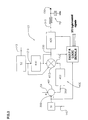
- device 1 In order to control the operation of the aforesaid modules 20, 30 and supply the required power to the load 40 while maintaining the power factor PF at a sufficiently high level, device 1 is equipped with a digital controller 50.
- Digital controller 50 is connected to the above-mentioned rectifier 10 and to the first and second analog module 20, 30 so that it may receive the rectified voltage 110 and main signal 140 as inputs and generate the output command signal 150, to be transmitted to the same modules 20, 30 for the purpose of regulating current I In and thereby controlling both the power factor PF and main voltage V to the load 40.
- digital controller 50 can be an 8-bit microcontroller with 10-bit A/D converter, 2.5Kbyte Program Memory, 256 Bytes RAM, 14 general-purpose I/O and a core of at least 5MIPS.
- controller 50 comprises a first analog-digital converter 51 for measuring the main voltage V across load 40 and obtaining a corresponding first digital signal 300; the latter is essentially a digital representation of the voltage V.
- Controller 50 also comprises a second analog-digital converter 52 for measuring the rectified voltage 110 and obtaining a second digital signal 310; the latter is a digital representation of the value taken on by the rectified voltage 110.
- the first and second digital signals 300, 310 are input to computing means 53, which generate the above-mentioned output command signal 150; in this manner, by suitably operating on modules 20, 30, it is possible to lend current I In a waveform that is substantially identical to the waveform of the rectified voltage 110, so as to optimise the power factor PF.
- the main voltage V is maintained at a constant level regardless of the power demanded by the load 40.
- the computing means 53 are equipped with a comparator block 400, which receives the first digital input signal 300 and compares it with a pre-memorised threshold S4 to obtain an error signal 320.
- comparator block 400 consists of a differentiating circuit 401 for determining the difference between the first digital signal 300 and the pre-memorised threshold S4; in practical terms, the difference between the value taken on by the main voltage V, numerically represented by the first digital signal 300, and the threshold S4 is determined instant by instant so as to obtain a corresponding difference signal 360, which will be used in the computations described below.
- the first digital signal 300 before being compared with threshold S4, can be advantageously filtered and amplified so as to obtain a corresponding secondary signal 300a.
- the difference signal 360 is input to an auxiliary filter 402, connected downstream to said differentiating circuit 401.
- Auxiliary filter 402 comprises integrating means 402a, which receive the difference signal 360 and output a first computed signal 370, which is proportional to an integral of the difference signal 360 itself, calculated in relation to time; the integrating means 402a can be obtained, in practice, by connecting an integrator in series with an amplifier; the latter will define the proportionality parameter by which to multiply the result of the integral in order to obtain the first computed signal 370.
- Auxiliary filter 402 further comprises an amplifier 402b, which is likewise configured to receive the difference signal 360 as an input; the output of amplifier 402b consists in a second computed signal 380, directly proportional to the difference signal 360 based on a parameter defined by amplifier 402b itself.
- Auxiliary filter 402 also comprises an addition circuit 402c, which receives the first and second computed signals 370, 380 as inputs and adds them together; the resulting sum is the error signal 320.
- the computing means 53 further comprise a multiplier block 410; it receives as inputs the error signal 320, the second digital signal 310 and a third digital signal 350 (which will be described below) and multiplies them to generate an output signal 330 corresponding to the result of the multiplication.
- the third digital signal 350 is generated by a main filter 430 from the second digital signal 310; the third digital signal 350 numerically represents the reciprocal of the square of the average quadratic value of the rectified voltage 110 represented by the second digital signal 310.
- the third digital signal 350 is calculated by referring to a pre-memorised look-up table which gives the most probable values for the rectified voltage 110, along with the respective results, rather than relying on continuous real-time calculations of the reciprocal of the square of the number represented by the second digital signal 310.
- the additional use of the third multiplicative factor defined by the third digital signal 350 makes it possible to compensate for any rapid fluctuations in the supply voltage 100 without affecting the operation of the system as a whole.
- multiplier block 410 is represented with two distinct multiplier nodes 410a, 410b to better illustrate the process by which the resulting signal 330 is generated (and power is accordingly delivered to the load 40).
- each node 410a, 410b The functional characteristics of each node 410a, 410b will become apparent from the description of the operation of device 1.
- the resulting signal 330 is input to modulation means 420 which, based on signal 330 itself, output a sequence of pulses defining a square wave signal 340; more particularly, all the pulses have the same amplitude, but their duration will vary according to the information incorporated in the resulting signal 330.
- the modulation means 420 consist of a PWM-type modulator.
- the square wave 340 is input to an integrator block 70, connected to computing means 53, and in particular to the aforesaid modulation means 420; the integrator block 70, advantageously engineered with one or more resistors and one or more capacitors connected as shown in figure 3 , generates the above-mentioned command signal 150 on the basis of square wave 340.
- Command signal 150 is thus obtained by integrating square wave 340 generated by PWM 420; therefore, command signal 150 has an amplitude proportional to the duty cycle of square wave 340 itself.
- device 1 In order to ensure the correct functioning of device 1 and any other equipment connected thereto, device 1 itself is endowed with a first control circuit 440.
- the first control circuit 440 comprises comparator means 441 that compare the first digital signal 300 with a first auxiliary threshold S5, which represents a working limit for device 1; i.e. the first auxiliary threshold S5 indicates a maximum value for the main voltage V, a limit that must not be surpassed to prevent system faults or malfunctioning.
- shutdown means 442 will intervene to shut down the analog modules 20, 30 and thus cut off the supply of power to the load 40, as a problem is likely to have occurred within the circuit; furthermore, again in the event that the main voltage V, represented by the first digital signal 300, exceeds the first auxiliary threshold S5, discharge means 443 will at least partly discharge the integrating means 402a of auxiliary filter 402.
- Said discharge which may fixed, for example, at 12.5% of the total charge, advantageously enables a faster recovery from the overvoltage situation, i.e. it permits the normal operating conditions of device 1 to be restored more quickly.
- the shutting down of modules 20, 30 by shutdown means 442 can be achieved by forcing the duty cycle of PWM 420 to zero.
- the control function provided by the aforesaid first circuit 440 is a software-based control function performed by controller 50 according to numbers received as inputs in a digital format.
- the computing means 53 will comprise a second control circuit 450 serving to provide control over the main voltage V.
- the second control circuit 450 is provided with comparator means 451 whose function is to compare the main voltage V with a second auxiliary threshold S6 and to determine in particular whether the main voltage V is lower than said threshold; if such is the case, a correction block 452 will intervene to increase the first proportionality parameter of the aforesaid integrating means 402a and/or the second proportionality parameter of the aforesaid amplifier 402b, according to the difference between the main voltage V and second auxiliary threshold S6.
- control function of the second circuit 450 may be performed directly on the first digital signal 300, representing the main voltage V, or, in a wholly equivalent manner, on the difference signal 360 generated by the differentiating circuit 401; needless to say, in each of these two cases the second auxiliary threshold S6 must be set accordingly.
- This control function is useful in that it enables the normal operating conditions of device 1 to be restored more quickly after a voltage drop below the preset limit.
- An additional control function is performed by a third control circuit 80, of the analog type, comprising comparator means 81 whose function is to compare the main voltage V with a third auxiliary threshold S7 (advantageously selected so as to be greater than or equal to the first auxiliary threshold S5) and a command block 82 for shutting down the first and second modules 20, 30 in the event that the main voltage V exceeds the third threshold S7.
- a transmission block 83 is connected to the comparator means 81 so that an alarm signal 390 may be sent to the computing means 53 in the event that the main voltage V exceeds the third threshold S7.
- the computing means 53 are thus equipped with receiving means 460 for receiving the alarm signal 390 and a restart block 461, whose function is to make a preset number of attempts to restart the analog modules 20, 30 previously shut down by the above-mentioned command means 82; an event counter 700 keeps track of the number of attempts made and on reaching a certain limit (e.g. 8 attempts) causes modules 20, 30 to shut down permanently. At this point, in order to re-enable their operation it will be necessary to disconnect the system from the power supply for a preset time interval and then reconnect it to the power supply.
- a certain limit e.g. 8 attempts
- the third control circuit 80 carries out a hardware check on the value of the main voltage V; being an analog-type function, the check can take place even if controller 50 breaks down and interrupts its computing activity.
- the current reference generated by controller 50 is short circuited to earth, thus preventing analog modules 20, 30 from receiving the command signal 150 and, consequently, from supplying power to the load 40.
- device 1 is also equipped with an auxiliary power unit 500; the latter receives the main input voltage V and outputs a first supply voltage 501 (e.g. 3 or 5 V) for the digital controller 50 and a second supply voltage Vcc (for example 12V) destined for analog modules 20, 30, also used to define the voltage of the above-mentioned fixed-potential node to which circuit branches 21, 31 and dividers 24, 34 are connected.
- a first supply voltage 501 e.g. 3 or 5 V
- Vcc for example 12V
- controller 50 may be provided with an I/O interface for the exchange of data with equipment external to device 1, for example for the purpose of running further checks on the operating conditions of the system in which device 1 is installed.
- controller 50 It is important to emphasise, with regard to controller 50, that the various functional blocks described above are mere representations of the functions of controller 50 itself and do not identify concrete circuit blocks physically present in device 1; in other words, the aforesaid blocks (schematically illustrated in figure 3 ) serve to illustrate how the software loaded in controller 50 enables the latter to work.
- the rectified voltage 110 is supplied directly to load 40 itself through inductors L1, L2 and diodes D1, D2, given that the power factor (PF) control activity has not yet started and devices M1, M2 are disabled.
- the main voltage V which at this point is essentially equal to the peak of the rectified voltage 110, is brought back to controller 50, which activates the regulation procedures.
- the main voltage V expressed via the first digital signal 300 and filtered by a digital filter 470, is compared with reference S4 and error signal 320 is obtained by means of the functional blocks described above; it may be noted that functional blocks 401, 402, 470 define a system for controlling the main voltage V.
- the passband of the system for controlling the voltage V should not exceed 10Hz.
- the main voltage V is sampled here at a frequency of 1.2 - 1.5KHz; in fact, as is well known, the oversampling of a limited-band signal, followed by digital filtering, allows an increase in resolution of 1/2 bit for every doubling of the sampling frequency.
- the rectified voltage 110 is simultaneously sampled at a frequency of about 20KHz to obtain the second digital signal 310; the third digital signal 350 is derived from the latter, through the main filter 430 described above, and is multiplied with the error signal 320 from the first multiplier node 410a.
- the output of the first multiplier node 410a is compared instant by instant with a ramp generated by generator 510; switch 520 is thus controlled on the basis of said comparison. More particularly, whenever the value of the ramp proves to be lower than the output of the first node 410a, the switch is placed in a first condition in which it connects the output of the ramp generator 510 with the second multiplier node 410b; whenever the value of the ramp exceeds the first multiplier node 410a, switch 520 is placed in a second condition in which it connects the output of the first multiplier node 410a with an input of the second multiplier node 410b.
- the second multiplier node 410b then multiplies the second digital signal 310 and the signal selected by switch 520 to obtain the resulting signal 330.
- the resulting signal 330 is defined, unless a proportionality factor is introduced, as the product of the main voltage V, rectified voltage 110 and reciprocal of the square of the average value of the rectified voltage 110.
- the resulting signal 330 causes the modulation means 420 to generate a square wave 340, preferably according to the PWM technique; in particular, in light of the above description, it is evident that if the value of the main voltage V is very far from the reference value represented by threshold S4, the duty cycle of the PWM will be very great. If, on the contrary, the value of the main voltage V is fairly close to the preset threshold, the duty cycle of the PWM will be smaller.
- the second digital signal 310 (i.e. the digital representation of the rectified voltage 110) fed to the input of multiplier block 410 makes it possible to precisely define the waveform that must be assumed by current I In ; in fact, since the above-mentioned input current I In and rectified voltage 110 are required to have the same waveform, the presence of a substantially resistive load is simulated downstream from rectifier 10, which brings the power factor PF to values approaching one.
- Square wave 340 is converted into command signal 150 by integrator block 70; command signal 150 is an analog signal whose amplitude is proportional to the area defined by the pulses of square wave 340. In other words, the amplitude of command signal 150 is proportional to the duty cycle of square wave 340.
- command signal is transmitted to analog modules 20, 30.
- command signal 150 is received by current amplifier 601; the latter compares command signal 150 (which represents the optimal current) with the current measured by circuit 591.
- an appropriate signal is sent to the command circuit 611; the latter in turn generates a signal 621 that activates device M1 according to the PWM technique, with a variable duty cycle such as to cancel out the difference between the current set by the command signal 150 and the current measured by circuit 591.
- Command circuit 611 can also generate the first synchronism signal 160 and receives the first threshold value S1.
- the first capacitor 23 is charged via the first resistor 21, as the latter is connected to the fixed-potential node Vdc.
- the first comparator block 25 switches on the first discharge block 26, which rapidly discharges the first capacitor 23.
- the first synchronism signal 160 displays a sawtooth pattern as illustrated in figure 5 .
- the first synchronism signal 160 that can be generated by command circuit 611 defines the frequency of oscillation of the PWM included in said command circuit 611, which in turn identifies the frequency with which device M1 is turned on and off for the regulation of the first output signal 120.
- the second analog module 30 functions in a wholly identical manner; the only difference lies in the method by which the second threshold S2 is defined.
- the second circuit branch 31 and second divider 34, together with the second comparator block 35 and second discharge circuit 36, generate a sawtooth-patterned signal 171 that is similar in every respect to the first synchronism signal 160.
- the second threshold S2 is fixed via synchronism block 60, and specifically by means of auxiliary comparator block 62, in such a manner as to introduce a preset phase lag between the first output signal 120 and the second output signal 130.
- the auxiliary comparator block 62 compares the first synchronism signal 160 with the auxiliary threshold value S3 defined by auxiliary divider 61; when the first synchronism signal 160 is essentially equal to said threshold S3, the second threshold S2 is lowered accordingly and the second capacitor 33 is discharged, determining the start of a new period in the sawtooth wave of auxiliary signal 171, which is the signal that defines the oscillation frequency and phase displacement in relation to the first synchronism signal 160 of the PWM incorporated in the aforesaid second command circuit 612.
- Figure 5 schematically illustrates how the second threshold S2 is lowered and auxiliary signal 171 is accordingly brought to a value of zero when the synchronism signal 160 reaches the value S3.
- the lowering of the second threshold S2, caused by the second synchronism signal 170, will preferably be proportional at least to the difference between the frequency of first synchronism signal 160 and the initial frequency defined by components 32, 33 of the second analog module 30.
- the optimal phase difference between the first and second output signal 120, 130 is equal to 180°
- auxiliary divider 61 In configurations with more than two power modules, the auxiliary divider 61 would obviously be provided with a larger number of resistors connected in series; more specifically, auxiliary divider 61 comprises a number of resistors equal to N+1, where N is the total number of modules. Via N+1 resistors it is in fact possible to identify N reference thresholds, to be used to define the phase displacements between the various output signals.
- the operating frequency of the second analog module 30 (and any other modules 200) controlled by components 32 and 33 is initially slightly less (by about 10%) than the operating frequency of the first module 20; this permits the second module 30 to be correctly synchronised by module 20 and thereafter brought to the same working frequency.
- the invention provides some important advantages.
- the device according to the invention can be used to correct the power factor of a load and control a plurality of analog power modules in an economical, flexible and dynamic manner.
- the device according to the invention features a plurality of control functions, which enable the device itself to operate in a precise and reliable manner even in the event of abrupt variations in the supply voltage or in the entity of the load.
- the main voltage V is maintained at a constant level with good accuracy and precision during operation of the device; said main voltage V is also fixed in a significantly uniform manner in several distinct devices configured as described above.
- control circuits make it possible to limit the number of system restart attempts in case of a serious fault, triggering a permanent system shutdown.
Landscapes
- Engineering & Computer Science (AREA)
- Power Engineering (AREA)
- Rectifiers (AREA)
- Control Of Eletrric Generators (AREA)
- General Induction Heating (AREA)
- Control Of Motors That Do Not Use Commutators (AREA)
Claims (7)
- Vorrichtung zur Steuerung des Leistungsfaktors, umfassend;- einen Gleichrichter (10), der mit einem Wechselstromnetz (1) verbindbar ist, um am Eingang eine Wechselspannung (100) zu empfangen und am Ausgang eine gleichgerichtete Spannung (110) zu liefern;- einen ersten Analogmodul (20), der mit dem Gleichrichter (10) verbunden ist, um die gleichgerichtete Spannung (110) zu empfangen und ein entsprechendes Ausgangssignal (120) zu erzeugen;- einen zweiten Analogmodul (130), der mit dem ersten Analogmodul (20) parallel geschaltet und mit dem Gleichrichter (10) verbunden ist, um die gleichgerichtete Spannung (110) zu empfangen und ein entsprechendes, zweites Ausgangssignal (130) zu erzeugen, wobei das erste und das zweite Ausgangssignal (120, 130) zusammenwirken, um ein Hauptsignal (140) zu erhalten, das für eine Last (40) bestimmt ist und eine Hauptspannung (V) der Last (40) und einen vom Gleichrichter (10) abgegebenen Eingangsstrom (IIn) abgegebenen Eingangsstrom festlegt, dadurch gekennzeichnet, dass sie überdies umfasst:wobei der Vergleichsblock (400) umfasst:- einen Digitalkontroller (50), der mit dem Gleichrichter (10) und mit dem ersten und dem zweiten Analogmodul (20, 30) verbunden ist, um am Eingang die gleichgerichtete Spannung (110) und das Hauptsignal (140) zu empfangen und um ein entsprechendes Steuersignal (150) zu erzeugen, das für den ersten und den zweiten Analogmodul (20, 30) bestimmt ist, um mindestens den Eingangsstrom (IIn) einzustellen und eine entsprechende Steuerung eines Leistungsfaktors (PF) der Last (40) zu erhalten,- einen ersten Analog-Digital-Umsetzer (51), um die Hauptspannung (V) zu erfassen und ein entsprechendes erstes digitales Signal (30) zu erhalten, das die Hauptspannung (V) darstellt;- einen zweiten Analog-Digital-Umsetzer (52), um die gleichgerichtete Spannung (110) zu erfassen und ein entsprechendes zweites Digital-Signal (310) zu erhalten, das die gleichgerichtete Spannung (110) darstellt;- Verarbeitungsmittel (53), um das erste und das zweite Digitalsignal (30, 310) zu empfangen und am Ausgang das Steuersignal (150) zu liefern, um dem Eingangsstrom (IIn) eine im wesentlichen einer Wellenform der gleichgerichteten Spannung (110) gleiche Wellenform und eine Amplitude zu erteilen, die Funktion der Hauptspannung (V) ist, wobei die Verarbeitungsmittel (53 umfassen:- einen Vergleichsblock (400), um das erste Digitalsignal (300) mit einer vorgespeicherten Schwelle (S4) zu vergleichen und ein entsprechendes Fehlersignal (320) zu erhalten;- einen Multiplizierblock (410), um das Fehlersignal (320) und das zweite Digitalsignal (310) miteinander zu multiplizieren und ein entsprechendes Resultatsignal (330) zu erhalten;- Moduliermittel (420), die mit dem Multiplizierblock (410) verbunden sind, um das Resultatsignal (330) zu empfangen und am Ausgang eine Impulsfolge zu erzeugen, die ein quadratwellenförmiges Signal (340) festlegt, das jeweils eine Zeitdauer besitzt, die Funktion des Resultatsignals (330) ist,- eine Differenzierschaltung (401), um eine Differenz zwischen dem ersten Digitalsignal (300) und der vorgespeicherten Schwelle (S4) durchzuführen, wobei ein entsprechendes Differenzsignal (360) erhalten wird;- ein Hilfsfilter (402), das zwischen der Differenzschaltung (401) und dem Multiplizierblock (410) zwischengeschaltet und versehen ist mit:• Integriermitteln (402a), um das Differenziersignal (360) zu empfangen und ein entsprechendes erstes Verarbeitungssignal (370) zu erzeugen, das gemäß einem ersten Proportionalitätsparameter zu einem Integral des ersten Differenzsignals (360) proportional ist;• einem Verstärker (402b), um das Differenzsignal (360) zu empfangen und ein entsprechendes zweites Verarbeitungssignal (380) zu erzeugen, das gemäß einem zweiten Proportionalitätsparameter zum Differenzsignal (360) proportional ist;• einer Summierschaltung (402c), um das erste und das zweite Verarbeitungssignal (370, 380) miteinander zu summieren und das Fehlersignal (320) zu erhalten,wobei die Verarbeitungsmittel (53) überdies eine zweite Steuerschaltung (450) umfassen, die versehen ist mit:- Vergleichsmitteln (451), um zu überprüfen, ob die Hauptspannung (V) größer als eine zweite Hilfswelle (S6) ist;- einem Korrekturblock (452), der auf die Integriermittel (402) und den Verstärker (402b) des Hilfsfilters (402) wirkt, um den ersten und/oder zweiten Proportionalitätsparameter in Abhängigkeit einer Differenz zwischen der Hauptspannung (V) und der zweiten Hilfsschwelle (S6) zu erhöhen.
- Vorrichtung nach Anspruch 1, dadurch gekennzeichnet, dass sie überdies eine Vielzahl von Analogmodulen (200) umfasst, die zueinander parallel geschaltet sind, wobei jeder der Module mit dem Gleichrichter (10) verbunden ist, um am Eingang die gleichgerichtete Spannung (110) zu empfangen und ein entsprechendes Ausgangssignal (201) zu erzeugen, wobei die Ausgangssignale (201) zusammenwirken, um das Hauptsignal (140) zu erhalten, wobei jedes der Ausgangssignale (201) bevorzugter Weise gegenüber dem ersten Ausgangssignal (120) um eine zur Anzahl der Module (200) umgekehrt proportionale Größe bevorzugter Weise fasenverschoben ist, und insbesondere gleich ist zu:
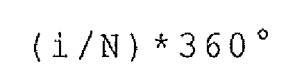
wobei "N" die Anzahl der Analogmodule (200) und "i" ein zunehmendes Ganzes ist, das eindeutig der Reihenfolge nach jenes der Analogmodule (200) bestimmt. - Vorrichtung nach Anspruch 1, dadurch gekennzeichnet, dass sie überdies einen Integrierblock (20) umfasst, der mit den Verarbeitungsmitteln (53) verbunden ist, um das quadratwellenförmige Signal (340) zu empfangen und am Ausgang das Steuersignal (150) zu erzeugen.
- Vorrichtung nach Anspruch 1, dadurch gekennzeichnet, dass die Verarbeitungsmittel (53) überdies ein Hauptfilter (430)umfassen, um am Eingang das Digitalsignal (310) zu empfangen und am Ausgang ein drittes Digitalsignal (350) zu erzeugen, das eine Reziprokzahl des Quadrates eines Mittelwertes der gleichgerichteten Spannung (110) darstellt und für den Multiplizierblock (410) bestimmt ist, wobei das Resultatsignal (330) durch ein Produkt zwischen dem ersten Digitalsignal (310) dem Fehlersignal (320) und dem dritten Digitalsignal (350) erhalten ist.
- Vorrichtung nach Anspruch 1, dadurch gekennzeichnet, dass die Verarbeitungsmittel (53) überdies eine erste Steuerschaltung (440) umfassen, die versehen ist mit:- Vergleichsmittel (441), um zu überprüfen, ob das erste Digitalsignal (300) größer ist als eine erste Hilfsschwelle (S5);- Deaktivierungsmittel (442), um die Analogmodule (20, 30) zu deaktivieren;- Entlademittel (443), um mindestens teilweise die Integriermittel (402a) des Hilfsfilters (402) zu entladen.
- Vorrichtung nach Anspruch 1, dadurch gekennzeichnet, dass sie überdies eine dritte Steuerschaltung (80) umfasst, die versehen ist mit:- Vergleichsmitteln (81), um die Hauptspannung (V) mit einer dritten Hilfsschwelle (S7) zu vergleichen, wobei diese letztere bevorzugter Weise größer oder gleich der ersten Hilfsschwelle (S5) ist;- einem Steuerblock (82), der mit den Vergleichsmitteln (81) verbunden ist, um den ersten und den zweiten Analogmodul (20, 30) zu deaktivieren, wenn die Hauptspannung (V) größer ist als die dritte Hilfsschwelle (S7);- einem Sendeblock (83), der mit den Vergleichsmitteln (81) verbunden ist, um den Verarbeitungsmitteln (51) ein Alarmsignal (390) im Fall zu senden, bei dem die Hauptspannung (V) größer ist als die dritte Hilfsschwelle (S7).
- Vorrichtung nach Anspruch 6, dadurch gekennzeichnet, dass die Verarbeitungsmittel (53) überdies umfassen:- Empfangsmittel (460), um das Alarmsignal (390) zu empfangen;- einen Neustartblock (461), um für eine vorgegebene Anzahl von Malen zu versuchen, die Analogmodule (20, 30) zufolge der durch die Steuermittel (83) hervorgerufene Deaktivierung zu aktivieren.
Applications Claiming Priority (2)
| Application Number | Priority Date | Filing Date | Title |
|---|---|---|---|
| IT002095A ITMI20032095A1 (it) | 2003-10-28 | 2003-10-28 | Dispositivo per il controllo del fattore di potenza. |
| ITMI20032095 | 2003-10-28 |
Publications (3)
| Publication Number | Publication Date |
|---|---|
| EP1528663A2 EP1528663A2 (de) | 2005-05-04 |
| EP1528663A3 EP1528663A3 (de) | 2005-08-31 |
| EP1528663B1 true EP1528663B1 (de) | 2009-01-07 |
Family
ID=34401311
Family Applications (1)
| Application Number | Title | Priority Date | Filing Date |
|---|---|---|---|
| EP04103438A Expired - Lifetime EP1528663B1 (de) | 2003-10-28 | 2004-07-19 | Vorrichtung zur Steuerung des Leistungsfaktors |
Country Status (5)
| Country | Link |
|---|---|
| US (1) | US6975524B2 (de) |
| EP (1) | EP1528663B1 (de) |
| AT (1) | ATE420488T1 (de) |
| DE (1) | DE602004018888D1 (de) |
| IT (1) | ITMI20032095A1 (de) |
Families Citing this family (7)
| Publication number | Priority date | Publication date | Assignee | Title |
|---|---|---|---|---|
| US7411378B2 (en) * | 2004-05-07 | 2008-08-12 | Embed, Inc. | Power factor controller that computes currents without measuring them |
| US7385372B2 (en) | 2004-05-27 | 2008-06-10 | Siemens Energy & Automation, Inc. | Auxiliary bus system |
| US7323851B2 (en) * | 2005-09-22 | 2008-01-29 | Artesyn Technologies, Inc. | Digital power factor correction controller and AC-to-DC power supply including same |
| WO2010126491A1 (en) * | 2009-04-28 | 2010-11-04 | Semiconductor Components Industries, Llc | Method for providing over current protection and circuit |
| US8098506B2 (en) | 2009-06-02 | 2012-01-17 | Power Integrations, Inc. | Single-stage power supply with power factor correction and constant current output |
| JP4844696B2 (ja) * | 2010-03-26 | 2011-12-28 | ダイキン工業株式会社 | スイッチング電源回路およびスイッチング電源回路の制御方法 |
| JP5739622B2 (ja) * | 2010-06-03 | 2015-06-24 | スパンション エルエルシー | 半導体集積回路、半導体集積回路の動作方法およびデバッグシステム |
Citations (1)
| Publication number | Priority date | Publication date | Assignee | Title |
|---|---|---|---|---|
| US20020011845A1 (en) * | 2000-06-15 | 2002-01-31 | Van Den Brink Johan Samuel | Magnetic resonance imaging method involving sub-sampling |
Family Cites Families (11)
| Publication number | Priority date | Publication date | Assignee | Title |
|---|---|---|---|---|
| US4677366A (en) | 1986-05-12 | 1987-06-30 | Pioneer Research, Inc. | Unity power factor power supply |
| US5088019A (en) | 1990-09-18 | 1992-02-11 | Hewlett-Packard Company | Low harmonic current and fault tolerant power supply |
| US5103388A (en) | 1990-09-18 | 1992-04-07 | Hewlett-Packard Company | Low harmonic current and fault tolerant power supply |
| US5359276A (en) | 1993-05-12 | 1994-10-25 | Unitrode Corporation | Automatic gain selection for high power factor |
| US5631550A (en) | 1996-04-25 | 1997-05-20 | Lockheed Martin Tactical Defense Systems | Digital control for active power factor correction |
| GB9608832D0 (en) * | 1996-04-30 | 1996-07-03 | Switched Reluctance Drives Ltd | Power factor correction circuit |
| EP0951133A3 (de) * | 1998-04-15 | 2000-04-12 | HILTI Aktiengesellschaft | Verfahren und aktives Filter zur Reduzierung der Restwelligkeit des einem Netz durch eine Last entnommenen Stroms |
| US6621253B2 (en) * | 2001-09-20 | 2003-09-16 | Gibson Guitar Corp. | Amplifier having a variable power factor |
| US6690589B2 (en) * | 2002-02-28 | 2004-02-10 | Valere Power, Inc. | Interleaved converter power factor correction method and apparatus |
| US6650092B1 (en) * | 2002-05-24 | 2003-11-18 | Motorola, Inc. | System and method for regulating a power system with feedback using current sensing |
| US6903946B1 (en) * | 2003-11-04 | 2005-06-07 | Lockheed Martin Corporation | Paralleled power factor correcting AC-to-DC converters with improved current balance |
-
2003
- 2003-10-28 IT IT002095A patent/ITMI20032095A1/it unknown
-
2004
- 2004-07-19 DE DE602004018888T patent/DE602004018888D1/de not_active Expired - Fee Related
- 2004-07-19 EP EP04103438A patent/EP1528663B1/de not_active Expired - Lifetime
- 2004-07-19 AT AT04103438T patent/ATE420488T1/de not_active IP Right Cessation
- 2004-09-09 US US10/937,050 patent/US6975524B2/en not_active Expired - Fee Related
Patent Citations (1)
| Publication number | Priority date | Publication date | Assignee | Title |
|---|---|---|---|---|
| US20020011845A1 (en) * | 2000-06-15 | 2002-01-31 | Van Den Brink Johan Samuel | Magnetic resonance imaging method involving sub-sampling |
Also Published As
| Publication number | Publication date |
|---|---|
| ATE420488T1 (de) | 2009-01-15 |
| US6975524B2 (en) | 2005-12-13 |
| EP1528663A2 (de) | 2005-05-04 |
| ITMI20032095A1 (it) | 2005-04-29 |
| EP1528663A3 (de) | 2005-08-31 |
| US20050088864A1 (en) | 2005-04-28 |
| DE602004018888D1 (de) | 2009-02-26 |
Similar Documents
| Publication | Publication Date | Title |
|---|---|---|
| US5631550A (en) | Digital control for active power factor correction | |
| US6728121B2 (en) | Method and apparatus for active power factor correction with minimum input current distortion | |
| CN205657593U (zh) | 开关稳压器和电子设备 | |
| US7447601B2 (en) | Power supply controller method and structure | |
| US5115185A (en) | Single conversion power factor correction using septic converter | |
| US9762130B2 (en) | Switching controller for switching power supply | |
| EP2104217A2 (de) | Motorsteuerung | |
| US7394232B2 (en) | Interleaved switching converters in ring configuration | |
| WO1993026078A1 (en) | High power factor switched dc power supply | |
| WO1996007960A1 (en) | A synchronous switching cascade connected offline pfc-pwm combination power converter controller | |
| US12294295B2 (en) | Systems and methods of unwanted harmonic content removal for power conversion | |
| US20220166307A1 (en) | Electrical circuits for power factor correction by measurement and removal of overtones and power factor maximization | |
| JPH01283063A (ja) | Pwm制御による電源装置 | |
| EP1528663B1 (de) | Vorrichtung zur Steuerung des Leistungsfaktors | |
| JP4207824B2 (ja) | スイッチング電源装置 | |
| US11552554B2 (en) | Electrical circuits for power factor correction by measurement and removal of overtones using a constant or slowly varying first frequency | |
| JP2001190073A (ja) | 力率補正電気変換装置 | |
| US7102341B1 (en) | Apparatus for controlling a power factor correction converter device | |
| US8472211B2 (en) | Single stage power conversion unit with circuit to smooth and holdup DC output voltage | |
| CN113938019A (zh) | 电源电路与电子设备 | |
| CN220935031U (zh) | 直流高压逆变装置 | |
| CN214674941U (zh) | 电源转换器及其限流控制电路 | |
| JPH05333077A (ja) | スイッチング型模擬負荷装置 | |
| Diwan et al. | Proposed topology for voltage sag mitigation with new control strategy | |
| SU784032A1 (ru) | Рентгеновский генератор |
Legal Events
| Date | Code | Title | Description |
|---|---|---|---|
| PUAI | Public reference made under article 153(3) epc to a published international application that has entered the european phase |
Free format text: ORIGINAL CODE: 0009012 |
|
| AK | Designated contracting states |
Kind code of ref document: A2 Designated state(s): AT BE BG CH CY CZ DE DK EE ES FI FR GB GR HU IE IT LI LU MC NL PL PT RO SE SI SK TR |
|
| AX | Request for extension of the european patent |
Extension state: AL HR LT LV MK |
|
| PUAL | Search report despatched |
Free format text: ORIGINAL CODE: 0009013 |
|
| AK | Designated contracting states |
Kind code of ref document: A3 Designated state(s): AT BE BG CH CY CZ DE DK EE ES FI FR GB GR HU IE IT LI LU MC NL PL PT RO SE SI SK TR |
|
| AX | Request for extension of the european patent |
Extension state: AL HR LT LV MK |
|
| 17P | Request for examination filed |
Effective date: 20051212 |
|
| AKX | Designation fees paid |
Designated state(s): AT BE BG CH CY CZ DE DK EE ES FI FR GB GR HU IE IT LI LU MC NL PL PT RO SE SI SK TR |
|
| 17Q | First examination report despatched |
Effective date: 20060120 |
|
| GRAP | Despatch of communication of intention to grant a patent |
Free format text: ORIGINAL CODE: EPIDOSNIGR1 |
|
| RIN1 | Information on inventor provided before grant (corrected) |
Inventor name: SABBATINI, DANIELE Inventor name: NICOLINI, ANGELO Inventor name: MONTORSI, FRANCESCO |
|
| GRAS | Grant fee paid |
Free format text: ORIGINAL CODE: EPIDOSNIGR3 |
|
| GRAA | (expected) grant |
Free format text: ORIGINAL CODE: 0009210 |
|
| AK | Designated contracting states |
Kind code of ref document: B1 Designated state(s): AT BE BG CH CY CZ DE DK EE ES FI FR GB GR HU IE IT LI LU MC NL PL PT RO SE SI SK TR |
|
| REG | Reference to a national code |
Ref country code: GB Ref legal event code: FG4D |
|
| REG | Reference to a national code |
Ref country code: CH Ref legal event code: EP |
|
| REG | Reference to a national code |
Ref country code: IE Ref legal event code: FG4D |
|
| REF | Corresponds to: |
Ref document number: 602004018888 Country of ref document: DE Date of ref document: 20090226 Kind code of ref document: P |
|
| PG25 | Lapsed in a contracting state [announced via postgrant information from national office to epo] |
Ref country code: SI Free format text: LAPSE BECAUSE OF FAILURE TO SUBMIT A TRANSLATION OF THE DESCRIPTION OR TO PAY THE FEE WITHIN THE PRESCRIBED TIME-LIMIT Effective date: 20090107 Ref country code: NL Free format text: LAPSE BECAUSE OF FAILURE TO SUBMIT A TRANSLATION OF THE DESCRIPTION OR TO PAY THE FEE WITHIN THE PRESCRIBED TIME-LIMIT Effective date: 20090107 |
|
| NLV1 | Nl: lapsed or annulled due to failure to fulfill the requirements of art. 29p and 29m of the patents act | ||
| PG25 | Lapsed in a contracting state [announced via postgrant information from national office to epo] |
Ref country code: ES Free format text: LAPSE BECAUSE OF FAILURE TO SUBMIT A TRANSLATION OF THE DESCRIPTION OR TO PAY THE FEE WITHIN THE PRESCRIBED TIME-LIMIT Effective date: 20090418 Ref country code: FI Free format text: LAPSE BECAUSE OF FAILURE TO SUBMIT A TRANSLATION OF THE DESCRIPTION OR TO PAY THE FEE WITHIN THE PRESCRIBED TIME-LIMIT Effective date: 20090107 |
|
| PG25 | Lapsed in a contracting state [announced via postgrant information from national office to epo] |
Ref country code: SE Free format text: LAPSE BECAUSE OF FAILURE TO SUBMIT A TRANSLATION OF THE DESCRIPTION OR TO PAY THE FEE WITHIN THE PRESCRIBED TIME-LIMIT Effective date: 20090407 Ref country code: PT Free format text: LAPSE BECAUSE OF FAILURE TO SUBMIT A TRANSLATION OF THE DESCRIPTION OR TO PAY THE FEE WITHIN THE PRESCRIBED TIME-LIMIT Effective date: 20090608 Ref country code: PL Free format text: LAPSE BECAUSE OF FAILURE TO SUBMIT A TRANSLATION OF THE DESCRIPTION OR TO PAY THE FEE WITHIN THE PRESCRIBED TIME-LIMIT Effective date: 20090107 Ref country code: AT Free format text: LAPSE BECAUSE OF FAILURE TO SUBMIT A TRANSLATION OF THE DESCRIPTION OR TO PAY THE FEE WITHIN THE PRESCRIBED TIME-LIMIT Effective date: 20090107 |
|
| PG25 | Lapsed in a contracting state [announced via postgrant information from national office to epo] |
Ref country code: BE Free format text: LAPSE BECAUSE OF FAILURE TO SUBMIT A TRANSLATION OF THE DESCRIPTION OR TO PAY THE FEE WITHIN THE PRESCRIBED TIME-LIMIT Effective date: 20090107 |
|
| PG25 | Lapsed in a contracting state [announced via postgrant information from national office to epo] |
Ref country code: CZ Free format text: LAPSE BECAUSE OF FAILURE TO SUBMIT A TRANSLATION OF THE DESCRIPTION OR TO PAY THE FEE WITHIN THE PRESCRIBED TIME-LIMIT Effective date: 20090107 Ref country code: EE Free format text: LAPSE BECAUSE OF FAILURE TO SUBMIT A TRANSLATION OF THE DESCRIPTION OR TO PAY THE FEE WITHIN THE PRESCRIBED TIME-LIMIT Effective date: 20090107 Ref country code: DK Free format text: LAPSE BECAUSE OF FAILURE TO SUBMIT A TRANSLATION OF THE DESCRIPTION OR TO PAY THE FEE WITHIN THE PRESCRIBED TIME-LIMIT Effective date: 20090107 |
|
| PLBE | No opposition filed within time limit |
Free format text: ORIGINAL CODE: 0009261 |
|
| STAA | Information on the status of an ep patent application or granted ep patent |
Free format text: STATUS: NO OPPOSITION FILED WITHIN TIME LIMIT |
|
| PG25 | Lapsed in a contracting state [announced via postgrant information from national office to epo] |
Ref country code: RO Free format text: LAPSE BECAUSE OF FAILURE TO SUBMIT A TRANSLATION OF THE DESCRIPTION OR TO PAY THE FEE WITHIN THE PRESCRIBED TIME-LIMIT Effective date: 20090107 Ref country code: SK Free format text: LAPSE BECAUSE OF FAILURE TO SUBMIT A TRANSLATION OF THE DESCRIPTION OR TO PAY THE FEE WITHIN THE PRESCRIBED TIME-LIMIT Effective date: 20090107 |
|
| 26N | No opposition filed |
Effective date: 20091008 |
|
| PG25 | Lapsed in a contracting state [announced via postgrant information from national office to epo] |
Ref country code: BG Free format text: LAPSE BECAUSE OF FAILURE TO SUBMIT A TRANSLATION OF THE DESCRIPTION OR TO PAY THE FEE WITHIN THE PRESCRIBED TIME-LIMIT Effective date: 20090407 |
|
| PG25 | Lapsed in a contracting state [announced via postgrant information from national office to epo] |
Ref country code: MC Free format text: LAPSE BECAUSE OF NON-PAYMENT OF DUE FEES Effective date: 20090731 |
|
| REG | Reference to a national code |
Ref country code: CH Ref legal event code: PL |
|
| REG | Reference to a national code |
Ref country code: FR Ref legal event code: ST Effective date: 20100331 |
|
| PG25 | Lapsed in a contracting state [announced via postgrant information from national office to epo] |
Ref country code: LI Free format text: LAPSE BECAUSE OF NON-PAYMENT OF DUE FEES Effective date: 20090731 Ref country code: FR Free format text: LAPSE BECAUSE OF NON-PAYMENT OF DUE FEES Effective date: 20090731 Ref country code: CH Free format text: LAPSE BECAUSE OF NON-PAYMENT OF DUE FEES Effective date: 20090731 |
|
| PG25 | Lapsed in a contracting state [announced via postgrant information from national office to epo] |
Ref country code: DE Free format text: LAPSE BECAUSE OF NON-PAYMENT OF DUE FEES Effective date: 20100202 |
|
| PG25 | Lapsed in a contracting state [announced via postgrant information from national office to epo] |
Ref country code: GR Free format text: LAPSE BECAUSE OF FAILURE TO SUBMIT A TRANSLATION OF THE DESCRIPTION OR TO PAY THE FEE WITHIN THE PRESCRIBED TIME-LIMIT Effective date: 20090408 |
|
| PG25 | Lapsed in a contracting state [announced via postgrant information from national office to epo] |
Ref country code: LU Free format text: LAPSE BECAUSE OF NON-PAYMENT OF DUE FEES Effective date: 20090719 |
|
| PG25 | Lapsed in a contracting state [announced via postgrant information from national office to epo] |
Ref country code: HU Free format text: LAPSE BECAUSE OF FAILURE TO SUBMIT A TRANSLATION OF THE DESCRIPTION OR TO PAY THE FEE WITHIN THE PRESCRIBED TIME-LIMIT Effective date: 20090708 |
|
| PG25 | Lapsed in a contracting state [announced via postgrant information from national office to epo] |
Ref country code: TR Free format text: LAPSE BECAUSE OF FAILURE TO SUBMIT A TRANSLATION OF THE DESCRIPTION OR TO PAY THE FEE WITHIN THE PRESCRIBED TIME-LIMIT Effective date: 20090107 |
|
| PG25 | Lapsed in a contracting state [announced via postgrant information from national office to epo] |
Ref country code: CY Free format text: LAPSE BECAUSE OF FAILURE TO SUBMIT A TRANSLATION OF THE DESCRIPTION OR TO PAY THE FEE WITHIN THE PRESCRIBED TIME-LIMIT Effective date: 20090107 |
|
| PGFP | Annual fee paid to national office [announced via postgrant information from national office to epo] |
Ref country code: GB Payment date: 20170728 Year of fee payment: 14 Ref country code: IT Payment date: 20170726 Year of fee payment: 14 |
|
| PGFP | Annual fee paid to national office [announced via postgrant information from national office to epo] |
Ref country code: IE Payment date: 20170726 Year of fee payment: 14 |
|
| GBPC | Gb: european patent ceased through non-payment of renewal fee |
Effective date: 20180719 |
|
| REG | Reference to a national code |
Ref country code: IE Ref legal event code: MM4A |
|
| PG25 | Lapsed in a contracting state [announced via postgrant information from national office to epo] |
Ref country code: GB Free format text: LAPSE BECAUSE OF NON-PAYMENT OF DUE FEES Effective date: 20180719 Ref country code: IE Free format text: LAPSE BECAUSE OF NON-PAYMENT OF DUE FEES Effective date: 20180719 |
|
| PG25 | Lapsed in a contracting state [announced via postgrant information from national office to epo] |
Ref country code: IT Free format text: LAPSE BECAUSE OF NON-PAYMENT OF DUE FEES Effective date: 20180719 |