EP1528593A1 - Semiconductor device and method for manufacturing the same - Google Patents
Semiconductor device and method for manufacturing the same Download PDFInfo
- Publication number
- EP1528593A1 EP1528593A1 EP02758823A EP02758823A EP1528593A1 EP 1528593 A1 EP1528593 A1 EP 1528593A1 EP 02758823 A EP02758823 A EP 02758823A EP 02758823 A EP02758823 A EP 02758823A EP 1528593 A1 EP1528593 A1 EP 1528593A1
- Authority
- EP
- European Patent Office
- Prior art keywords
- semiconductor chip
- semiconductor
- chip
- chips
- semiconductor device
- Prior art date
- Legal status (The legal status is an assumption and is not a legal conclusion. Google has not performed a legal analysis and makes no representation as to the accuracy of the status listed.)
- Granted
Links
Images








Classifications
-
- H—ELECTRICITY
- H10—SEMICONDUCTOR DEVICES; ELECTRIC SOLID-STATE DEVICES NOT OTHERWISE PROVIDED FOR
- H10D—INORGANIC ELECTRIC SEMICONDUCTOR DEVICES
- H10D62/00—Semiconductor bodies, or regions thereof, of devices having potential barriers
- H10D62/10—Shapes, relative sizes or dispositions of the regions of the semiconductor bodies; Shapes of the semiconductor bodies
- H10D62/117—Shapes of semiconductor bodies
-
- H—ELECTRICITY
- H10—SEMICONDUCTOR DEVICES; ELECTRIC SOLID-STATE DEVICES NOT OTHERWISE PROVIDED FOR
- H10W—GENERIC PACKAGES, INTERCONNECTIONS, CONNECTORS OR OTHER CONSTRUCTIONAL DETAILS OF DEVICES COVERED BY CLASS H10
- H10W74/00—Encapsulations, e.g. protective coatings
- H10W74/10—Encapsulations, e.g. protective coatings characterised by their shape or disposition
- H10W74/111—Encapsulations, e.g. protective coatings characterised by their shape or disposition the semiconductor body being completely enclosed
- H10W74/114—Encapsulations, e.g. protective coatings characterised by their shape or disposition the semiconductor body being completely enclosed by a substrate and the encapsulations
- H10W74/117—Encapsulations, e.g. protective coatings characterised by their shape or disposition the semiconductor body being completely enclosed by a substrate and the encapsulations the substrate having spherical bumps for external connection
-
- H—ELECTRICITY
- H10—SEMICONDUCTOR DEVICES; ELECTRIC SOLID-STATE DEVICES NOT OTHERWISE PROVIDED FOR
- H10W—GENERIC PACKAGES, INTERCONNECTIONS, CONNECTORS OR OTHER CONSTRUCTIONAL DETAILS OF DEVICES COVERED BY CLASS H10
- H10W90/00—Package configurations
-
- H—ELECTRICITY
- H10—SEMICONDUCTOR DEVICES; ELECTRIC SOLID-STATE DEVICES NOT OTHERWISE PROVIDED FOR
- H10W—GENERIC PACKAGES, INTERCONNECTIONS, CONNECTORS OR OTHER CONSTRUCTIONAL DETAILS OF DEVICES COVERED BY CLASS H10
- H10W90/00—Package configurations
- H10W90/20—Configurations of stacked chips
- H10W90/28—Configurations of stacked chips the stacked chips having different sizes, e.g. chip stacks having a pyramidal shape
-
- H—ELECTRICITY
- H10—SEMICONDUCTOR DEVICES; ELECTRIC SOLID-STATE DEVICES NOT OTHERWISE PROVIDED FOR
- H10W—GENERIC PACKAGES, INTERCONNECTIONS, CONNECTORS OR OTHER CONSTRUCTIONAL DETAILS OF DEVICES COVERED BY CLASS H10
- H10W40/00—Arrangements for thermal protection or thermal control
- H10W40/70—Fillings or auxiliary members in containers or in encapsulations for thermal protection or control
- H10W40/77—Auxiliary members characterised by their shape
- H10W40/778—Auxiliary members characterised by their shape in encapsulations
-
- H—ELECTRICITY
- H10—SEMICONDUCTOR DEVICES; ELECTRIC SOLID-STATE DEVICES NOT OTHERWISE PROVIDED FOR
- H10W—GENERIC PACKAGES, INTERCONNECTIONS, CONNECTORS OR OTHER CONSTRUCTIONAL DETAILS OF DEVICES COVERED BY CLASS H10
- H10W72/00—Interconnections or connectors in packages
- H10W72/071—Connecting or disconnecting
- H10W72/072—Connecting or disconnecting of bump connectors
- H10W72/07231—Techniques
- H10W72/07236—Soldering or alloying
-
- H—ELECTRICITY
- H10—SEMICONDUCTOR DEVICES; ELECTRIC SOLID-STATE DEVICES NOT OTHERWISE PROVIDED FOR
- H10W—GENERIC PACKAGES, INTERCONNECTIONS, CONNECTORS OR OTHER CONSTRUCTIONAL DETAILS OF DEVICES COVERED BY CLASS H10
- H10W72/00—Interconnections or connectors in packages
- H10W72/20—Bump connectors, e.g. solder bumps or copper pillars; Dummy bumps; Thermal bumps
- H10W72/251—Materials
- H10W72/252—Materials comprising solid metals or solid metalloids, e.g. PbSn, Ag or Cu
-
- H—ELECTRICITY
- H10—SEMICONDUCTOR DEVICES; ELECTRIC SOLID-STATE DEVICES NOT OTHERWISE PROVIDED FOR
- H10W—GENERIC PACKAGES, INTERCONNECTIONS, CONNECTORS OR OTHER CONSTRUCTIONAL DETAILS OF DEVICES COVERED BY CLASS H10
- H10W90/00—Package configurations
- H10W90/20—Configurations of stacked chips
-
- H—ELECTRICITY
- H10—SEMICONDUCTOR DEVICES; ELECTRIC SOLID-STATE DEVICES NOT OTHERWISE PROVIDED FOR
- H10W—GENERIC PACKAGES, INTERCONNECTIONS, CONNECTORS OR OTHER CONSTRUCTIONAL DETAILS OF DEVICES COVERED BY CLASS H10
- H10W90/00—Package configurations
- H10W90/20—Configurations of stacked chips
- H10W90/291—Configurations of stacked chips characterised by containers, encapsulations, or other housings for the stacked chips
-
- H—ELECTRICITY
- H10—SEMICONDUCTOR DEVICES; ELECTRIC SOLID-STATE DEVICES NOT OTHERWISE PROVIDED FOR
- H10W—GENERIC PACKAGES, INTERCONNECTIONS, CONNECTORS OR OTHER CONSTRUCTIONAL DETAILS OF DEVICES COVERED BY CLASS H10
- H10W90/00—Package configurations
- H10W90/701—Package configurations characterised by the relative positions of pads or connectors relative to package parts
- H10W90/721—Package configurations characterised by the relative positions of pads or connectors relative to package parts of bump connectors
- H10W90/722—Package configurations characterised by the relative positions of pads or connectors relative to package parts of bump connectors between stacked chips
-
- H—ELECTRICITY
- H10—SEMICONDUCTOR DEVICES; ELECTRIC SOLID-STATE DEVICES NOT OTHERWISE PROVIDED FOR
- H10W—GENERIC PACKAGES, INTERCONNECTIONS, CONNECTORS OR OTHER CONSTRUCTIONAL DETAILS OF DEVICES COVERED BY CLASS H10
- H10W90/00—Package configurations
- H10W90/701—Package configurations characterised by the relative positions of pads or connectors relative to package parts
- H10W90/721—Package configurations characterised by the relative positions of pads or connectors relative to package parts of bump connectors
- H10W90/724—Package configurations characterised by the relative positions of pads or connectors relative to package parts of bump connectors between a chip and a stacked insulating package substrate, interposer or RDL
-
- H—ELECTRICITY
- H10—SEMICONDUCTOR DEVICES; ELECTRIC SOLID-STATE DEVICES NOT OTHERWISE PROVIDED FOR
- H10W—GENERIC PACKAGES, INTERCONNECTIONS, CONNECTORS OR OTHER CONSTRUCTIONAL DETAILS OF DEVICES COVERED BY CLASS H10
- H10W90/00—Package configurations
- H10W90/701—Package configurations characterised by the relative positions of pads or connectors relative to package parts
- H10W90/731—Package configurations characterised by the relative positions of pads or connectors relative to package parts of die-attach connectors
- H10W90/732—Package configurations characterised by the relative positions of pads or connectors relative to package parts of die-attach connectors between stacked chips
Definitions
- the present invention relates generally to a semiconductor device, and particularly to a semiconductor device having a bent or curved semiconductor element such as a stacked multi-chip package (MCP) and a multi-chip module (MCM), for example.
- MCP stacked multi-chip package
- MCM multi-chip module
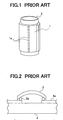
- FIG.1 is a perspective view showing a configuration of a deformed semiconductor chip that is described in Japanese Laid-Open Patent Publication No. 2001-118982.
- the semiconductor chip 1 shown in this drawing is wrapped around a cylinder-shaped support substrate 2 to be deformed into a cylinder shape.
- electrode pads 1a of the semiconductor chip 1 are arranged in a longitudinal direction with respect to the cylinder shape and these electrode pads 1a may be used to interconnect to another similar cylindrically deformed semiconductor chip.
- FIG.2 is a side view showing a configuration of a deformed semiconductor chip that is described in Japanese Laid-Open Patent Publication No. 11-345823.
- One side of the semiconductor chip 3 shown in this drawing has solder bumps 3a mounted thereon as external connection electrodes, and the semiconductor chip 3 is deformed in a manner such this side forms a concave surface.
- the solder bumps 3a are connected to a wiring portion 4a of an interposer 4. According to this configuration, even when the interposer 4 is thermally deformed, stress created between the semiconductor chip 3 and the interposer 4 (i.e, at the solder bumps 3a) may be alleviated since the semiconductor chip may easily deform (bend).
- the semiconductor chip 1 is wrapped around a cylindrical substrate 2, and thereby, the weight of the semiconductor device may increase. Also, depending on the connection state of the chips (e.g., when the chips wrapped around a cylinder structure are mounted on top of each other), the chips that are to be mounted may need to be interconnected, and thereby the pads of the chips may have to be adjusted. Consequently, redesigning of the chip structure may be required, and the conventional semiconductor chip may not be used in its present form. Also, the semiconductor chip 1 has to be precisely wrapped around the cylinder substrate 2, and in turn measures for realizing such effect need to be contemplated.
- the chip when a semiconductor chip is deformed and flip chip mounted as in the case of semiconductor chip 3 of FIG.2, the chip is thin and lacks strength so that a crack may be generated upon connecting the chip to the interposer or sealing the structure with resin, for example. Further, since the semiconductor chip is deformed into an arc shape, the positioning accuracy of the connection portion between the interposer and the semiconductor chip may be low.
- a more specific object of the present invention is to provide a semiconductor device that uses one or more thin semiconductor chips and to deform the semiconductor chips so that the semiconductor chips may be arranged in a spatially-efficient manner.
- a semiconductor device in one aspect of the present invention, includes at least one semiconductor chip, a setting member that is formed on a surface of the semiconductor chip and is configured to set the semiconductor chip into a deformed shape corresponding to a substantially cylinder shape or a curved shape, a package substrate to which the deformed semiconductor chip is flip chip connected, a sealing resin that seals the semiconductor chip onto the package substrate, and an external connection terminal that is provided on the package substrate.
- the deformed shape of a semiconductor chip may be maintained by the setting member, and the semiconductor chip may be flip chip connected to the package substrate in its present state.
- the setting member may also function as a strengthening member for preventing cracking of the semiconductor chip.
- the setting member corresponds to a resin layer that is formed on an inner side surface of the substantially cylinder shaped or curve shaped semiconductor chip.
- the thickness of the semiconductor chip is preferably no more than 50 ⁇ m.
- a semiconductor device may include plural semiconductor chips that are flip chip connected to each other.
- the plural semiconductor chips may include a first substantially cylinder shaped semiconductor chip, and a second substantially cylinder shaped semiconductor chip having a diameter that is greater than that of the first semiconductor chip, the second semiconductor chip being arranged around the outer periphery of the first semiconductor chip.
- an end portion of the first semiconductor chip may protrude and extend from an end portion of the second semiconductor chip and the first semiconductor chip and the package substrate may be flip chip connected.
- the plural semiconductor chips may include a first curve shaped semiconductor chip, and a second curve shaped semiconductor chip having a greater curve dimension than that of the first semiconductor chip, the second semiconductor chip being arranged around the outer periphery of the first semiconductor chip.
- an end portion of the second semiconductor chip may be arranged to extend beyond an end portion of the first semiconductor chip, and the second semiconductor chip and the package substrate may be flip chip connected.
- a semiconductor device may include plural curve shaped semiconductor chips in different sizes.
- a smaller-sized semiconductor chip may be arranged to be accommodated within a space created by the curved shape of a larger-sized semiconductor chip.
- the plural semiconductor chips may be individually flip chip connected to the package substrate.
- a smaller-sized semiconductor chip may be flip chip connected to a larger-sized semiconductor chip, and the larger semiconductor chip may be flip chip connected to the package substrate.
- a semiconductor device may include plural flat semiconductor chips that are layered, and a deformed semiconductor chip that is flip chip connected to the package substrate and an uppermost semiconductor chip layer of the flat semiconductor chip layers having a circuit formation surface that is facing upward.
- the present invention according to another aspect provides a method for manufacturing a semiconductor device having a deformed semiconductor chip, the method including the steps of supporting a flat semiconductor chip, applying a liquid resin on a surface of the flat semiconductor chip, deforming the flat semiconductor chip in a manner such that the resin-applied surface of the semiconductor chip forms an inner side of the deformed semiconductor chip, hardening the liquid resin and setting the semiconductor chip into a substantially cylinder shape or a curved shape, and flip chip mounting the semiconductor chip to a package substrate.
- the step of applying liquid resin may be conducted after deforming the semiconductor chip.
- FIG.3 is a cross-sectional diagram showing a semiconductor device according to a first embodiment of the present invention.
- the semiconductor device shown in FIG.3 includes a semiconductor chip 10 that is bent into a substantially cylinder structure.
- the semiconductor chip 10 is bent in a manner such that bumps 10a as external connection terminals face outward.
- the bumps 10a may be made of solder or gold, for example.
- the bumps 10a which are provided at the outer edges of the semiconductor chip 10, are aligned into two rows that extend in the longitudinal direction with respect to the cylinder structure.
- coating material 11 such as resin is applied as a setting member. In this way, the cylinder structure of the semiconductor chip 10 may be retained by the resin layer.
- the semiconductor chip 10 is connected to a package substrate (interposer) 12 via the bumps 10a. More specifically, bumps 10a of the semiconductor chip 10 are flip chip connected to the interposer 12. The semiconductor chip 10 is sealed onto the interposer 12 by a sealing resin 13. At the outer side of the interposer 12, solder balls 14 are provided as external connection terminals of the semiconductor device.
- the thickness of the semiconductor chip 10 is arranged to be relatively thin, preferably less than or equal to 50 ⁇ m.
- the size of the interposer 12 to be implemented may be smaller compared to a case in which the semiconductor chip 10 has a flat configuration. In this way, the horizontal projected area of the semiconductor device may be reduced.
- FIG.4 is a block diagram illustrating an internal circuit of a semiconductor chip that is used in a memory device according a prior art example.
- a data input circuit 15 and a data output circuit 16 may be connected to one electrode pad 17.
- a write circuit 19 and a read circuit 20 may be provided at respective sides of a memory cell array 18.
- the data output circuit 16 is arranged close to the read circuit 20, the distance between the data input circuit and the write circuit 19 is increased, thereby increasing the length of a wiring 21 within the semiconductor chip for connecting these two circuits.
- a long wiring within the chip hinders high speed reading operations of the device.
- short wiring formed on the interposer may be used in place of the above-described wiring within the semiconductor chip of the prior art. Details of this feature are described below.
- FIG.5 is a block diagram illustrating an internal circuit of the cylindrical semiconductor chip 10 that is used as a memory device according to an embodiment of the present invention.
- FIG.6 is a diagram illustrating an internal configuration of the semiconductor chip 10 in a case where the circuit of FIG.5 is implemented.
- the data input circuit 15 is arranged close to the write circuit 19
- the data output circuit 16 is arranged close to the read circuit 20.
- Data input terminals 22 are arranged close to the data output circuit 16 and the read circuit 20 in an aligned state.
- Data output terminals 23 are arranged close to the data input circuit 15 and the write circuit 19 in an aligned state.
- the row of the data input terminals 22 corresponds to electrodes aligned at one side of the semiconductor chip 10
- the row of the data output terminals 23 corresponds to electrodes aligned at the other side of the semiconductor chip 10.
- a clock (CLK) terminal 24 is included in each of the row of data input terminals 22 and the row of data output terminals 23.
- the row of data input terminals 22 and the row of output terminals 23 close in on each other to form two parallel lines.
- the electrodes of the semiconductor chip 10 formed into such a configuration are connected to electrode pads 25 of the interposer 12 as is illustrated in FIG.7, and thereby, data input terminals 22 and their corresponding data output terminals 23 may be interconnected by wiring 26 formed on the interposer 12.
- short wiring may be used in place of the long wiring 21 (FIG.4) formed in the semiconductor chip of the prior art so that a high speed operation may be realized.
- FIG.8 is a perspective view of a deformation jig for shaping a semiconductor chip into a cylinder shape that is used in a first method of forming a semiconductor chip.
- the deformation jig 30 shown in FIG.8 includes a center support part 31 and arc-shaped movable parts 32 that are arranged at the sides of the support part 31 in a rotatable manner.
- the support part 31 includes vacuum suction holes 31a that are configured to realize vacuum adhesion of the center portion of the semiconductor chip 10 when the semiconductor chip 10 is flat. Also, electro-thermal lines 32a are provided in the movable parts 32 in order to generate heat upon realizing deformation of the semiconductor chip with the deformation jig 30.
- FIGS.9A ⁇ 9C illustrate the process of forming a semiconductor chip into a cylinder structure according to the first method.
- the surface of a flat semiconductor chip 10 on which the bumps 10a are mounted is adhered by vacuum suction to the support part 31.
- a coating material 11 is applied to the other side of the semiconductor chip 10.
- the movable parts 32 are rotated so that the semiconductor chip may gradually be deformed into the arc configuration of the movable parts 32.
- the movable parts 32 are rotated toward each other until the semiconductor chip 10 is formed into a substantially cylindrical configuration as is shown in FIG.9C.
- the coating material 11 applied to the inner side of the semiconductor chip 10 is heat-cured by the electro-thermal lines 32a of the movable parts 32.
- the movable parts 32 are moved back to their original positions, the vacuum adhesion is released, and the semiconductor chip 10 that is formed into a substantially cylindrical configuration is removed from the deformation jig 30.
- the cylindrical configuration of the semiconductor chip 10 may be maintained by the cured coating material 11.
- the coating material 11 may alternatively be applied to the inner side of the semiconductor chip 10 and cured after the semiconductor chip 10 is deformed into a cylindrical configuration.
- the rotation of the moving parts 32 may be stopped before the semiconductor chip 10 is formed into a cylindrical configuration, and the coating material 11 may be applied to the inner side of the semiconductor chip 10 in an arched state, after which the coating material is hardened to form a semiconductor chip 10 with a curved configuration.
- the coating material 11 is not limited to a particular material, quick dry liquid material such as epoxy resin may preferably be used. Also, since the semiconductor chip 10 is sealed by sealing resin 13, the coating material 11 is preferably made of resin that has a characteristic similar to that of the sealing resin 13 so that separation of the semiconductor package structure due to stress generated upon re-flow when mounting the semiconductor device may be prevented.
- the coating material 11 is preferably arranged to be thin in order to avoid disfiguration of the semiconductor chip 10 due to contraction of the coating material 11, for example.
- the coating material 11 is preferably arranged to be thinner than the semiconductor chip 10, and may be arranged to be as thin as possible.
- the temperature for heat-curing the coating material 11 is preferably arranged to be no more than 200 °C upon considering the effects on the semiconductor chip 10.
- the coating material 11 may be applied in a wafer state, and after deforming the semiconductor chip using the deformation jig 30, the coating material may be heated and set to a desired shape.
- the semiconductor chip is not wrapped around a cylinder substrate as in the prior art example; rather, the semiconductor chip is deformed into a cylinder shape without using a cylinder shaped member so that the weight of the semiconductor chip structure may be decreased.
- the mounting structure of the semiconductor chip is not changed from that of the conventional semiconductor chip in which electrode pads of the semiconductor chip are wrapped around a cylinder shaped member, and thereby, a semiconductor chip with the conventional design may be used in the semiconductor device of the present invention.
- the semiconductor chip 10 By setting the shape of the semiconductor chip using the coating material 11, the semiconductor chip 10 may be formed and set to an arbitrary shape, and the strength of the semiconductor chip 10 may be increased. Thereby, chip cracks may be prevented during a flip chip connection operation and/or a resin sealing operation, for example.
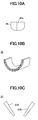
- FIGS.10A, 10B, and 10C are diagrams illustrating deformation jigs that are used in shaping a semiconductor chip into a cylinder structure according to the second method.
- FIGS.11A ⁇ 11E are diagrams illustrating the process of shaping the semiconductor chip into a cylinder structure according to the second method.
- the inner side of a semiconductor chip i.e., the side of the semiconductor chip 10 opposite the side on which the bumps 10a are provided
- a support jig 35 of FIG.10A the semiconductor chip 10 is vacuum-adhered at holes 35a provided at the support jig 35.
- the semiconductor chip 10 that is supported by the support jig 35 is placed on a curved jig 36, and pressed into the curved jig 36 by the support jig 35.
- the curved jig 36 corresponds to a jig provided with elasticity that has a cross-sectional configuration close to a semi-circle.
- the semiconductor chip 10 As the semiconductor chip 10 is pressed by the support jig 35, the semiconductor chip 10 is gradually deformed into a shape defined by the inner side of the curved jig 36 as is shown in FIG.11C.
- the shape of the semiconductor chip 10 defined by the inner side of the curved jig 36 may be maintained by providing vacuum adhesion means to the curved jig 36.
- an electro-thermal line may be provided in the curved jig 36 for heating the curved jig 36.
- the support jig 35 is removed from the semiconductor chip 10, and the curved jig 36 is pushed at both sides by a push jig 37 (including parts 37A and 37B).
- a push jig 37 including parts 37A and 37B.
- the cross-sectional configuration of the curved jig 36 is deformed into a shape closer to a circle than a semi-circle.
- the semiconductor chip 10 arranged within the curved jig 36 may be deformed into a substantially cylindrical shape.
- a coating material 11 may be applied to the semiconductor chip 10 when it is in a state as illustrated in FIG.11D or FIG.11E, and the coating material may be hardened thereafter so as to set the semiconductor chip 10 in a cylindrical shape.
- FIG.12 is a cross-sectional diagram illustrating one example of a semiconductor device that implements plural cylinder shaped semiconductor chips according to an embodiment of the present invention.
- three semiconductor chips 10 are flip chip connected to a package substrate (interposer) 38, and sealed thereto by a sealing resin 39.
- solder balls 40 are provided as external connection terminals.
- the horizontal projected area of the semiconductor device may be reduced compared to a case of using the same number of flat semiconductor chips.
- each of the plural semiconductor chips may be flip chip connected to the interposer 38.
- FIG.13 is a cross-sectional diagram showing another example of a semiconductor device that implements plural cylinder shaped semiconductor chips according to an embodiment of the present invention.
- three semiconductor chips 10 are provided on each side of an interposer 41, that is, a total of six semiconductor chips are flip chip connected to the respective sides of the interposer 41 and sealed thereto by a sealing resin 42.
- Solder balls 43 as external connection terminals are provided at the outer sides of the sealing resin 43 provided on one side of the interposer 41, and the solder balls 43 are arranged to have a dimension that is greater than the thickness of the sealing resin 42.
- semiconductor chips 10 shown in the example of FIG.13 are slightly oval shaped, and in this way, the thickness of the sealing resin may be reduced.
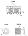
- FIG.14 is a cross-sectional diagram showing another example of a semiconductor device that implements plural cylinder shaped semiconductor chips.
- the semiconductor chips are arranged into a double layered cylinder structure.
- FIG.15 is a cross-sectional view of the semiconductor chips shown in FIG.14.
- a cylindrical semiconductor chip 10A is provided as an inner perimeter chip
- a cylindrical semiconductor chip 10B is provided on the periphery of the semiconductor chip 10A as an outer perimeter chip. In this way, plural semiconductor chips may be formed into an integrated structure.
- the semiconductor chips 10A and 10B may be flip chip connected to the interposer 45 as a single semiconductor chip structure, and the semiconductor chips 10A and 10B may be sealed onto the interposer 45 by sealing resin 46.
- solder balls 47 are provided on the other side of the interposer 45.
- FIG.16 is a side view of an end portion of the double-layered cylindrical semiconductor chip structure.
- the surface of the outer semiconductor chip 10B on which bumps are to be formed (circuit formation surface) faces the inner semiconductor chip 10A and corresponds to an inner perimeter surface of the cylinder structure. Thereby, external connection terminals cannot be formed on the outer semiconductor chip 10B.
- the surface of the inner semiconductor chip 10A on which bumps are to be formed (circuit formation surface) corresponds to an outer perimeter surface of the cylinder structure that faces outward.
- the end portions of the inner semiconductor chip are arranged to protrude from the end portions of the outer semiconductor chip 10B, and bumps 10Aa as external connection terminals are provided at the outer surface of the end portions of the inner semiconductor chip 10A.
- the outer semiconductor chip 10B is connected to the interposer 45 via wiring within the inner semiconductor chip 10A and the bumps 10Aa.
- plural semiconductor chips may be arranged within the semiconductor device in a spatially efficient manner, and the packaging density of the semiconductor chips may be increased.
- FIG.17 is a cross-sectional diagram illustrating a configuration of a semiconductor device according to the second embodiment of the present invention.
- the semiconductor device shown in FIG.17 includes a curved semiconductor chip 50.
- the semiconductor chip 50 is formed into a curved structure in a manner such that the surface of the semiconductor chip 50 that has bumps 50a formed thereon as external connection terminals (circuit formation surface) forms the inner side of the curved structure.
- the bumps 50a may be made of solder or gold, for example.
- a coating material 11 such as resin is applied to the circuit formation surface of the semiconductor chip 50, after which the coating material 11 is cured to form a resin layer.
- the semiconductor chip 50 is connected to a package substrate (interposer) 52 via the bumps 50a.
- the bumps 50a of the semiconductor chip 50 provide flip chip connection to the interposer 52.
- the semiconductor chip 50 is sealed onto the interposer by a sealing resin 53.
- solder balls 54 are provided as external connection terminals of the semiconductor device.
- the thickness of the semiconductor chip 50 is preferably arranged to be no more than 50 ⁇ m.
- the size of the interposer may be reduced compared to the case of using a flat semiconductor chip. Thereby, the horizontal projected area of the semiconductor device may be reduced.
- the methods used to form the cylinder shaped semiconductor chip 10 according to the first embodiment may be used to form the curved semiconductor chip 50.
- the deformation jig 30 shown in FIG.8 may be used to form the curved semiconductor chip 50.
- the semiconductor chip 50 in a flat state may be fixed to the support part 31, in a manner such that the chip surface to be held in contact with the support part 31 is reversed with respect to the case of forming the cylindrical semiconductor chip 10.
- the bumps 50a are arranged to face downward upon being fixed to the support part 31.
- the rotation of the movable parts 32 is stopped in the state shown in FIG.9B, and coating material 11 applied to the semiconductor chip is cured to set the semiconductor chip 50 into a curved shape.
- the semiconductor chip 50 may also be formed by the deformation jigs 35 and 36 shown in FIGS.10A and 10B.
- the semiconductor chip 50 in a flat state may be fixed to the support part 31, in a manner such that the chip surface to be held in contact with the support part 31 is reversed with respect to the case of forming the cylindrical semiconductor chip 10, and the bumps 50a are arranged to face downward upon being fixed to the support part 35.
- the coating material 11 is applied to the semiconductor chip 50 in the state shown in FIG.11C, after which the coating material 11 is cured to form the semiconductor chip 50 that is set to a curved shape.
- FIG.18 is a cross-sectional perspective view of a deformation jig for forming a curved semiconductor chip.
- the deformation jig 55 shown in FIG.18 corresponds to a block-shaped jig that has a concave portion 55a that forms a space at the center portion of its bottom section.
- This jig 55 includes vacuum suction holes 55b that open through the center of this space formed at the bottom section.
- an injection path 55c for injecting a coating material 56 opens through this space at the bottom section.
- an electro-thermal line 50d for heating the jig is embedded close to the bottom section.
- the back surface (opposite the circuit formation surface) of a flat-shaped semiconductor chip 50 is placed at the bottom section of the deformation jig 55 as is shown in FIG.19A.
- the space created by the concave portion 55a of the jig 55 is arranged to be positioned at the center portion of the semiconductor chip 50.
- the coating material 56 is applied to the circuit formation surface of the semiconductor chip 50.
- the semiconductor chip 50 is vacuum-adhered via the vacuum suction holes 55b so that the semiconductor chip 50 may be deformed into a curved structure as is shown in FIG.19B.
- the coating material 56 is injected from the injection path 55c to be placed between the semiconductor chip 50 and the bottom surface of the concave portion of the deformation jig 55, after which the coating material 56 is heated by the electro-thermal line 50d and cured.
- the semiconductor chip 50 may be set to a curved shape by the coating material 56 placed on the circuit formation surface side of the semiconductor chip 50 and on the opposite side thereof.
- FIG.20 is a cross-sectional view of another deformation jig for forming a curved semiconductor chip.
- the deformation jig 60 shown in FIG.20 includes a center support portion 60A for supporting the center portion of the semiconductor chip 50, and edge support portions 60B and 60C for supporting the respective edges of the semiconductor chip 50.
- the center support portion 60A and the edge support portions 60B and 60C are arranged to adhere a flat shaped semiconductor chip 50 via vacuum suction holes 60a.
- FIG.20 shows a state in which the flat shaped semiconductor chip 50 is adhered to the deformation jig 60.
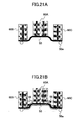
- the center support portion 60A is arranged to move with respect to the edge support portions 60B and 60C so that the semiconductor chip 50 is deformed into a curved shape as is shown in FIG.21A from the state shown in FIG.20.
- the semiconductor chip 50 may be formed into a curved shape by deforming the portions in between the center portion and the edge portions of the semiconductor chip 50 while retaining the flat configurations of the center portion and the edge portions that are supported by the center support portion 60A and the edge support portions 60B and 60C.
- the coating material 56 is applied to the circuit formation surface side and the other side of the semiconductor chip 50 and cured thereafter (see FIG.21B).
- the semiconductor chip 50 may be set to a curved shape.
- the semiconductor chips 50 are preferably arranged in a manner such that the extending direction of the space openings formed by the curved structures of the semiconductor chips 50 are in alignment with the flowing direction of the sealing resin, which is indicated by arrows in the present drawing. Specifically, the positions of gates 65 for injecting the sealing resin are adjusted so that the sealing resin may easily flow and fill into the spaces created by the semiconductor chips 50 and the interposer 52. Such an arrangement may also be applied to a case in which the cylindrical semiconductor chips 10 of the first embodiment are used.
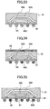
- FIG.23 is a cross-sectional view of a semiconductor device having a configuration in which a smaller-sized semiconductor chip is accommodated within a space created by the curved shape of a larger-sized semiconductor chip.
- a large semiconductor chip 50A is formed into a curved structure
- a smaller-sized semiconductor chip 50B that is also formed into a curved structure is placed inside the curvature of the semiconductor chip 50A.
- an even smaller-sized semiconductor chip 50C that is flat-shaped in placed within the curvature of the semiconductor chip 50B.
- each of the semiconductor chips 50A, 50B, and 50C is flip chip connected to the interposer 52 and is sealed thereto by a sealing resin 53.
- each of the semiconductor chips may be flip chip connected to the interposer 52.
- a heat sink 66 may be provided on the upper surface of the sealing resin 53 as is shown in FIG.24.
- the semiconductor chips may be mounted starting with the smallest semiconductor chip, and the semiconductor chips may be collectively deformed thereafter to realize the flip chip connection of the semiconductor chips at once. In this way, the manufacturing process steps may be reduced.
- the semiconductor chips since such method may cause a degradation in the connection accuracy between the interposer and the semiconductor chips, and may also result in an increase in the thickness of the semiconductor chips to thereby hinder the deformation of the semiconductor chips, it is preferred that the semiconductor chips be deformed and flip chip connected individually.
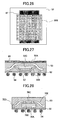
- FIG.25 is a cross-sectional view of another exemplary semiconductor device having a configuration in which a smaller-sized semiconductor chip is accommodated within a space created by the curved shape of a larger-sized semiconductor chip.
- the semiconductor chip 50B is positioned upside down so as to be flip chip connected to the semiconductor chip 50A.
- the semiconductor chip 50C is arranged inside a space created between the semiconductor chip 50A and the semiconductor chip 50B.
- the semiconductor chip 50C is flip chip connected to the semiconductor chip 50B.
- the back side (opposite the circuit formation surface) of the semiconductor chip 50B is arranged to face the interposer 52, thereby, a solid wiring layer 67 such as a copper layer may be formed on the interposer 52 as is shown in FIG.26 so that heat transfer from the semiconductor chip 50B may be increased.
- a heat sink 66 made of a metal plate may be provided on the upper surface of the sealing resin 53 as is shown in FIG.27 to further increase heat transfer.
- Other alternative measures may also be taken to increase heat transfer, including the introduction of thermal balls, and/or the use of a sealing resin with good heat transfer characteristics to reduce heat transfer resistance.
- the semiconductor chips are flip chip connected to each other. In this way the length of the connection wiring between the chips may be shortened and high speed operation may be realized.
- FIG.28 is a cross-sectional view of another exemplary semiconductor device that implements plural semiconductor chips.
- plural flat semiconductor chips are connected to the interposer 52, and the uppermost semiconductor chip is connected to the interposer by being deformed.
- semiconductor chips 70A and 70B are layered in a manner such that their respective back surfaces face each other, and the semiconductor chip 70A is flip chip connected to the interposer 52.
- the semiconductor chip 70B is arranged so that its circuit formation surface faces upward.
- the semiconductor chip 70B is further flip chip connected with a semiconductor chip 70C. It is noted that in a conventional MCP (multi-chip package), a semiconductor chip and an interposer are generally connected via a bonding wire; however, in the present example shown in FIG.28, deformed semiconductor chips 70D and 70E are used instead of a bonding wire.
- MCP multi-chip package
- the semiconductor chips 70D and 70E that are used for connecting the multilayered semiconductor chip structure to the interposer 52 may be suitably deformed into a desired shape so that the thickness of the multilayered semiconductor chip structure may not be restricted. Also, even in a case where a large number of electrode pads are provided, and/or a large number of semiconductor chips are mounted, connection of the semiconductor chips may be integrally realized by using the deformed chip to establish flip chip connection between the uppermost semiconductor chip and the interposer so that the electrode pads of each of the semiconductor chips do not have to be individually connected. Accordingly, connection between the semiconductor chips and the interposer may be realized in a short period of time.
- the type of semiconductor chip used as the uppermost semiconductor chip 70C and the semiconductor chips 70D and 70E for realizing connection with the lower semiconductor chips is not limited to a particular type of semiconductor chip, and for example, a semiconductor chip including a semiconductor circuit may be used, or a semiconductor chip that merely includes wiring patterns may be used as well.
- FIG.29 is a plan view showing an exemplary wiring arrangement of the semiconductor chip 70D.
- electrode pads 71 to be connected to electrode pads of the semiconductor chip 70B are arranged into a row on one side edge of the semiconductor chip 70D
- electrode pads 72 to be connected to electrode pads of the interposer 52 are arranged into a row on the other side edge of the semiconductor chip 70D.
- pattern wiring 73 connects the electrode pad 71 to an electrode pad 72 to thereby connect the semiconductor chip 70B to the interposer 52.
- Pattern wiring 74 connects a circuit within the semiconductor chip 70D to the interposer 52.
- Pattern wiring 75 connects a circuit within the semiconductor chip 70D to the semiconductor chip 70B.
- Pattern wiring 76 interconnects the semiconductor chip 70B, the semiconductor chip 70D, and the interposer 52 simultaneously.
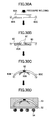
- FIGS.30A ⁇ 30D are diagrams illustrating the process of forming a semiconductor device by collectively deforming plural semiconductor chips at once.
- plural semiconductor chips 80A, 80B, and 80C are flip chip connected to each other as is shown in FIG.30A, and an underfill material 81 is placed in between the semiconductor chips to set the semiconductor chips as is shown in FIG.30B.
- the set semiconductor chip structure of semiconductor chips 80A, 80B, and 80C is integrally deformed (bent) using one of the above-described deformation methods, for example, after which resin 82 as a setting member is placed in the space created between the semiconductor chips 80A, 80B, and 80C to be cured thereat as is shown in FIG.30C.
- the deformed semiconductor chip structure of semiconductor chips 80A, 80B, and 80C is flip chip connected to the interposer 52 and sealed thereon by a sealing resin 53 as is shown in FIG.30D.
- plural semiconductor chips may be integrally deformed. Also, deformation of a small semiconductor chip (e.g., semiconductor chip 80A) that cannot be easily deformed on its own may be realized using the present method.
- a small semiconductor chip e.g., semiconductor chip 80A
- the present invention is not limited to such arrangement, and for example, the semiconductor chips 80B and 80C may be arranged into one single semiconductor chip.
Landscapes
- Wire Bonding (AREA)
Abstract
Description
Claims (14)
- A semiconductor device, characterized by comprising:at least one semiconductor chip;a setting member that is formed on a surface of the semiconductor chip and is configured to set the semiconductor chip into a deformed shape corresponding to one of a substantially cylinder shape and a curved shape;a package substrate to which the deformed semiconductor chip is flip chip connected;a sealing resin that seals the semiconductor chip onto the package substrate; andan external connection terminal that is provided on the package substrate.
- The semiconductor device as claimed in claim 1, wherein the setting member corresponds to a resin layer that is formed on an inner side surface of the substantially cylinder shaped or curve shaped semiconductor chip.
- The semiconductor device as claimed in claim 1, wherein a thickness of the semiconductor chip is no more than 50 µm.
- The semiconductor device as claimed in claim 1, further comprising:a plurality of the semiconductor chips which semiconductor chips are flip chip connected to each other.
- The semiconductor device as claimed in claim 4, wherein:the semiconductor chips include a first substantially cylinder shaped semiconductor chip, and a second substantially cylinder shaped semiconductor chip having a diameter that is greater than a diameter of the first semiconductor chip, the second semiconductor chip being arranged around the periphery of the first semiconductor chip.
- The semiconductor device as claimed in claim 5, wherein:an end portion of the first semiconductor chip protrudes and extends from an end portion of the second semiconductor chip, and the first semiconductor chip and the package substrate are flip chip connected.
- The semiconductor device as claimed in claim 4, wherein:the semiconductor chips include a first curve shaped semiconductor chip, and a second curve shaped semiconductor chip having a greater curve dimension than a curve dimension of the first semiconductor chip, the second semiconductor chip being arranged around the periphery of the first semiconductor chip.
- The semiconductor device as claimed in claim 7, wherein:an end portion of the second semiconductor chip extends beyond an end portion of the first semiconductor chip, and the second semiconductor chip and the package substrate are flip chip connected.
- The semiconductor device as claimed in claim 1, further comprising:wherein a smaller-sized semiconductor chip of the semiconductor chips is arranged to be accommodated within a space created by the curved shape of a larger-sized semiconductor chip of the semiconductor chips.a plurality of curve shaped semiconductor chips that have different sizes;
- The semiconductor device as claimed in claim 9, wherein:the semiconductor chips are individually flip chip connected to the package substrate.
- The semiconductor device as claimed in claim 9, wherein:a smaller-sized semiconductor chip of the semiconductor chips is flip chip connected to a larger-sized semiconductor chip of the semiconductor chips, and a largest semiconductor chip of the semiconductor chips is flip chip connected to the package substrate.
- The semiconductor device as claimed in claim 1, further comprising:a plurality of flat semiconductor chips which semiconductor chips are layered; anda deformed semiconductor chip that is flip chip connected to the package substrate and to an uppermost semiconductor chip of the flat semiconductor chips which uppermost semiconductor chip is arranged to have a circuit formation surface facing upward.
- A method for manufacturing a semiconductor device having a deformed semiconductor chip, the method characterized by comprising the steps of:supporting a flat semiconductor chip;applying a liquid resin on a surface of the flat semiconductor chip;deforming the flat semiconductor chip in a manner such that the resin-applied surface of the semiconductor chip forms an inner side of the deformed semiconductor chip;curing the liquid resin and setting the semiconductor chip into one of a substantially cylinder shape and a curved shape; andflip chip mounting the semiconductor chip onto a package substrate.
- The semiconductor device manufacturing method as claimed in claim 13, wherein the step of applying liquid resin is conducted after deforming the semiconductor chip.
Applications Claiming Priority (1)
| Application Number | Priority Date | Filing Date | Title |
|---|---|---|---|
| PCT/JP2002/008193 WO2004015758A1 (en) | 2002-08-09 | 2002-08-09 | Semiconductor device and method for manufacturing the same |
Publications (3)
| Publication Number | Publication Date |
|---|---|
| EP1528593A1 true EP1528593A1 (en) | 2005-05-04 |
| EP1528593A4 EP1528593A4 (en) | 2008-02-27 |
| EP1528593B1 EP1528593B1 (en) | 2009-07-22 |
Family
ID=31513601
Family Applications (1)
| Application Number | Title | Priority Date | Filing Date |
|---|---|---|---|
| EP02758823A Expired - Lifetime EP1528593B1 (en) | 2002-08-09 | 2002-08-09 | Semiconductor device and method for manufacturing the same |
Country Status (8)
| Country | Link |
|---|---|
| US (1) | US7138723B2 (en) |
| EP (1) | EP1528593B1 (en) |
| JP (1) | JP4299783B2 (en) |
| KR (1) | KR100630588B1 (en) |
| CN (1) | CN100401486C (en) |
| DE (1) | DE60233077D1 (en) |
| TW (1) | TWI234827B (en) |
| WO (1) | WO2004015758A1 (en) |
Cited By (1)
| Publication number | Priority date | Publication date | Assignee | Title |
|---|---|---|---|---|
| EP3084824A4 (en) * | 2013-12-19 | 2017-08-16 | Intel Corporation | Flexibly-wrapped integrated circuit die |
Families Citing this family (15)
| Publication number | Priority date | Publication date | Assignee | Title |
|---|---|---|---|---|
| CN101310570B (en) * | 2005-11-18 | 2010-11-10 | 日本电气株式会社 | Mounting substrate and electronic device |
| KR100780691B1 (en) * | 2006-03-29 | 2007-11-30 | 주식회사 하이닉스반도체 | Folding Chip Planar Stack Package |
| US9114004B2 (en) | 2010-10-27 | 2015-08-25 | Iridium Medical Technology Co, Ltd. | Flexible artificial retina devices |
| US8954156B2 (en) | 2010-10-27 | 2015-02-10 | National Tsing Hua University | Methods and apparatuses for configuring artificial retina devices |
| US8530265B2 (en) | 2010-10-27 | 2013-09-10 | National Tsing Hua University | Method of fabricating flexible artificial retina devices |
| US8613135B2 (en) | 2011-05-06 | 2013-12-24 | National Tsing Hua University | Method for non-planar chip assembly |
| US9155881B2 (en) | 2011-05-06 | 2015-10-13 | Iridium Medical Technology Co, Ltd. | Non-planar chip assembly |
| KR101772255B1 (en) * | 2011-05-06 | 2017-08-28 | 이리듐 메디칼 테크놀로지 컴퍼니 리미티드 | A non-planar integrated circuit device |
| TWI507182B (en) * | 2011-10-26 | 2015-11-11 | Iridium Medical Technology Co Ltd | Methods of fabricating flexible artificial retina devices |
| TWI473220B (en) * | 2012-01-10 | 2015-02-11 | 精材科技股份有限公司 | Semiconductor stack structure and its preparation method |
| US10446728B2 (en) * | 2014-10-31 | 2019-10-15 | eLux, Inc. | Pick-and remove system and method for emissive display repair |
| CN107112317B (en) * | 2014-12-24 | 2019-07-05 | 日本精工株式会社 | Power semiconductor modular and the electric power steering apparatus for using it |
| KR20170060372A (en) * | 2015-11-24 | 2017-06-01 | 에스케이하이닉스 주식회사 | Flexible package using warped chip |
| US12020972B2 (en) | 2020-04-29 | 2024-06-25 | Semiconductor Components Industries, Llc | Curved semiconductor die systems and related methods |
| DE102020122662B4 (en) * | 2020-08-31 | 2025-11-06 | Infineon Technologies Ag | AD:JR:cs bending semiconductor chip for interconnection at different vertical planes and method for manufacturing a package |
Family Cites Families (17)
| Publication number | Priority date | Publication date | Assignee | Title |
|---|---|---|---|---|
| JPH01244625A (en) * | 1988-03-26 | 1989-09-29 | Mitsubishi Electric Corp | Semiconductor device |
| JP3227589B2 (en) * | 1992-12-24 | 2001-11-12 | 株式会社日立製作所 | Semiconductor device |
| US6255599B1 (en) * | 1997-08-18 | 2001-07-03 | Ibm | Relocating the neutral plane in a PBGA substrate to eliminate chip crack and interfacial delamination |
| US6448665B1 (en) * | 1997-10-15 | 2002-09-10 | Kabushiki Kaisha Toshiba | Semiconductor package and manufacturing method thereof |
| JPH11186326A (en) * | 1997-12-24 | 1999-07-09 | Shinko Electric Ind Co Ltd | Semiconductor device |
| JPH11345823A (en) * | 1998-05-29 | 1999-12-14 | Sony Corp | Semiconductor chip flip-chip mounting method and mounting jig |
| JP3168987B2 (en) * | 1998-07-09 | 2001-05-21 | 日本電気株式会社 | Mounting structure of surface mount type semiconductor device |
| WO2000021121A1 (en) * | 1998-10-05 | 2000-04-13 | Seiko Epson Corporation | Semiconductor device and method for producing the same |
| TW460927B (en) * | 1999-01-18 | 2001-10-21 | Toshiba Corp | Semiconductor device, mounting method for semiconductor device and manufacturing method for semiconductor device |
| JP4321926B2 (en) * | 1999-10-19 | 2009-08-26 | 富士通株式会社 | Semiconductor device, semiconductor integrated device and manufacturing method thereof |
| JP3414342B2 (en) * | 1999-11-25 | 2003-06-09 | 日本電気株式会社 | Mounting structure and mounting method of integrated circuit chip |
| JP3265301B2 (en) | 2000-06-05 | 2002-03-11 | 株式会社東芝 | Semiconductor device and manufacturing method thereof |
| JP4126891B2 (en) * | 2001-08-03 | 2008-07-30 | セイコーエプソン株式会社 | Manufacturing method of semiconductor device |
| JP2003051568A (en) * | 2001-08-08 | 2003-02-21 | Nec Corp | Semiconductor device |
| US20040104463A1 (en) * | 2002-09-27 | 2004-06-03 | Gorrell Robin E. | Crack resistant interconnect module |
| US6949404B1 (en) * | 2002-11-25 | 2005-09-27 | Altera Corporation | Flip chip package with warpage control |
| US6888238B1 (en) * | 2003-07-09 | 2005-05-03 | Altera Corporation | Low warpage flip chip package solution-channel heat spreader |
-
2002
- 2002-08-09 CN CNB028292510A patent/CN100401486C/en not_active Expired - Fee Related
- 2002-08-09 KR KR1020047021035A patent/KR100630588B1/en not_active Expired - Fee Related
- 2002-08-09 EP EP02758823A patent/EP1528593B1/en not_active Expired - Lifetime
- 2002-08-09 DE DE60233077T patent/DE60233077D1/en not_active Expired - Lifetime
- 2002-08-09 JP JP2004527308A patent/JP4299783B2/en not_active Expired - Fee Related
- 2002-08-09 WO PCT/JP2002/008193 patent/WO2004015758A1/en not_active Ceased
- 2002-08-15 TW TW091118453A patent/TWI234827B/en not_active IP Right Cessation
-
2004
- 2004-12-08 US US11/006,664 patent/US7138723B2/en not_active Expired - Fee Related
Cited By (1)
| Publication number | Priority date | Publication date | Assignee | Title |
|---|---|---|---|---|
| EP3084824A4 (en) * | 2013-12-19 | 2017-08-16 | Intel Corporation | Flexibly-wrapped integrated circuit die |
Also Published As
| Publication number | Publication date |
|---|---|
| TWI234827B (en) | 2005-06-21 |
| JPWO2004015758A1 (en) | 2005-12-02 |
| KR20050009759A (en) | 2005-01-25 |
| KR100630588B1 (en) | 2006-10-04 |
| US20050082684A1 (en) | 2005-04-21 |
| US7138723B2 (en) | 2006-11-21 |
| DE60233077D1 (en) | 2009-09-03 |
| CN1633704A (en) | 2005-06-29 |
| JP4299783B2 (en) | 2009-07-22 |
| EP1528593B1 (en) | 2009-07-22 |
| WO2004015758A1 (en) | 2004-02-19 |
| CN100401486C (en) | 2008-07-09 |
| EP1528593A4 (en) | 2008-02-27 |
Similar Documents
| Publication | Publication Date | Title |
|---|---|---|
| EP1528593B1 (en) | Semiconductor device and method for manufacturing the same | |
| TWI447880B (en) | Stacked semiconductor package, method of forming the same, and electronic system including the same | |
| US6610560B2 (en) | Chip-on-chip based multi-chip module with molded underfill and method of fabricating the same | |
| JP4441328B2 (en) | Semiconductor device and manufacturing method thereof | |
| US6822324B2 (en) | Wafer-level package with a cavity and fabricating method thereof | |
| CN101378051B (en) | Semiconductor device and manufacturing method thereof | |
| CN116169110A (en) | A chip and packaging method | |
| US20020063319A1 (en) | Direct-downset flip-chip package assembly and method of fabricating the same | |
| JP2001144218A (en) | Semiconductor device and method of manufacturing semiconductor device | |
| JP2009506572A (en) | Microfeature assemblies including interconnect structures and methods for forming such interconnect structures | |
| JP2001223297A (en) | Semiconductor device, method of manufacturing semiconductor device, and method of stacking semiconductor device | |
| JPH07245360A (en) | Semiconductor package and manufacturing method thereof | |
| WO1999034436A1 (en) | Semiconductor device | |
| TW201411792A (en) | Semiconductor device manufacturing method | |
| JP2008258522A (en) | Manufacturing method of semiconductor device | |
| CN118197993A (en) | Chip fan-out packaging method and chip fan-out packaging structure | |
| JP2004165283A (en) | Semiconductor device | |
| US20080116586A1 (en) | Methods for manufacturing thermally enhanced flip-chip ball grid arrays | |
| US20080009096A1 (en) | Package-on-package and method of fabricating the same | |
| JP4565931B2 (en) | Manufacturing method of semiconductor device | |
| KR20180036947A (en) | Interconnect structure for semiconductor package and method of fabricating the interconnect structure | |
| CN115274615A (en) | Small chip interconnection packaging structure based on silicon bridge and manufacturing method thereof | |
| US20090166879A1 (en) | Semiconductor package | |
| JP2000307032A (en) | Chip scale package and manufacturing method thereof | |
| JP4452767B2 (en) | Semiconductor device and manufacturing method thereof |
Legal Events
| Date | Code | Title | Description |
|---|---|---|---|
| PUAI | Public reference made under article 153(3) epc to a published international application that has entered the european phase |
Free format text: ORIGINAL CODE: 0009012 |
|
| 17P | Request for examination filed |
Effective date: 20050105 |
|
| AK | Designated contracting states |
Kind code of ref document: A1 Designated state(s): AT BE BG CH CY CZ DE DK EE ES FI FR GB GR IE IT LI LU MC NL PT SE SK TR |
|
| RBV | Designated contracting states (corrected) |
Designated state(s): DE FR GB |
|
| A4 | Supplementary search report drawn up and despatched |
Effective date: 20080124 |
|
| RAP1 | Party data changed (applicant data changed or rights of an application transferred) |
Owner name: FUJITSU MICROELECTRONICS LIMITED |
|
| GRAP | Despatch of communication of intention to grant a patent |
Free format text: ORIGINAL CODE: EPIDOSNIGR1 |
|
| RIN1 | Information on inventor provided before grant (corrected) |
Inventor name: SUZUKI, TAKAAKI Inventor name: HIRAOKA, TETSUYA Inventor name: OZAWA, KANAME Inventor name: TAKASHIMA, AKIRA Inventor name: MATSUZAKI, YASUROU Inventor name: AIBA, KAZUYUKI |
|
| GRAS | Grant fee paid |
Free format text: ORIGINAL CODE: EPIDOSNIGR3 |
|
| GRAA | (expected) grant |
Free format text: ORIGINAL CODE: 0009210 |
|
| AK | Designated contracting states |
Kind code of ref document: B1 Designated state(s): DE FR GB |
|
| REG | Reference to a national code |
Ref country code: GB Ref legal event code: FG4D |
|
| REF | Corresponds to: |
Ref document number: 60233077 Country of ref document: DE Date of ref document: 20090903 Kind code of ref document: P |
|
| PGFP | Annual fee paid to national office [announced via postgrant information from national office to epo] |
Ref country code: FR Payment date: 20090728 Year of fee payment: 8 |
|
| PGFP | Annual fee paid to national office [announced via postgrant information from national office to epo] |
Ref country code: GB Payment date: 20091028 Year of fee payment: 8 |
|
| PLBE | No opposition filed within time limit |
Free format text: ORIGINAL CODE: 0009261 |
|
| STAA | Information on the status of an ep patent application or granted ep patent |
Free format text: STATUS: NO OPPOSITION FILED WITHIN TIME LIMIT |
|
| 26N | No opposition filed |
Effective date: 20100423 |
|
| GBPC | Gb: european patent ceased through non-payment of renewal fee |
Effective date: 20100809 |
|
| REG | Reference to a national code |
Ref country code: FR Ref legal event code: ST Effective date: 20110502 |
|
| PG25 | Lapsed in a contracting state [announced via postgrant information from national office to epo] |
Ref country code: FR Free format text: LAPSE BECAUSE OF NON-PAYMENT OF DUE FEES Effective date: 20100831 |
|
| PG25 | Lapsed in a contracting state [announced via postgrant information from national office to epo] |
Ref country code: GB Free format text: LAPSE BECAUSE OF NON-PAYMENT OF DUE FEES Effective date: 20100809 |
|
| REG | Reference to a national code |
Ref country code: DE Ref legal event code: R082 Ref document number: 60233077 Country of ref document: DE Representative=s name: REICHERT & LINDNER PARTNERSCHAFT PATENTANWAELT, DE |
|
| REG | Reference to a national code |
Ref country code: DE Ref legal event code: R082 Ref document number: 60233077 Country of ref document: DE Representative=s name: REICHERT & LINDNER PARTNERSCHAFT PATENTANWAELT, DE Effective date: 20150512 Ref country code: DE Ref legal event code: R081 Ref document number: 60233077 Country of ref document: DE Owner name: SOCIONEXT INC., YOKOHAMA-SHI, JP Free format text: FORMER OWNER: FUJITSU SEMICONDUCTOR LTD., YOKOHAMA, KANAGAWA, JP Effective date: 20150512 |
|
| PGFP | Annual fee paid to national office [announced via postgrant information from national office to epo] |
Ref country code: DE Payment date: 20170801 Year of fee payment: 16 |
|
| REG | Reference to a national code |
Ref country code: DE Ref legal event code: R119 Ref document number: 60233077 Country of ref document: DE |
|
| PG25 | Lapsed in a contracting state [announced via postgrant information from national office to epo] |
Ref country code: DE Free format text: LAPSE BECAUSE OF NON-PAYMENT OF DUE FEES Effective date: 20190301 |