EP1526516A2 - Optical recording medium, substrate for optical recording medium and optical disk device - Google Patents
Optical recording medium, substrate for optical recording medium and optical disk device Download PDFInfo
- Publication number
- EP1526516A2 EP1526516A2 EP05002015A EP05002015A EP1526516A2 EP 1526516 A2 EP1526516 A2 EP 1526516A2 EP 05002015 A EP05002015 A EP 05002015A EP 05002015 A EP05002015 A EP 05002015A EP 1526516 A2 EP1526516 A2 EP 1526516A2
- Authority
- EP
- European Patent Office
- Prior art keywords
- recording medium
- address
- optical
- disk device
- tracks
- Prior art date
- Legal status (The legal status is an assumption and is not a legal conclusion. Google has not performed a legal analysis and makes no representation as to the accuracy of the status listed.)
- Granted
Links
Images


Classifications
-
- G—PHYSICS
- G11—INFORMATION STORAGE
- G11B—INFORMATION STORAGE BASED ON RELATIVE MOVEMENT BETWEEN RECORD CARRIER AND TRANSDUCER
- G11B7/00—Recording or reproducing by optical means, e.g. recording using a thermal beam of optical radiation by modifying optical properties or the physical structure, reproducing using an optical beam at lower power by sensing optical properties; Record carriers therefor
- G11B7/007—Arrangement of the information on the record carrier, e.g. form of tracks, actual track shape, e.g. wobbled, or cross-section, e.g. v-shaped; Sequential information structures, e.g. sectoring or header formats within a track
-
- G—PHYSICS
- G11—INFORMATION STORAGE
- G11B—INFORMATION STORAGE BASED ON RELATIVE MOVEMENT BETWEEN RECORD CARRIER AND TRANSDUCER
- G11B20/00—Signal processing not specific to the method of recording or reproducing; Circuits therefor
- G11B20/10—Digital recording or reproducing
-
- G—PHYSICS
- G11—INFORMATION STORAGE
- G11B—INFORMATION STORAGE BASED ON RELATIVE MOVEMENT BETWEEN RECORD CARRIER AND TRANSDUCER
- G11B7/00—Recording or reproducing by optical means, e.g. recording using a thermal beam of optical radiation by modifying optical properties or the physical structure, reproducing using an optical beam at lower power by sensing optical properties; Record carriers therefor
- G11B7/004—Recording, reproducing or erasing methods; Read, write or erase circuits therefor
- G11B7/005—Reproducing
- G11B7/0053—Reproducing non-user data, e.g. wobbled address, prepits, BCA
-
- G—PHYSICS
- G11—INFORMATION STORAGE
- G11B—INFORMATION STORAGE BASED ON RELATIVE MOVEMENT BETWEEN RECORD CARRIER AND TRANSDUCER
- G11B7/00—Recording or reproducing by optical means, e.g. recording using a thermal beam of optical radiation by modifying optical properties or the physical structure, reproducing using an optical beam at lower power by sensing optical properties; Record carriers therefor
- G11B7/007—Arrangement of the information on the record carrier, e.g. form of tracks, actual track shape, e.g. wobbled, or cross-section, e.g. v-shaped; Sequential information structures, e.g. sectoring or header formats within a track
- G11B7/00718—Groove and land recording, i.e. user data recorded both in the grooves and on the lands
-
- G—PHYSICS
- G11—INFORMATION STORAGE
- G11B—INFORMATION STORAGE BASED ON RELATIVE MOVEMENT BETWEEN RECORD CARRIER AND TRANSDUCER
- G11B7/00—Recording or reproducing by optical means, e.g. recording using a thermal beam of optical radiation by modifying optical properties or the physical structure, reproducing using an optical beam at lower power by sensing optical properties; Record carriers therefor
- G11B7/007—Arrangement of the information on the record carrier, e.g. form of tracks, actual track shape, e.g. wobbled, or cross-section, e.g. v-shaped; Sequential information structures, e.g. sectoring or header formats within a track
- G11B7/00745—Sectoring or header formats within a track
-
- G—PHYSICS
- G11—INFORMATION STORAGE
- G11B—INFORMATION STORAGE BASED ON RELATIVE MOVEMENT BETWEEN RECORD CARRIER AND TRANSDUCER
- G11B7/00—Recording or reproducing by optical means, e.g. recording using a thermal beam of optical radiation by modifying optical properties or the physical structure, reproducing using an optical beam at lower power by sensing optical properties; Record carriers therefor
- G11B7/24—Record carriers characterised by shape, structure or physical properties, or by the selection of the material
- G11B7/2407—Tracks or pits; Shape, structure or physical properties thereof
- G11B7/24085—Pits
Definitions
- the present invention relates to an optical recording medium for recording and/or reproducing information by irradiation with a laser beam or the like, a substrate for the optical recording medium, and an optical disk device.
- the recording medium includes a transparent substrate of a general disk shape and a recording layer provided on the substrate.
- the recording layer is formed of a thin film in which a phase change is caused between an amorphous state and a crystalline state.
- Phase change materials known to be used for the recording layer include an alloy film mainly containing elements such as Ge, Sb, Te, and In of, for example, a GeSbTe alloy.
- information is recorded in such a manner that the recording layer is partially brought into an amorphous state to form a mark and erased in such a manner that the mark in the amorphous state is brought into a crystalline state.
- the recording layer is brought into the amorphous state.
- the recording layer is brought into the crystalline state.
- guide grooves in the form of a spiral or concentric circles for tracking a laser beam in recording and reproducing information and addresses for indicating a position on the recording medium, each composed of uneven strings of pits, are provided to form an initial state of the substrate.
- a region between the adjoining grooves is referred to as a land.
- information is recorded on one of the groove and the land, and the other serves as a guard band for separating adjoining recording tracks from each other.
- DVD-RAM digital versatile disc-read only memory
- the groove and the land are set so as to be substantially equal in width.
- Recording media of this kind have employed a method in which address information is recorded in an intermediate position between a pair of adjoining groove and land tracks so that with respect to the pair of adjoining groove and land tracks, one address information is recorded.
- an address recorded in this manner in the intermediate position between the pair of adjoining groove and land tracks is referred to as "an intermediate address”.
- an intermediate address method a method in which the intermediate address is used to record address information so that the address information is shared by a pair of adjoining tracks.
- JP10(1998)-31822 A a method of demodulating address information in a recording medium employing the intermediate address method is disclosed.
- a sum signal or a difference signal of electric signals output from a photodetector provided in an optical head of an optical disk device is used to demodulate the address information.
- the photodetector includes light receiving parts divided into two parts in a direction parallel to tracks on the recording medium.
- a signal quality assessment was conducted using reproduction signals obtained by reproducing an address on a recording medium formed in the following manner.
- address pits 9 were arranged in the form of staggered pit strings so that with respect to a distance (a track pitch) Tp between a center line of a groove track 7 and a center line of a land track 8, center lines of strings of the address pits 9 were shifted in a radial direction of the recording medium (namely, a direction perpendicular to the tracks) at a distance of about Tp/2 from the center lines of the groove tracks 7 and the center lines of the land tracks 8.
- a pit width W of the address pits 9 was the same as the track pitch Tp (namely, the same as the width of the groove track 7 and the width of the land track 8).
- the reproduction signals obtained by reproducing the address differed in symmetry between the sum signal and the difference signal.
- an optimum condition under which excellent signal quality could be obtained was found by adjusting the lengths of the address pits.
- no condition was found under which such signal quality could be obtained for both of the sum signal and the difference signal at the same time.
- a recording medium suited for address information demodulation using the sum signal is employed in an optical disk device in which address information demodulation is performed using the difference signal.
- a recording medium suited for address information demodulation using the difference signal is employed in an optical disk device in which address information demodulation is performed using the sum signal.
- the present invention is intended to solve the conventional problem as described above. It is an object of the present invention to provide an optical recording medium that allows reliable address information reproduction using either a sum signal or a difference signal of electric signals output from a photodetector provided in an optical head of an optical disk device, thereby enhancing compatibility of the optical disk device being used and a substrate for the optical recording medium. It is another object of the present invention to provide an optical disk device that allows an increased reproduction margin in demodulating address information, thereby achieving high-accuracy address detection.
- address information can be reproduced with reliability using either a sum signal or a difference signal of electric signals output from light receiving parts, divided into two parts in a direction parallel to tracks, of a photodetector provided in the optical head of the optical disk device, thereby enhancing compatibility of the optical disk device being used.
- an optical disk device of the present invention includes a first address demodulating circuit for demodulating address information using the sum signal and a second address demodulating circuit for demodulating address information using the difference signal, and thus an address can be detected with high accuracy based on information obtained from the first and second address demodulating circuits.
- a first embodiment relates to an optical recording medium and a substrate used in manufacturing the optical recording medium.
- the inventors of the present invention conducted a test using recording media having the structure employing the intermediate address method described with reference to FIG. 10 that were manufactured by varying the pit width W of the address pits 9.
- the recording media were reproduced for the measurement of the quality of a sum signal and a difference signal of electric signals that were output from a photodetector provided in an optical head of an optical disk device in an address area on the respective recording media.
- the test has shown that an address reproduction signal having excellent signal quality can be obtained in both of the cases of the sum signal and the difference signal by setting the pit width W of the address pits so as to fall within a fixed range. This will be explained in the following.
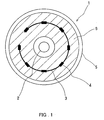
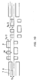
- FIG. 1 is a plan view schematically showing the configuration of the optical recording medium of the present invention
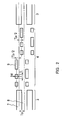
- FIG. 2 is a fragmentary enlarged plan view showing the structure of an address area on the optical recording medium of the present invention.
- an optical recording medium 1 includes a substrate 5 made of polycarbonate that has a thickness of 0.6 mm, a recording layer 6 provided on the substrate 5, of a multi-layered thin film formed by laminating a ZnS-SiO 2 thin film as a dielectric, a GeSbTe alloy thin film as a phase change material, a ZnS-SiO 2 thin film, and an Al alloy thin film in this order, and a protective layer (not shown) provided on the recording layer 6, formed of an ultraviolet hardening resin.
- the GeSbTe alloy thin film is brought into a crystalline state by irradiation with a laser beam to form an initial state of the film.
- the recording layer 6 has a reflectance of about 20% with respect to a light beam having a wavelength of 650 nm.
- the substrate 5 includes a center hole 2 for fitting the optical recording medium to an optical disk device, tracks 3 in the form of a spiral, and addresses 4 for indicating a position on the optical recording medium.
- the tracks 3 and the addresses 4 are shown exemplarily in the form of exaggerated portions of the tracks 3 and the addresses 4, respectively.
- the tracks 3 are composed of groove tracks 7 having a depth of about 65 nm and a width of about 0.62 ⁇ m and land tracks 8 having a width of about 0.62 ⁇ m that are provided alternately. Information is recorded on both of the groove tracks 7 and the land tracks 8.
- the address 4 is encoded by a (8-16) modulation method and composed of uneven strings of pits (address pits) 9 and spaces.
- the address pits 9 have a length L varied between 3T and 11T by 0.5T with respect to a reference clock T.
- the address pits 9 having a depth of about 65 nm are arranged in the form of staggered pit strings so that center lines of strings of the address pits 9 are shifted in a radial direction of the recording medium (namely, a direction perpendicular to the tracks 3) at a distance of about 0.31 ⁇ m, which is one-half a track pitch Tp (namely, the width of the groove tracks 7 and the width of the land tracks 8) from center lines of the groove tracks 7 and center lines of the land tracks 8.
- Tp namely, the width of the groove tracks 7 and the width of the land tracks
- FIGs. 3 and 5 are block diagrams exemplarily showing optical disk devices used in the test.
- FIG. 3 shows the optical disk device in which address information is demodulated using a sum signal 15S of electric signals output from a photodetector.
- the recording medium 1 shown in FIG. 1 is mounted to the optical disk device.
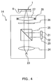
- FIG. 4 shows the structure of an optical head 14 of the optical disk device.
- a light beam emitted from a semiconductor laser as a light source 23 is focused on the recording medium 1 through a collimator lens 24, a beam splitter 25, a 1/4 wave plate 26, and an objective lens 27.
- Afocal point of the light beam is controlled so as to be on the recording layer 6 in the recording medium 1 by adjusting the position of the objective lens 27 using a voice coil 28.
- the light beam reflected from the recording layer 6 goes back to the beam splitter 25 through the objective lens 27 and the 1/4 wave plate 26.
- the light beam is reflected from the beam splitter 25 and is incident on a photodetector 20 to be converted to an electric signal.
- the photodetector 20 includes light receiving parts 21 and 22 divided into two parts in a direction parallel to the tracks on the recording medium 1.
- the semiconductor laser 23 has a laser wavelength of 650 nm and the objective lens 27 has a numerical aperture of 0.60.
- the optical disk device shown in FIG. 3 includes a spindle motor 10 for rotating the recording medium 1 mounted thereto, a controller 11 for receiving and transmitting data 11S to be recorded or reproduced or the like, a modulator 12 for converting data to be recorded to a recording signal, a laser driving circuit 13 for driving the semiconductor laser according to the recording signal, and the optical head 14 having the semiconductor laser for focusing a laser beam on the recording medium 1 to record information and obtaining a reproduction signal using the reflected laser beam.
- the optical disk device further includes a summing amplifier 15 for outputting the sum signal 15S of electric signals output from the light receiving parts 21 and 22 of the photodetector 20 provided in the optical head 14, a differential amplifier 16 for outputting a difference signal 16S of electric signals output from the light receiving parts 21 and 22, an address demodulating circuit 17 for demodulating address information using the sum signal 15S, a data demodulating circuit 18 for demodulating data recorded on the tracks using the sum signal 15S, and a tracking controlling circuit 19 for controlling the optical head 14 so that a laser beam scans a track on the recording medium 1 properly based on the difference signal 16S.
- a summing amplifier 15 for outputting the sum signal 15S of electric signals output from the light receiving parts 21 and 22 of the photodetector 20 provided in the optical head 14
- a differential amplifier 16 for outputting a difference signal 16S of electric signals output from the light receiving parts 21 and 22, an address demodulating circuit 17 for demodulating address information using the sum signal 15S, a data demodulating circuit
- FIG. 5 shows the optical disk device in which address information is demodulated using a difference signal 16S of electric signals output from a photodetector 20.
- the optical disk device has substantially the same configuration as that of the optical disk device described with reference to FIG. 3 and is different only in the method of demodulating address information.
- address information is demodulated using the difference signal 16S output from a differential amplifier 16.
- the optical disk device is of the same configuration as that of the optical disk device shown in FIG. 3, and thus the duplicate descriptions are omitted by referring to FIG. 5 in which like reference characters denote the corresponding components shown in FIG. 3.
- optical disk devices and the recording medium described above with reference to FIGs. 3 and 5, in which the recording medium is irradiated with a laser beam having an intensity of 1 mW while being rotated at a linear velocity of 8.2 m/second were used to measure signal quality of a signal output from the summing amplifier 15 in an address area on the recording medium (namely, a sum signal of electric signals output from the photodetector 20 provided in the optical head 14) and a signal output from the differential amplifier 16 in the address area on the optical recording medium (namely, a difference signal of electric signals output from the photodetector 20 provided in the optical head 14).
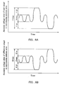
- FIGs. 6(A) and 6(B) are waveform charts exemplarily showing absolute voltage values of the sum signal and the difference signal output in reproducing the address area.
- the signal quality was measured by calculating an asymmetry X1 and an asymmetry X2 defined as follows.
- FIG. 7 shows asymmetry of the sum signal and asymmetry of the difference signal with respect to each address pit width. From these results, it is shown that the asymmetry of the difference signal (denoted by open circles in FIG. 7) has lower values than those of the asymmetry of the sum signal (denoted by solid circles in FIG. 7). It is also shown that the smaller an address pit width is, the smaller the difference in asymmetry values between these signals.
- FIGs. 8(A) and 8(B) show the relationship between an address pit and a beam spot of a laser beam in address reproduction.
- a beam spot 30 is on an address pit 9a having a length of 11T.
- the beam spot 30 is on an address pit 9b having a length of 3T.
- a transverse direction indicates a peripheral direction of a recording medium, and the beam spot 30 scans in a direction indicated by an arrow.
- the address pit does not have edge portions in the peripheral direction that lie within the beam spot 30, so that the reflected laser beam is diffracted only in a direction perpendicular to the peripheral direction (namely, a radial direction of the recording medium) as in the case where the laser beam is reflected from a track area.
- the address pit has the edge portions in the peripheral direction that lie within the beam spot 30, so that the reflected laser beam is diffracted in the peripheral direction as well as the direction perpendicular to the peripheral direction.
- a portion of the reflected laser beam that is diffracted in the peripheral direction is incident on both of the light receiving parts 21 and 22 described with reference to FIG. 4. This produces the effect of decreasing the output of the differential amplifier 16.
- the asymmetry of the difference signal has lower values than those of the asymmetry of the sum signal.
- a large difference in asymmetry values between the sum signal and the difference signal leads to the difficulty in obtaining excellent signal quality for both of the sum signal and the difference signal.
- the difference in asymmetry values between the sum signal and the difference signal is required to be not more than 0.1 to secure the range.
- the recording media having a pit width of not more than 0.39 ⁇ m have proven to satisfy this condition. In a recording medium having a pit width of less than 0.23 ⁇ m, a sufficient signal intensity of a reproduction signal cannot be obtained. Therefore, preferably, a pit width falls within the range of 0.23 ⁇ m to 0.39 ⁇ m.
- an asymmetry value may vary depending on variations in address pit length
- the asymmetry of the difference signal always has a lower value than that of the asymmetry of the sum signal. Therefore, by forming an address pit into a shape that allows an asymmetry value of the sum signal to fall within the range of 0 to 0.05, an address reproduction signal having further improved signal quality can be obtained in both of the cases of the sum signal and the difference signal.
- the recording layer may be formed of a material other than a GeSbTe alloy such as a magneto-optical recording material and an organic dye.
- the recording medium that can be used is not limited to an erasable recording medium that allows rewriting of information.
- a recordable recording medium on which information can be recorded only once also may be used.
- the substrate may be formed of a material other than polycarbonate such as glass and acrylic.
- the address pits may be arranged in a row instead of in the form of staggered pit strings.
- the tracks 3 were in the form of a spiral. However, the tracks 3 may take the form of concentric circles.
- a second embodiment relates to an optical disk device employing the optical recording medium described above.
- FIG. 9 is a block diagram showing the configuration of an optical disk device of an embodiment according to the present invention.
- the optical disk device has substantially the same configuration as those described with reference to FIGs. 3 and 5 and is different only in the method of demodulating address information.
- a first address demodulating circuit 17 demodulates address information using a sum signal 15S output from a summing amplifier 15, and a second address demodulating circuit 29 demodulates address information using a difference signal 16S output from a differential amplifier 16.
- These two address demodulating circuits 17 and 29 are provided in the device, so that even when the recording medium 1 has variations in address forming conditions, an address can be detected with high accuracy using at least one of the address demodulating circuits. Furthermore, in the case where the optical recording medium of the present invention described in the first embodiment is used as the recording medium 1, address information can be demodulated in both of the address demodulating circuits 17 and 29, and thus the accuracy of address detection further can be increased.
Abstract
Description
- The present invention relates to an optical recording medium for recording and/or reproducing information by irradiation with a laser beam or the like, a substrate for the optical recording medium, and an optical disk device.
- Among optical recording media that have come into focus as large-capacity and high-density memories is an erasable optical recording medium that allows rewriting of information. Currently, the development of the erasable optical recording medium has been underway. In one form of the erasable optical recording medium, information is recorded and erased utilizing thermal energy generated by irradiation with a laser beam. The recording medium includes a transparent substrate of a general disk shape and a recording layer provided on the substrate. The recording layer is formed of a thin film in which a phase change is caused between an amorphous state and a crystalline state.
- Phase change materials known to be used for the recording layer include an alloy film mainly containing elements such as Ge, Sb, Te, and In of, for example, a GeSbTe alloy. In many cases, information is recorded in such a manner that the recording layer is partially brought into an amorphous state to form a mark and erased in such a manner that the mark in the amorphous state is brought into a crystalline state. When heated to a temperature equal to or higher than the melting point and subsequently cooled at a speed higher than a fixed speed, the recording layer is brought into the amorphous state. When heated to a temperature equal to or higher than the crystallization temperature and equal to or lower than the melting point, the recording layer is brought into the crystalline state.
- Generally, on the substrate, guide grooves (grooves) in the form of a spiral or concentric circles for tracking a laser beam in recording and reproducing information and addresses for indicating a position on the recording medium, each composed of uneven strings of pits, are provided to form an initial state of the substrate. A region between the adjoining grooves is referred to as a land. In many cases, information is recorded on one of the groove and the land, and the other serves as a guard band for separating adjoining recording tracks from each other.
- In recent years, the improvement in processing capabilities of various kinds of information-processing equipment has allowed the processing of an increasing amount of information. Thus, a recording medium has been requested to allow larger-capacity information recording and reproducing. In order to attain this, DVD-RAM or the like has employed a method in which information is recorded on both of the groove and the land, so that a higher track density can be obtained. In this case, the groove and the land are set so as to be substantially equal in width. Recording media of this kind have employed a method in which address information is recorded in an intermediate position between a pair of adjoining groove and land tracks so that with respect to the pair of adjoining groove and land tracks, one address information is recorded.
- An address recorded in this manner in the intermediate position between the pair of adjoining groove and land tracks is referred to as "an intermediate address". Further, a method in which the intermediate address is used to record address information so that the address information is shared by a pair of adjoining tracks is referred to as "an intermediate address method".
- In JP10(1998)-31822 A, a method of demodulating address information in a recording medium employing the intermediate address method is disclosed. In the method, a sum signal or a difference signal of electric signals output from a photodetector provided in an optical head of an optical disk device is used to demodulate the address information. The photodetector includes light receiving parts divided into two parts in a direction parallel to tracks on the recording medium.
- In this connection, a signal quality assessment was conducted using reproduction signals obtained by reproducing an address on a recording medium formed in the following manner. As shown in FIG. 10,
address pits 9 were arranged in the form of staggered pit strings so that with respect to a distance (a track pitch) Tp between a center line of agroove track 7 and a center line of aland track 8, center lines of strings of theaddress pits 9 were shifted in a radial direction of the recording medium (namely, a direction perpendicular to the tracks) at a distance of about Tp/2 from the center lines of thegroove tracks 7 and the center lines of theland tracks 8. In the recording medium, a pit width W of theaddress pits 9 was the same as the track pitch Tp (namely, the same as the width of thegroove track 7 and the width of the land track 8). As a result, the reproduction signals obtained by reproducing the address differed in symmetry between the sum signal and the difference signal. For each of the sum signal and the difference signal, an optimum condition under which excellent signal quality could be obtained was found by adjusting the lengths of the address pits. However, no condition was found under which such signal quality could be obtained for both of the sum signal and the difference signal at the same time. - That is, neither of the following cases allows sufficient signal quality to be obtained, which has led to a problem of a limited margin for reproduction conditions. In one case, a recording medium suited for address information demodulation using the sum signal is employed in an optical disk device in which address information demodulation is performed using the difference signal. In the other case, a recording medium suited for address information demodulation using the difference signal is employed in an optical disk device in which address information demodulation is performed using the sum signal. In other words, in each of the optical disk devices in which address information demodulation is performed using the sum signal and the difference signal, respectively, a permissible level of variations in address forming conditions of recording media is limited.
- The present invention is intended to solve the conventional problem as described above. It is an object of the present invention to provide an optical recording medium that allows reliable address information reproduction using either a sum signal or a difference signal of electric signals output from a photodetector provided in an optical head of an optical disk device, thereby enhancing compatibility of the optical disk device being used and a substrate for the optical recording medium. It is another object of the present invention to provide an optical disk device that allows an increased reproduction margin in demodulating address information, thereby achieving high-accuracy address detection.
- In order to achieve the aforementioned objects, an optical recording medium (or a substrate for the optical recording medium) of the present invention is an optical recording medium (or a substrate for the optical recording medium) employing the intermediate address method, in which an address pit width (namely, a length of an address pit in an intermediate position of a depth (or a height) of a concave or a convex of the address pit in a radial direction of the recording medium) W satisfies the relationship:
with respect to a laser wavelength λ and a numerical aperture NA of an objective lens of an optical head of an optical disk device being used, and a track pitch Tp of the recording medium. According to this configuration, address information can be reproduced with reliability using either a sum signal or a difference signal of electric signals output from light receiving parts, divided into two parts in a direction parallel to tracks, of a photodetector provided in the optical head of the optical disk device, thereby enhancing compatibility of the optical disk device being used. - Furthermore, an optical disk device of the present invention includes a first address demodulating circuit for demodulating address information using the sum signal and a second address demodulating circuit for demodulating address information using the difference signal, and thus an address can be detected with high accuracy based on information obtained from the first and second address demodulating circuits.
-
- FIG. 1 is a plan view schematically showing the configuration of an optical recording medium of an embodiment according to the present invention.
- FIG. 2 is a fragmentary enlarged plan view of the optical recording medium of the embodiment according to the present invention.
- FIG. 3 is a block diagram showing a first configuration of a conventional optical disk device for an optical recording medium.
- FIG. 4 is a structural view showing an optical head of the conventional optical disk device for the optical recording medium.
- FIG. 5 is a block diagram showing a second configuration of the conventional optical disk device for the optical recording medium.
- FIG. 6 shows waveforms of address reproduction signals.
- FIG. 7 is a graph showing the relationship between a pit width of an address and asymmetry of reproduction signals obtained by reproducing the address.
- FIG. 8 shows the relationship between an address pit and a beam spot.
- FIG. 9 is a block diagram showing the configuration of an optical disk device for the optical recording medium according to the present invention.
- FIG. 10 is a fragmentary expanded plan view of the conventional optical recording medium.
-
- Hereinafter, the optical recording medium and the optical disk device of the present invention will be described with reference to the appended drawings.
- A first embodiment relates to an optical recording medium and a substrate used in manufacturing the optical recording medium.
- The inventors of the present invention conducted a test using recording media having the structure employing the intermediate address method described with reference to FIG. 10 that were manufactured by varying the pit width W of the
address pits 9. In the test, the recording media were reproduced for the measurement of the quality of a sum signal and a difference signal of electric signals that were output from a photodetector provided in an optical head of an optical disk device in an address area on the respective recording media. The test has shown that an address reproduction signal having excellent signal quality can be obtained in both of the cases of the sum signal and the difference signal by setting the pit width W of the address pits so as to fall within a fixed range. This will be explained in the following. - FIG. 1 is a plan view schematically showing the configuration of the optical recording medium of the present invention, and FIG. 2 is a fragmentary enlarged plan view showing the structure of an address area on the optical recording medium of the present invention. In FIG. 1, an optical recording medium 1 includes a
substrate 5 made of polycarbonate that has a thickness of 0.6 mm, arecording layer 6 provided on thesubstrate 5, of a multi-layered thin film formed by laminating a ZnS-SiO2 thin film as a dielectric, a GeSbTe alloy thin film as a phase change material, a ZnS-SiO2 thin film, and an Al alloy thin film in this order, and a protective layer (not shown) provided on therecording layer 6, formed of an ultraviolet hardening resin. The GeSbTe alloy thin film is brought into a crystalline state by irradiation with a laser beam to form an initial state of the film. Therecording layer 6 has a reflectance of about 20% with respect to a light beam having a wavelength of 650 nm. Thesubstrate 5 includes acenter hole 2 for fitting the optical recording medium to an optical disk device, tracks 3 in the form of a spiral, and addresses 4 for indicating a position on the optical recording medium. In FIG. 1, thetracks 3 and theaddresses 4 are shown exemplarily in the form of exaggerated portions of thetracks 3 and theaddresses 4, respectively. - In FIG. 2, the
tracks 3 are composed ofgroove tracks 7 having a depth of about 65 nm and a width of about 0.62 µm andland tracks 8 having a width of about 0.62 µm that are provided alternately. Information is recorded on both of the groove tracks 7 and the land tracks 8. Theaddress 4 is encoded by a (8-16) modulation method and composed of uneven strings of pits (address pits) 9 and spaces. The address pits 9 have a length L varied between 3T and 11T by 0.5T with respect to a reference clock T. The address pits 9 having a depth of about 65 nm are arranged in the form of staggered pit strings so that center lines of strings of the address pits 9 are shifted in a radial direction of the recording medium (namely, a direction perpendicular to the tracks 3) at a distance of about 0.31 µm, which is one-half a track pitch Tp (namely, the width of the groove tracks 7 and the width of the land tracks 8) from center lines of the groove tracks 7 and center lines of the land tracks 8. In the test conducted this time, substrates were prepared by varying the width W of the address pits 9 between 0.23 µm and 0.40 µm and used. These substrates were molded by an injection molding method using a stamper made of Ni. - FIGs. 3 and 5 are block diagrams exemplarily showing optical disk devices used in the test. FIG. 3 shows the optical disk device in which address information is demodulated using a
sum signal 15S of electric signals output from a photodetector. In FIG. 3, the recording medium 1 shown in FIG. 1 is mounted to the optical disk device. FIG. 4 shows the structure of anoptical head 14 of the optical disk device. - In FIG. 4, a light beam emitted from a semiconductor laser as a
light source 23 is focused on the recording medium 1 through acollimator lens 24, abeam splitter 25, a 1/4wave plate 26, and anobjective lens 27. Afocal point of the light beam is controlled so as to be on therecording layer 6 in the recording medium 1 by adjusting the position of theobjective lens 27 using avoice coil 28. The light beam reflected from therecording layer 6 goes back to thebeam splitter 25 through theobjective lens 27 and the 1/4wave plate 26. Then, the light beam is reflected from thebeam splitter 25 and is incident on aphotodetector 20 to be converted to an electric signal. Thephotodetector 20 includeslight receiving parts semiconductor laser 23 has a laser wavelength of 650 nm and theobjective lens 27 has a numerical aperture of 0.60. - The optical disk device shown in FIG. 3 includes a
spindle motor 10 for rotating the recording medium 1 mounted thereto, acontroller 11 for receiving and transmittingdata 11S to be recorded or reproduced or the like, amodulator 12 for converting data to be recorded to a recording signal, alaser driving circuit 13 for driving the semiconductor laser according to the recording signal, and theoptical head 14 having the semiconductor laser for focusing a laser beam on the recording medium 1 to record information and obtaining a reproduction signal using the reflected laser beam. The optical disk device further includes a summingamplifier 15 for outputting thesum signal 15S of electric signals output from thelight receiving parts photodetector 20 provided in theoptical head 14, adifferential amplifier 16 for outputting adifference signal 16S of electric signals output from thelight receiving parts address demodulating circuit 17 for demodulating address information using thesum signal 15S, adata demodulating circuit 18 for demodulating data recorded on the tracks using thesum signal 15S, and atracking controlling circuit 19 for controlling theoptical head 14 so that a laser beam scans a track on the recording medium 1 properly based on thedifference signal 16S. - FIG. 5 shows the optical disk device in which address information is demodulated using a
difference signal 16S of electric signals output from aphotodetector 20. The optical disk device has substantially the same configuration as that of the optical disk device described with reference to FIG. 3 and is different only in the method of demodulating address information. As shown in FIG. 5, in anaddress demodulating circuit 29, address information is demodulated using thedifference signal 16S output from adifferential amplifier 16. Other than this point, the optical disk device is of the same configuration as that of the optical disk device shown in FIG. 3, and thus the duplicate descriptions are omitted by referring to FIG. 5 in which like reference characters denote the corresponding components shown in FIG. 3. - The optical disk devices and the recording medium described above with reference to FIGs. 3 and 5, in which the recording medium is irradiated with a laser beam having an intensity of 1 mW while being rotated at a linear velocity of 8.2 m/second, were used to measure signal quality of a signal output from the summing
amplifier 15 in an address area on the recording medium (namely, a sum signal of electric signals output from thephotodetector 20 provided in the optical head 14) and a signal output from thedifferential amplifier 16 in the address area on the optical recording medium (namely, a difference signal of electric signals output from thephotodetector 20 provided in the optical head 14). - FIGs. 6(A) and 6(B) are waveform charts exemplarily showing absolute voltage values of the sum signal and the difference signal output in reproducing the address area. The signal quality was measured by calculating an asymmetry X1 and an asymmetry X2 defined as follows.
- As for the sum signal, where as shown in FIG. 6(A), the maximum amplitude is indicated as I1max, a voltage difference between a value that is highest in a portion of the waveform having the maximum amplitude and a value that is highest in a portion of the waveform having the minimum amplitude (the minimum amplitude is indicated as I1min) as I1ß, and a voltage difference between a value that is lowest in the portion of the waveform having the minimum amplitude and a value that is lowest in the portion of the waveform having the maximum amplitude as I1α, the asymmetry X1 is defined by the following expression:
- As for the difference signal, where as shown in FIG. 6(B), the maximum amplitude is indicated as I2max, a voltage difference between a value that is highest in a portion of the waveform having the maximum amplitude and a value that is highest in a portion of the waveform having the minimum amplitude (the minimum amplitude is indicated as I2min) as I2α, and a voltage difference between a value that is lowest in the portion of the waveform having the minimum amplitude and a value that is lowest in the portion of the waveform having the maximum amplitude as 12ß, the asymmetry X2 is defined by the following expression:
- The closer an asymmetry value of a signal comes to zero, the more improved signal quality the signal has. Generally, it is preferable that the value falls within the range of ± 0.1.
- The measurement results are shown in FIG. 7. FIG. 7 shows asymmetry of the sum signal and asymmetry of the difference signal with respect to each address pit width. From these results, it is shown that the asymmetry of the difference signal (denoted by open circles in FIG. 7) has lower values than those of the asymmetry of the sum signal (denoted by solid circles in FIG. 7). It is also shown that the smaller an address pit width is, the smaller the difference in asymmetry values between these signals.
- Conceivably, this phenomenon is attributable to the following.
- FIGs. 8(A) and 8(B) show the relationship between an address pit and a beam spot of a laser beam in address reproduction. In FIG. 8(A), a
beam spot 30 is on an address pit 9a having a length of 11T. In FIG. 8(B), thebeam spot 30 is on anaddress pit 9b having a length of 3T. In FIGs. 8(A) and 8(B), a transverse direction indicates a peripheral direction of a recording medium, and thebeam spot 30 scans in a direction indicated by an arrow. - In the case where the address pit is long as shown in FIG. 8(A), the address pit does not have edge portions in the peripheral direction that lie within the
beam spot 30, so that the reflected laser beam is diffracted only in a direction perpendicular to the peripheral direction (namely, a radial direction of the recording medium) as in the case where the laser beam is reflected from a track area. - On the contrary, in the case where the address pit is short as shown in FIG. 8(B), the address pit has the edge portions in the peripheral direction that lie within the
beam spot 30, so that the reflected laser beam is diffracted in the peripheral direction as well as the direction perpendicular to the peripheral direction. A portion of the reflected laser beam that is diffracted in the peripheral direction is incident on both of thelight receiving parts differential amplifier 16. As a result, the asymmetry of the difference signal has lower values than those of the asymmetry of the sum signal. - It is presumed that the smaller an address pit width is, the smaller the difference in asymmetry values between the sum signal and the difference signal because a decrease in pit width lowers the intensity of the reflected laser beam that is diffracted in the edge portions in the peripheral direction.
- A large difference in asymmetry values between the sum signal and the difference signal leads to the difficulty in obtaining excellent signal quality for both of the sum signal and the difference signal. For example, when variations in asymmetry values caused by errors in pit length or the like are assumed to fall within the range of ± 0.05, which is half as wide as the range of permissible asymmetry values described above, the difference in asymmetry values between the sum signal and the difference signal is required to be not more than 0.1 to secure the range. Of the recording media varied in pit width used in the test, the recording media having a pit width of not more than 0.39 µm have proven to satisfy this condition. In a recording medium having a pit width of less than 0.23 µm, a sufficient signal intensity of a reproduction signal cannot be obtained. Therefore, preferably, a pit width falls within the range of 0.23 µm to 0.39 µm.
- It is conceivable that even if a pit width does not fall within the range employed in the above test, the aforementioned condition can be satisfied when a pit and a laser beam are optically similar in shape to those employed in the test. Thus, the address pit width W that was determined as a preferable width in the test falls within the range satisfying the following relationship:
with respect to a track pitch Tp and (λ / NA) representing a spot diameter of a laser beam. - Furthermore, although an asymmetry value may vary depending on variations in address pit length, the asymmetry of the difference signal always has a lower value than that of the asymmetry of the sum signal. Therefore, by forming an address pit into a shape that allows an asymmetry value of the sum signal to fall within the range of 0 to 0.05, an address reproduction signal having further improved signal quality can be obtained in both of the cases of the sum signal and the difference signal.
- In the aforementioned embodiment, a GeSbTe alloy of a phase change material was used as the recording layer. However, the recording layer may be formed of a material other than a GeSbTe alloy such as a magneto-optical recording material and an organic dye. Further, the recording medium that can be used is not limited to an erasable recording medium that allows rewriting of information. A recordable recording medium on which information can be recorded only once also may be used. Furthermore, the substrate may be formed of a material other than polycarbonate such as glass and acrylic. Moreover, the address pits may be arranged in a row instead of in the form of staggered pit strings. In addition, in the aforementioned embodiment, the
tracks 3 were in the form of a spiral. However, thetracks 3 may take the form of concentric circles. - A second embodiment relates to an optical disk device employing the optical recording medium described above.
- FIG. 9 is a block diagram showing the configuration of an optical disk device of an embodiment according to the present invention. The optical disk device has substantially the same configuration as those described with reference to FIGs. 3 and 5 and is different only in the method of demodulating address information. As shown in FIG. 9, a first
address demodulating circuit 17 demodulates address information using asum signal 15S output from a summingamplifier 15, and a secondaddress demodulating circuit 29 demodulates address information using adifference signal 16S output from adifferential amplifier 16. - These two
address demodulating circuits address demodulating circuits - The duplicate descriptions are omitted by referring to FIG. 9 in which like reference characters denote the corresponding components shown in FIGs. 3 and 5.
- The embodiments disclosed in this application are intended to illustrate the technical aspects of the invention and not to limit the invention thereto. The invention may be embodied in other forms without departing from the spirit and the scope of the invention as indicated by the appended claims and is to be broadly construed.
Claims (2)
- An optical disk device in which information is recorded, reproduced, or erased by irradiating an optical recording medium with a laser beam, comprising,
an optical head for focusing a laser beam on the recording medium to obtain a reproduction signal using the laser beam reflected from the recording medium,
a photodetector provided in the optical head having light receiving parts divided into two parts in a direction parallel to tracks on the recording medium,
a summing amplifier for generating a sum signal of electric signals output from the two light receiving parts,
a differential amplifier for generating a difference signal of electric signals output from the two light receiving parts,
a first address demodulating circuit for demodulating address information using the sum signal, and
a second address demodulating circuit for demodulating address information using the difference signal. - The optical disk device according to claim 1,
wherein the optical recording medium includes a disk-shaped transparent substrate and a recording layer formed on the substrate,
information tracks and addresses are provided on the substrate, the information tracks including groove tracks and land tracks that are arranged alternately in the form of a spiral or concentric circles, each of the addresses indicating a position on the recording medium and being composed of uneven strings of pits,
the strings of the pits are arranged so that center lines of the strings of the pits are shifted in a radial direction of the recording medium at a distance of about one-half of a track pitch from center lines of the groove tracks and center lines of the land tracks, and
a pit width W of the pits satisfies the relationship:
with respect to a laser wavelength λ and a numerical aperture NA of an objective lens of the optical head, and a track pitch Tp of the recording medium.
Applications Claiming Priority (3)
| Application Number | Priority Date | Filing Date | Title |
|---|---|---|---|
| JP29638999 | 1999-10-19 | ||
| JP29638999 | 1999-10-19 | ||
| EP00961005A EP1229522B1 (en) | 1999-10-19 | 2000-09-13 | Optical recording medium, substrate for optical recording medium and optical disk device |
Related Parent Applications (1)
| Application Number | Title | Priority Date | Filing Date |
|---|---|---|---|
| EP00961005A Division EP1229522B1 (en) | 1999-10-19 | 2000-09-13 | Optical recording medium, substrate for optical recording medium and optical disk device |
Publications (3)
| Publication Number | Publication Date |
|---|---|
| EP1526516A2 true EP1526516A2 (en) | 2005-04-27 |
| EP1526516A3 EP1526516A3 (en) | 2005-12-28 |
| EP1526516B1 EP1526516B1 (en) | 2007-11-14 |
Family
ID=17832921
Family Applications (2)
| Application Number | Title | Priority Date | Filing Date |
|---|---|---|---|
| EP00961005A Expired - Lifetime EP1229522B1 (en) | 1999-10-19 | 2000-09-13 | Optical recording medium, substrate for optical recording medium and optical disk device |
| EP05002015A Expired - Lifetime EP1526516B1 (en) | 1999-10-19 | 2000-09-13 | Optical recording medium, substrate for optical recording medium and optical disk device |
Family Applications Before (1)
| Application Number | Title | Priority Date | Filing Date |
|---|---|---|---|
| EP00961005A Expired - Lifetime EP1229522B1 (en) | 1999-10-19 | 2000-09-13 | Optical recording medium, substrate for optical recording medium and optical disk device |
Country Status (8)
| Country | Link |
|---|---|
| US (1) | US7088668B1 (en) |
| EP (2) | EP1229522B1 (en) |
| KR (1) | KR100467465B1 (en) |
| CN (2) | CN1290091C (en) |
| AU (1) | AU7312800A (en) |
| DE (2) | DE60037148T2 (en) |
| MX (1) | MXPA02003982A (en) |
| WO (1) | WO2001029834A1 (en) |
Families Citing this family (2)
| Publication number | Priority date | Publication date | Assignee | Title |
|---|---|---|---|---|
| KR20040017383A (en) * | 2002-08-21 | 2004-02-27 | 삼성전자주식회사 | Apparatus and method for modulating address data, apparatus and method demodulating address data therefor, and recording medium for recording modulated address data |
| JP2006099926A (en) * | 2004-09-06 | 2006-04-13 | Sanyo Electric Co Ltd | Magneto-optical recording medium and layer structure |
Citations (2)
| Publication number | Priority date | Publication date | Assignee | Title |
|---|---|---|---|---|
| JPH07220282A (en) * | 1994-02-02 | 1995-08-18 | Sony Corp | Optical disk recording and reproducing device |
| EP0933758A2 (en) * | 1998-02-02 | 1999-08-04 | Mitsubishi Denki Kabushiki Kaisha | Optical information reproduction device and signal processing circuit used therein |
Family Cites Families (17)
| Publication number | Priority date | Publication date | Assignee | Title |
|---|---|---|---|---|
| JPS59177744A (en) * | 1983-03-28 | 1984-10-08 | Matsushita Electric Ind Co Ltd | Recording and reproducing disc carrier |
| US4712204A (en) * | 1984-08-31 | 1987-12-08 | Matsushita Electric Industrial Co., Ltd. | Optical disk and method for reproducing reference signal therefrom |
| JPH03142717A (en) * | 1989-10-27 | 1991-06-18 | Ricoh Co Ltd | Optical disk |
| US5666336A (en) * | 1992-02-27 | 1997-09-09 | Kabushiki Kaisha Toshiba | Reproduction apparatus for reproducing first and second data regions on a CD-ROM |
| JPH0689473A (en) * | 1992-09-10 | 1994-03-29 | Matsushita Electric Ind Co Ltd | Magneto-optical recording medium |
| US5452284A (en) | 1992-09-14 | 1995-09-19 | Matsushita Electric Industrial Co., Ltd. | Optical recording/reproducing medium and apparatus using land and groove encoded information signals and identification signals including position information |
| JP2663817B2 (en) | 1992-12-02 | 1997-10-15 | 松下電器産業株式会社 | Optical disk and optical disk device using the same |
| US5638354A (en) | 1993-07-16 | 1997-06-10 | Ricoh Company, Ltd. | Optical information recording medium |
| JP3268126B2 (en) | 1994-07-06 | 2002-03-25 | シャープ株式会社 | Optical recording medium |
| JPH08321045A (en) * | 1995-05-23 | 1996-12-03 | Sharp Corp | Optical disk device |
| JP3802189B2 (en) | 1996-04-11 | 2006-07-26 | 松下電器産業株式会社 | Optical information recording / reproducing apparatus and recording / reproducing method |
| US6044051A (en) | 1996-04-11 | 2000-03-28 | Matsushita Electric Industrial Co., Ltd. | Optical information recording/reproducing device and method for recording, reproducing and erasing information on an optical information recording medium utilizing light beam radiation |
| KR100245666B1 (en) * | 1996-12-30 | 2000-02-15 | 전주범 | Wire running type optical pick up device |
| JPH10275364A (en) | 1997-03-28 | 1998-10-13 | Toshiba Corp | Information storage medium and information reproducing device |
| JPH11162019A (en) | 1997-11-28 | 1999-06-18 | Asahi Chem Ind Co Ltd | Optical disk medium |
| JPH11203710A (en) | 1998-01-05 | 1999-07-30 | Hitachi Ltd | Formation method for optical disk format and optical disk |
| EP0973155A3 (en) | 1998-07-15 | 2001-12-12 | Matsushita Electric Industrial Co., Ltd. | Optical disk and optical disk apparatus employing the same |
-
2000
- 2000-07-13 US US10/089,402 patent/US7088668B1/en not_active Expired - Lifetime
- 2000-09-13 DE DE60037148T patent/DE60037148T2/en not_active Expired - Lifetime
- 2000-09-13 KR KR10-2002-7005040A patent/KR100467465B1/en not_active IP Right Cessation
- 2000-09-13 WO PCT/JP2000/006292 patent/WO2001029834A1/en active IP Right Grant
- 2000-09-13 EP EP00961005A patent/EP1229522B1/en not_active Expired - Lifetime
- 2000-09-13 MX MXPA02003982A patent/MXPA02003982A/en active IP Right Grant
- 2000-09-13 CN CNB2004100114719A patent/CN1290091C/en not_active Expired - Fee Related
- 2000-09-13 DE DE60037134T patent/DE60037134T2/en not_active Expired - Lifetime
- 2000-09-13 AU AU73128/00A patent/AU7312800A/en not_active Abandoned
- 2000-09-13 CN CNB008146128A patent/CN1192368C/en not_active Expired - Fee Related
- 2000-09-13 EP EP05002015A patent/EP1526516B1/en not_active Expired - Lifetime
Patent Citations (2)
| Publication number | Priority date | Publication date | Assignee | Title |
|---|---|---|---|---|
| JPH07220282A (en) * | 1994-02-02 | 1995-08-18 | Sony Corp | Optical disk recording and reproducing device |
| EP0933758A2 (en) * | 1998-02-02 | 1999-08-04 | Mitsubishi Denki Kabushiki Kaisha | Optical information reproduction device and signal processing circuit used therein |
Non-Patent Citations (1)
| Title |
|---|
| PATENT ABSTRACTS OF JAPAN vol. 1995, no. 11, 26 December 1995 (1995-12-26) & JP 07 220282 A (SONY CORP), 18 August 1995 (1995-08-18) * |
Also Published As
| Publication number | Publication date |
|---|---|
| KR20020045612A (en) | 2002-06-19 |
| AU7312800A (en) | 2001-04-30 |
| CN1192368C (en) | 2005-03-09 |
| EP1526516A3 (en) | 2005-12-28 |
| CN1382294A (en) | 2002-11-27 |
| WO2001029834A1 (en) | 2001-04-26 |
| EP1229522A4 (en) | 2004-08-25 |
| KR100467465B1 (en) | 2005-01-24 |
| EP1526516B1 (en) | 2007-11-14 |
| EP1229522B1 (en) | 2007-11-14 |
| DE60037134T2 (en) | 2008-02-21 |
| DE60037148D1 (en) | 2007-12-27 |
| MXPA02003982A (en) | 2004-03-19 |
| CN1637871A (en) | 2005-07-13 |
| DE60037148T2 (en) | 2008-03-13 |
| US7088668B1 (en) | 2006-08-08 |
| EP1229522A1 (en) | 2002-08-07 |
| DE60037134D1 (en) | 2007-12-27 |
| CN1290091C (en) | 2006-12-13 |
Similar Documents
| Publication | Publication Date | Title |
|---|---|---|
| US6987725B2 (en) | Optical recording medium with high density track pitch and optical disk drive for recording and playback of the same | |
| US7995082B2 (en) | Three-dimensional recording and reproducing apparatus | |
| JPH0547043A (en) | Optical memory | |
| US6556537B1 (en) | Optical recording medium having two pit trains of mutually different depths, and master for manufacturing the optical recording medium | |
| CN101393755B (en) | Optical information reproducing method, optical information reproducing device, and optical information recording medium | |
| KR100445270B1 (en) | Optical disc | |
| KR100557799B1 (en) | Optical disc and optical disc device | |
| KR100525762B1 (en) | Optical disc and information reproducing apparatus for same | |
| EP0898270A2 (en) | Optical disc and recording/reproduction method therefor | |
| EP1526516B1 (en) | Optical recording medium, substrate for optical recording medium and optical disk device | |
| JPS58100249A (en) | Carrier for optical information recording | |
| EP1564733B1 (en) | Disk substrate and optical disk | |
| JPH11167733A (en) | Optical disk device and optical disk | |
| JP2002245626A (en) | Information recorder and recording medium | |
| KR20030031698A (en) | High density optical disc using thermochromic polymer with red shift | |
| JP2004127460A (en) | Optical recording medium coping with multi-value recording, and its recording method | |
| JPH0917032A (en) | Optical information recording medium | |
| JP2005196831A (en) | Optical disk and optical disk system | |
| JP2005353255A (en) | Optical information recording medium, exposure method of master plate for information recording medium, stamper for information recording medium and substrate for information recording medium | |
| JP2004062991A (en) | Disk substrate and optical disk | |
| JP2002298395A (en) | Method and device for detecting tracking error | |
| JPH11134672A (en) | Phase transition type optical information recording medium and reproducing method thereof | |
| JPS63119033A (en) | Information recording medium |
Legal Events
| Date | Code | Title | Description |
|---|---|---|---|
| PUAI | Public reference made under article 153(3) epc to a published international application that has entered the european phase |
Free format text: ORIGINAL CODE: 0009012 |
|
| AC | Divisional application: reference to earlier application |
Ref document number: 1229522 Country of ref document: EP Kind code of ref document: P |
|
| AK | Designated contracting states |
Kind code of ref document: A2 Designated state(s): DE FR GB IT NL |
|
| RIN1 | Information on inventor provided before grant (corrected) |
Inventor name: MIYAKE, TOMOYOSHI Inventor name: TSUKUDA, MASAHIKO Inventor name: AKIYAMA, TETSUYA Inventor name: NISHIUCHI, KENICHI Inventor name: FURUKAWA, SHIGEAKI |
|
| PUAL | Search report despatched |
Free format text: ORIGINAL CODE: 0009013 |
|
| AK | Designated contracting states |
Kind code of ref document: A3 Designated state(s): DE FR GB IT NL |
|
| 17P | Request for examination filed |
Effective date: 20060217 |
|
| AKX | Designation fees paid |
Designated state(s): DE FR GB IT NL |
|
| 17Q | First examination report despatched |
Effective date: 20060324 |
|
| GRAP | Despatch of communication of intention to grant a patent |
Free format text: ORIGINAL CODE: EPIDOSNIGR1 |
|
| RIN1 | Information on inventor provided before grant (corrected) |
Inventor name: MIYAKE, TOMOYOSHI Inventor name: FURUKAWA, SHIGEAKI Inventor name: TSUKUDA, MASAHIKO Inventor name: NISHIUCHI, KENICHI Inventor name: AKIYAMA, TETSUYA |
|
| GRAJ | Information related to disapproval of communication of intention to grant by the applicant or resumption of examination proceedings by the epo deleted |
Free format text: ORIGINAL CODE: EPIDOSDIGR1 |
|
| GRAP | Despatch of communication of intention to grant a patent |
Free format text: ORIGINAL CODE: EPIDOSNIGR1 |
|
| GRAS | Grant fee paid |
Free format text: ORIGINAL CODE: EPIDOSNIGR3 |
|
| GRAA | (expected) grant |
Free format text: ORIGINAL CODE: 0009210 |
|
| AC | Divisional application: reference to earlier application |
Ref document number: 1229522 Country of ref document: EP Kind code of ref document: P |
|
| AK | Designated contracting states |
Kind code of ref document: B1 Designated state(s): DE FR GB IT NL |
|
| REG | Reference to a national code |
Ref country code: GB Ref legal event code: FG4D |
|
| REF | Corresponds to: |
Ref document number: 60037148 Country of ref document: DE Date of ref document: 20071227 Kind code of ref document: P |
|
| ET | Fr: translation filed | ||
| PLBE | No opposition filed within time limit |
Free format text: ORIGINAL CODE: 0009261 |
|
| STAA | Information on the status of an ep patent application or granted ep patent |
Free format text: STATUS: NO OPPOSITION FILED WITHIN TIME LIMIT |
|
| 26N | No opposition filed |
Effective date: 20080815 |
|
| REG | Reference to a national code |
Ref country code: FR Ref legal event code: PLFP Year of fee payment: 17 |
|
| REG | Reference to a national code |
Ref country code: FR Ref legal event code: PLFP Year of fee payment: 18 |
|
| PGFP | Annual fee paid to national office [announced via postgrant information from national office to epo] |
Ref country code: NL Payment date: 20170814 Year of fee payment: 18 |
|
| PGFP | Annual fee paid to national office [announced via postgrant information from national office to epo] |
Ref country code: GB Payment date: 20170913 Year of fee payment: 18 Ref country code: FR Payment date: 20170810 Year of fee payment: 18 Ref country code: DE Payment date: 20170321 Year of fee payment: 18 Ref country code: IT Payment date: 20170925 Year of fee payment: 18 |
|
| REG | Reference to a national code |
Ref country code: DE Ref legal event code: R119 Ref document number: 60037148 Country of ref document: DE |
|
| REG | Reference to a national code |
Ref country code: NL Ref legal event code: MM Effective date: 20181001 |
|
| GBPC | Gb: european patent ceased through non-payment of renewal fee |
Effective date: 20180913 |
|
| PG25 | Lapsed in a contracting state [announced via postgrant information from national office to epo] |
Ref country code: NL Free format text: LAPSE BECAUSE OF NON-PAYMENT OF DUE FEES Effective date: 20181001 |
|
| PG25 | Lapsed in a contracting state [announced via postgrant information from national office to epo] |
Ref country code: DE Free format text: LAPSE BECAUSE OF NON-PAYMENT OF DUE FEES Effective date: 20190402 Ref country code: IT Free format text: LAPSE BECAUSE OF NON-PAYMENT OF DUE FEES Effective date: 20180913 |
|
| PG25 | Lapsed in a contracting state [announced via postgrant information from national office to epo] |
Ref country code: FR Free format text: LAPSE BECAUSE OF NON-PAYMENT OF DUE FEES Effective date: 20180930 |
|
| PG25 | Lapsed in a contracting state [announced via postgrant information from national office to epo] |
Ref country code: GB Free format text: LAPSE BECAUSE OF NON-PAYMENT OF DUE FEES Effective date: 20180913 |