EP1526399B1 - Frequency tunable resonant scanner - Google Patents
Frequency tunable resonant scanner Download PDFInfo
- Publication number
- EP1526399B1 EP1526399B1 EP04256467A EP04256467A EP1526399B1 EP 1526399 B1 EP1526399 B1 EP 1526399B1 EP 04256467 A EP04256467 A EP 04256467A EP 04256467 A EP04256467 A EP 04256467A EP 1526399 B1 EP1526399 B1 EP 1526399B1
- Authority
- EP
- European Patent Office
- Prior art keywords
- stage
- comb electrodes
- driving
- fixed
- optical scanner
- Prior art date
- Legal status (The legal status is an assumption and is not a legal conclusion. Google has not performed a legal analysis and makes no representation as to the accuracy of the status listed.)
- Expired - Lifetime
Links
Images





Classifications
-
- G—PHYSICS
- G02—OPTICS
- G02B—OPTICAL ELEMENTS, SYSTEMS OR APPARATUS
- G02B26/00—Optical devices or arrangements for the control of light using movable or deformable optical elements
- G02B26/08—Optical devices or arrangements for the control of light using movable or deformable optical elements for controlling the direction of light
-
- G—PHYSICS
- G02—OPTICS
- G02B—OPTICAL ELEMENTS, SYSTEMS OR APPARATUS
- G02B26/00—Optical devices or arrangements for the control of light using movable or deformable optical elements
- G02B26/08—Optical devices or arrangements for the control of light using movable or deformable optical elements for controlling the direction of light
- G02B26/0816—Optical devices or arrangements for the control of light using movable or deformable optical elements for controlling the direction of light by means of one or more reflecting elements
- G02B26/0833—Optical devices or arrangements for the control of light using movable or deformable optical elements for controlling the direction of light by means of one or more reflecting elements the reflecting element being a micromechanical device, e.g. a MEMS mirror, DMD
- G02B26/0841—Optical devices or arrangements for the control of light using movable or deformable optical elements for controlling the direction of light by means of one or more reflecting elements the reflecting element being a micromechanical device, e.g. a MEMS mirror, DMD the reflecting element being moved or deformed by electrostatic means
Definitions
- the present invention relates to an optical scanner having an MEMS (micro electro-mechanical system) structure in which a frequency is tunable, and more particularly, to an optical scanner in which a resonant frequency is tunable by using a tuning electrode.
- MEMS micro electro-mechanical system
- Microactuators are used as scanners to deflect a laser beam in projection TVs.
- U.S. Patent Publication Application No. 2003-39089 discloses an example of an MEMS type scanner.
- a stage seesaws with respect to a torsion spring supporting the stage as a center shaft.
- the optical scanner deflects the stage connected to a driving electrode by applying an electrostatic force between a driving comb electrode and a fixed comb electrode.
- U.S. Patent No. 6,535,325 discloses a method of controlling a resonant frequency of an MEMS type optical scanner. That is, after a plurality of tuning tabs are installed at an edge portion of a stage, the tab is removed by a laser trimming or mechanical force while a frequency is measured, so that the weight of a mirror body is reduced. Thus, by increasing the frequency, the optical scanner is driven at a resonant frequency.
- US 5,959,760 describes a light beam scanner with a mirror mounted on torsion bars. Various arrangements of electrodes are described.
- EP 1180493 describes a micro-actuator with a stage driven by comb-type electrodes.
- EP 1203976 describes an optical scanner with a stage driven by comb electrodes.
- Embodiments tune the resonant frequency by incorporating arms on the stage which bend under an applied electric field to change the moment of inertia of the stage.
- the present invention can provide an optical scanner in which a tuning electrode is installed in an area corresponding to a stage so that a frequency of the stage can be controlled during a driving of the optical scanner.
- an optical scanner according to claim 1.
- a stage 1a is suspended by a support portion supporting both side ends of the stage 1a above a substrate 5 made of Pyrex glass.
- the support portion includes a torsion spring 2 connected to a middle portion of either side edge of the stage 1 a and supporting a seesaw motion of the stage 1a, and an anchor 6 supporting the torsion spring 2 to be suspended on the substrate 5.
- a mirror surface 1 which is an optical scanning surface is formed on an upper surface of the stage 1a.
- a plurality of driving comb electrodes 3 are formed at both sides of the stage 1a to have a predetermined length and parallel to one another.
- a plurality of fixed comb electrodes 4 disposed to alternate with the driving comb electrodes 3 are formed on an upper surface of the substrate 5 to have a predetermined height and parallel to one another.
- the driving comb electrodes 3 formed on a lower surface of the stage 1a and the fixed comb electrodes 4 corresponding thereto are dividedly arranged at both sides divided by the center line CL.
- a tuning electrode 7 is arranged at either side of an area corresponding to the stage 1a with respect to the center line CL.
- the stage 1a performs a seesaw motion by an electrostatic force between the driving comb electrodes 3 and the fixed comb electrodes 4 are dividedly arranged at both sides with respect to the center line CL.
- a predetermined voltage Vd 1 is applied to the fixed comb electrodes 4 disposed at the left side with respect to the center line CL
- an electrostatic force is generated between the driving comb electrodes 3 and the fixed comb electrodes 4 so that the driving comb electrodes 3 are driven.
- the stage 1a is moved downward at the left side.
- a predetermined voltage Vd 2 is applied to the fixed comb electrodes 4 disposed at the right side with respect to the center line CL as shown in FIG.
- an electrostatic force is generated between the driving comb electrodes 3 and the fixed comb electrodes 4 so that the driving comb electrodes 3 are driven.
- the stage 1a is moved downward at the right side.
- the stage 1a is returned to the original state by a restoration force according to an elastic coefficient of the torsion spring 2.
- the electrostatic force is alternately generated by alternately applying a driving voltage to the fixed comb electrodes 4 at the left and right sides so that a seesaw motion of the stage 1a is generated.
- a predetermined voltage Vt is applied to the tuning electrode 7, the resonant frequency of the stage 1a can be controlled.
- ⁇ is a dielectric constant
- l d is a length of the driving comb electrode
- g is a gap between the driving comb electrode and the fixed comb electrode.
- l is an inertia moment of the stage
- ⁇ is a driving angle
- c is a damping constant
- k s ⁇ is a torsion spring constant
- N d is an exciting torque by the driving voltage
- l and h are the lengths of both sides of the tuning electrode and d is a height of between the stage and the tuning electrode.
- Equation 4 The rotational torque by a rotational force of the tuning voltage is shown Equation 4.
- Equation 3 where a higher degree term having a low level of significance is removed is applied instead of the tuning force F t in Equation 4, the tuning spring constant can be defined as shown in Equation 5.
- k t ⁇ ⁇ l 2 ⁇ h ⁇ V t 2 ( 4 d 3 ) ⁇ r
- Equation 6 An exciting torque N t by the tuning voltage is included in a motion equation of Equation 2, which is shown in Equation 6.
- I ⁇ ⁇ ⁇ + c ⁇ ⁇ ⁇ + k s m ⁇ ⁇ N d + N f
- the resonant frequency can be defined as Equation 9. f s ⁇ 1 2 ⁇ ⁇ ⁇ k s m + k t I
- the torsion spring constant of the scanner changes as shown in Equation 8. Accordingly, the frequency of the scanner changes as shown in Equation 9.
- the resonant frequency of the scanner can be tuned by controlling the tuning voltage.
- FIG. 5 is a graph showing a change in frequency when the tuning voltage applied to the tuning electrode of the optical scanner of FIG. 1 is changed.
- the spring constant k s m is 1.4x10 -5 Nm and a driving voltage of 300 V is applied. At this time, the resonant frequency of the scanner is measured to be 33.839 kHz.
- Equation 8 When tuning voltages 100 V, 200 V, and 300 V are applied, the effective spring constant by Equation 8 changes. Accordingly, the resonant frequency changes as shown in FIG. 5, that is, as the tuning voltage V t increases, the resonant frequency greatly decreases. A desired amount of the decrease in the resonant frequency is 89 Hz. As a result of plotting in FIG. 5, it can be seen that the desired resonant frequency decrease is obtained at the tuning voltage of 170 V.
- FIG. 6 is a perspective view of an optical scanner according to a second arrangement, not an embodiment.
- FIG. 7 is a sectional view taken along line VII-VII of FIG. 6.
- FIG. 8 is a sectional view for explaining an operation of the optical scanner of FIG. 6.
- the same reference numerals are used for the same constituent elements as those described in the first embodiment and detailed descriptions thereof will be omitted herein.
- a plurality of the driving comb electrodes 3 are formed on the lower portion of the stage 1a to a predetermined height and parallel to one another.
- the driving comb electrodes 3 are dividedly arranged at both sides of the lower portion of the stage 1 a with respect to the center line CL.
- a plurality of the fixed comb electrodes 4 alternating with the driving comb electrodes 3 are formed on the upper portion of the substrate 5 to a predetermined height and parallel to one another.
- the fixed comb electrodes 4 are dividedly arranged at both sides of the upper portion of the substrate 5 with respect to the center line CL to correspond to the driving comb electrodes 3.
- a fixed comb electrode for tuning 8 is arranged at the center portion of the substrate 5 in the same direction as the center line CL.
- a driving comb electrode for tuning 9 is arranged on the lower portion of the stage 1a to correspond to the fixed comb electrode for tuning 8.
- the stage 1a performs a seesaw motion by an electrostatic force between the driving comb electrodes 3 and the fixed comb electrodes 4 disposed at both sides divided by the center line CL.
- a predetermined tuning voltage is applied to the fixed comb electrode for tuning 9
- a tuning force is generated between the driving comb electrode for tuning 9 and the fixed comb electrode for tuning 8.
- the constant of the torsion spring 2 changes, the driving frequency decreases.
- the resonant frequency of the scanner can be controlled by adjusting the tuning voltage.
- FIG. 9 is a sectional view of an optical scanner according to a third arrangement, not an embodiment.
- the same reference numerals are used for the same constituent elements described in the previous arrangements and detailed descriptions thereof will be omitted herein.
- the structure of the scanner according to the third arrangement is similar to the scanner according to the first embodiment.
- electrodes 8 and 9 for the frequency tuning of the scanner are vertically formed on the lower portion of the stage 1a and the upper portion of the substrate 5.
- the driving comb electrode for tuning 9 on the lower portion of the stage 1a and the fixed comb electrode for tuning 8 on the upper portion of the substrate 5 are installed to alternate with one another.
- a tuning voltage is applied to the fixed comb electrode for tuning 8 during the driving of the stage 1a, a tuning force is generated between the driving comb electrode 9 and the fixed comb electrode for tuning 8.
- the constant of the torsion spring 2 changes, the resonant frequency decreases.
- the resonant frequency of the scanner can be controlled by adjusting the tuning voltage.
- FIG. 10 is a plan view of an optical scanner according to a fourth arrangement, an embodiment of the present invention.
- FIG. 11 a sectional view taken along line XI-XI of FIG. 10. Since the same reference numerals are used for the same constituent elements as those of the first embodiment, detailed descriptions thereof will be omitted herein.
- the structure of the scanner according to the fourth embodiment is similar to that of the scanner according to the first embodiment.
- a plurality of fixed comb electrodes 14 to drive the stage 1a are horizontally fixed to an anchor portion 10 fixed on the substrate 5.
- the stage 1a performs a seesaw motion by an electrostatic force between the driving comb electrodes 3 and the fixed comb electrodes 14 disposed at both sides with respect to the center line CL.
- a predetermined driving voltage is applied to the fixed comb electrodes 14 disposed at the left side of the center line CL
- an electrostatic force is generated between the driving comb electrodes 3 and the fixed comb electrodes 14 so that the driving comb electrodes 3 are driven.
- the stage 1a is moved downward at the left side.
- a predetermined voltage is applied to the tuning electrode 7
- a torsion spring constant changes so that the resonant frequency of the stage can be controlled.
- FIG. 12 is a side sectional view of an optical scanner according to a fifth arrangement, not an embodiment of the present invention. Since the same reference numerals are used for the same constituent elements as those of the fourth embodiment, detailed descriptions thereof will be omitted herein.
- the fixed comb electrodes 14 to drive the stage 1a are horizontally fixed to the anchor portion 10 fixed on the substrate 5.
- the electrodes for tuning the resonant frequency of the scanner are vertically formed on the lower portion of the stage 1a and the upper portion of the substrate 5.
- the driving comb electrodes 9 for tuning on the lower portion of the stage 1a and the fixed comb electrode for tuning 8 are installed to be alternate with one another.
- a tuning voltage is applied to the fixed comb electrodes for tuning 8 during the driving of the stage 1a, a tuning force is generated between the driving comb electrodes 9 for tuning and the fixed comb electrodes for tuning 8. Accordingly, the constant of the torsion spring 2 changes so that the driving frequency decreases.
- the resonant frequency of the scanner can be controlled by adjusting the tuning voltage.
- FIG. 13 is a perspective view of an optical scanner according to a sixth arrangement, an embodiment of the present invention.
- FIG. 14 is a plan view of the optical scanner of FIG. 13.
- FIGS. 15 and 16 are sectional views taken along line X-X of FIG. 14 and line Y-Y of FIG. 14, respectively.
- a stage 101 a having a mirror surface 101 formed on an upper surface thereof is supported by a first support portion including a first torsion spring 102 and a rectangular motion frame 120, so as to be able to perform a seesaw motion in a first direction (a direction X) with respect to a center line CL as a center shaft.
- the first support portion supporting the stage 101a is supported by a second support portion including a second torsion spring 122 and a fixed anchor 130, so as to be able to perform a seesaw motion in a second direction (a direction Y).
- the stage 1a supported by the first and second support portions can rotate in two axial directions.
- the rectangular motion frame 120 has a first portion 120X extending parallel to an axis X, in which the first torsion spring 102 is connected in the middle thereof, and a second portion 120Y extending parallel to an axis Y, in which the second torsion spring 122 is connected in the middle thereof.
- the stage 101a is supported and connected to the rectangular motion frame 120 by the first torsion spring 102 disposed on the axis Y.
- the torsion spring 102 is connected to the middle portion of the opposite edges of the stage 101a.
- a plurality of first driving comb electrodes 103 are formed at both sides of the stage 101a.
- a plurality of first fixed comb electrodes 104 arranged to be alternate with the first driving comb electrodes 103 are formed on the second portion 120Y to be inside the frame 120 and correspond to the first driving comb electrodes 103.
- the driving comb electrodes 103 and the fixed comb electrodes 104 which are symmetrically arranged at both side with respect to the torsion spring 102 form a stage driving portion.
- a motion frame driving portion to seesaw the stage 101a and the motion frame 120 supporting the stage 101a in the direction Y has a plurality of second driving comb electrodes 123 formed outwardly on both sides of the motion frame 120 and a plurality of second fixed comb electrodes 124 disposed to be alternate with the driving comb electrodes 123 and fixed on an upper surface of the substrate 105.
- a tuning electrode 107 having a flat panel shape is formed at both sides divided by a line Y-Y in an area of the substrate 105 corresponding to the stage 101a.
- the stage 101a rotates in the first direction (the direction x) by an electrostatic force between the first driving comb electrode 103 and the first fixed comb electrode 104, the resonant frequency is tunable by the tuning electrode 107.
- the stage 101a is linearly driven in the second direction (the direction Y) by an electrostatic force between the second driving comb electrode 123 and the second fixed comb electrode 124.
- FIG. 17 is a plan view of an optical scanner according to a seventh arrangement, an embodiment of the present invention. Since the same reference numerals are used for the same constituent elements as those of the sixth embodiment, detailed descriptions thereof will be omitted herein.
- a rectangular fixed frame 140 supporting the second torsion spring 122 and the second fixed comb electrode 124 is arranged on the substrate 105.
- the second fixed comb electrode 124 is fixed to an inner side of the rectangular fixed frame 140 so as to be separated from the substrate 105.
- optical scanner according to the seventh embodiment Since the operation of the optical scanner according to the seventh embodiment is similar to the optical scanner according to the sixth embodiment, a detailed description thereof will be omitted herein.
Landscapes
- Physics & Mathematics (AREA)
- General Physics & Mathematics (AREA)
- Optics & Photonics (AREA)
- Micromachines (AREA)
- Mechanical Light Control Or Optical Switches (AREA)
- Mechanical Optical Scanning Systems (AREA)
Description
- The present invention relates to an optical scanner having an MEMS (micro electro-mechanical system) structure in which a frequency is tunable, and more particularly, to an optical scanner in which a resonant frequency is tunable by using a tuning electrode.
- Microactuators are used as scanners to deflect a laser beam in projection TVs.
U.S. Patent Publication Application No. 2003-39089 discloses an example of an MEMS type scanner. - In an optical scanner disclosed in
U.S. Patent Publication Application No. 2003-39089 , a stage seesaws with respect to a torsion spring supporting the stage as a center shaft. As the stage is seesawing, light incident on a flat reflection mirror formed on the stage is scanned. The optical scanner deflects the stage connected to a driving electrode by applying an electrostatic force between a driving comb electrode and a fixed comb electrode. - In the MEMS type scanner, when the stage is driven in a resonant frequency range, a driving angle of the stage increases and a driving voltage is lowered. However, when an MEMS structure is accurately manufactured, it is very difficult to manufacture an actuator having a predetermined natural frequency due to a deviation in process. Also, a change in the resonant frequency may occur according to a change of surrounding environment.
-
U.S. Patent No. 6,535,325 discloses a method of controlling a resonant frequency of an MEMS type optical scanner. That is, after a plurality of tuning tabs are installed at an edge portion of a stage, the tab is removed by a laser trimming or mechanical force while a frequency is measured, so that the weight of a mirror body is reduced. Thus, by increasing the frequency, the optical scanner is driven at a resonant frequency. -
US 5,959,760 describes a light beam scanner with a mirror mounted on torsion bars. Various arrangements of electrodes are described. -
EP 1180493 describes a micro-actuator with a stage driven by comb-type electrodes. -
EP 1203976 describes an optical scanner with a stage driven by comb electrodes. -
US 2001/0033410 (Helsel et al ) describes a MEMS scanning device. Embodiments tune the resonant frequency by incorporating arms on the stage which bend under an applied electric field to change the moment of inertia of the stage. -
US 5,914,553 describes a different timing arrangement in which a tuning voltage is applied to comb electrodes. - The present invention can provide an optical scanner in which a tuning electrode is installed in an area corresponding to a stage so that a frequency of the stage can be controlled during a driving of the optical scanner.
- According to the invention there is provided an optical scanner according to
claim 1. - The above and other features and advantages of the present invention will become more apparent by describing in detail preferred embodiments thereof with reference to the attached drawings in which:
- FIG. 1 is a perspective view of an optical scanner according to a first embodiment of the present invention;
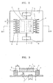
- FIG. 2 is a plan view of the optical scanner of FIG. 1;
- FIG. 3 is a sectional view taken along line III-III of FIG. 2;
- FIG. 4 is a sectional view for explaining an operation of the optical scanner of FIG. 1;
- FIG. 5 is a graph showing a change in frequency when a tuning voltage applied to the tuning electrode of the optical scanner of FIG. 1 is changed;
- FIG. 6 is a perspective view of an optical scanner according to a second arrangement, not an embodiment of the present invention;
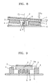
- FIG. 7 is a sectional view taken along line VII-VII of FIG. 6;
- FIG. 8 is a sectional view for explaining an operation of the optical scanner of FIG. 6;
- FIG. 9 is a sectional view of an optical scanner according to a third arrangement, not an embodiment of the present invention;
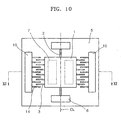
- FIG. 10 is a plan view of an optical scanner according to a fourth arrangement, an embodiment of the present invention;
- FIG. 11 a sectional view taken along line XI-XI of FIG. 10;
- FIG. 12 is a sectional view of an optical scanner according to a fifth arrangement, not an embodiment of the present invention;
- FIG. 13 is a perspective view of an optical scanner according to a sixth arrangement, an embodiment of the present invention;
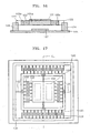
- FIG. 14 is a plan view of the optical scanner of FIG. 13;
- FIG. 15 is a sectional view taken along line X-X of FIG. 14;
- FIG. 16 is a sectional view taken along line Y-Y of FIG. 14; and
- FIG. 17 is a plan view of an optical scanner according to a seventh arrangement, an embodiment of the present invention.
- Referring to FIGS. 1 through 4, in an optical scanner according to a first embodiment of the present invention, a
stage 1a is suspended by a support portion supporting both side ends of thestage 1a above asubstrate 5 made of Pyrex glass. The support portion includes atorsion spring 2 connected to a middle portion of either side edge of thestage 1 a and supporting a seesaw motion of thestage 1a, and ananchor 6 supporting thetorsion spring 2 to be suspended on thesubstrate 5. - A
mirror surface 1 which is an optical scanning surface is formed on an upper surface of thestage 1a. A plurality of drivingcomb electrodes 3 are formed at both sides of thestage 1a to have a predetermined length and parallel to one another. - A plurality of
fixed comb electrodes 4 disposed to alternate with the drivingcomb electrodes 3 are formed on an upper surface of thesubstrate 5 to have a predetermined height and parallel to one another. The drivingcomb electrodes 3 formed on a lower surface of thestage 1a and the fixedcomb electrodes 4 corresponding thereto are dividedly arranged at both sides divided by the center line CL. Atuning electrode 7 is arranged at either side of an area corresponding to thestage 1a with respect to the center line CL. - According to the above structure, the
stage 1a performs a seesaw motion by an electrostatic force between the drivingcomb electrodes 3 and the fixedcomb electrodes 4 are dividedly arranged at both sides with respect to the center line CL. For example, when a predetermined voltage Vd1 is applied to thefixed comb electrodes 4 disposed at the left side with respect to the center line CL, an electrostatic force is generated between thedriving comb electrodes 3 and thefixed comb electrodes 4 so that the drivingcomb electrodes 3 are driven. Thus, thestage 1a is moved downward at the left side. When a predetermined voltage Vd2 is applied to thefixed comb electrodes 4 disposed at the right side with respect to the center line CL as shown in FIG. 4, an electrostatic force is generated between thedriving comb electrodes 3 and thefixed comb electrodes 4 so that thedriving comb electrodes 3 are driven. Thus, thestage 1a is moved downward at the right side. Thestage 1a is returned to the original state by a restoration force according to an elastic coefficient of thetorsion spring 2. The electrostatic force is alternately generated by alternately applying a driving voltage to the fixedcomb electrodes 4 at the left and right sides so that a seesaw motion of thestage 1a is generated. In a state in which thestage 1a is excited at a resonant frequency, when a predetermined voltage Vt is applied to thetuning electrode 7, the resonant frequency of thestage 1a can be controlled. - Next, the principle of tuning the resonant frequency by applying a voltage to the tuning electrode of the optical scanner having the above structure is described below.
- When a predetermined voltage Vd2 is applied to the
fixed comb electrodes 4 at one side, the correspondingdriving comb electrodes 3 are moved toward thefixed comb electrodes 4 by the electrostatic force and rotated around the center line CL as shown in FIG. 4. The driving force at this time is shown inEquation 1.
- Here, ε is a dielectric constant, ld is a length of the driving comb electrode, and g is a gap between the driving comb electrode and the fixed comb electrode.
- A rotational equation of the stage by the driving force is shown in
Equation 2.
- Here, l is an inertia moment of the stage, θ is a driving angle, c is a damping constant,

- When a tuning voltage Vt is applied to the
tuning electrode 7, a new tuning force Ft is generated which is expressed inEquation 3.
- Here, l and h are the lengths of both sides of the tuning electrode and d is a height of between the stage and the tuning electrode.
- The rotational torque by a rotational force of the tuning voltage is shown
Equation 4.
- Here, r=I/2.
- When
Equation 3 where a higher degree term having a low level of significance is removed is applied instead of the tuning force Ft inEquation 4, the tuning spring constant can be defined as shown inEquation 5.
- An exciting torque Nt by the tuning voltage is included in a motion equation of
Equation 2, which is shown inEquation 6.
-
Equation 7 is obtained by applyingEquation 4 toEquation 6.
- Thus, when a tuning voltage is applied to the scanner to which a driving voltage is applied, an effective spring constant is shown in
Equation 8.
- The resonant frequency can be defined as
Equation 9.
- Thus, when the tuning voltage Vt is applied to the
tuning electrode 7, the torsion spring constant of the scanner changes as shown inEquation 8. Accordingly, the frequency of the scanner changes as shown inEquation 9. The resonant frequency of the scanner can be tuned by controlling the tuning voltage. - FIG. 5 is a graph showing a change in frequency when the tuning voltage applied to the tuning electrode of the optical scanner of FIG. 1 is changed. A scanner to be used in a test has a size such that d=30 µm, a size of a mirror is 700x500 µm, a width of the comb electrode is 2 µm, ld= 250 µm, and g=3 µm.
- The spring constant

- When tuning voltages 100 V, 200 V, and 300 V are applied, the effective spring constant by
Equation 8 changes. Accordingly, the resonant frequency changes as shown in FIG. 5, that is, as the tuning voltage Vt increases, the resonant frequency greatly decreases. A desired amount of the decrease in the resonant frequency is 89 Hz. As a result of plotting in FIG. 5, it can be seen that the desired resonant frequency decrease is obtained at the tuning voltage of 170 V. - FIG. 6 is a perspective view of an optical scanner according to a second arrangement, not an embodiment. FIG. 7 is a sectional view taken along line VII-VII of FIG. 6. FIG. 8 is a sectional view for explaining an operation of the optical scanner of FIG. 6. The same reference numerals are used for the same constituent elements as those described in the first embodiment and detailed descriptions thereof will be omitted herein.
- Referring to FIGS. 6 through 8, a plurality of the driving
comb electrodes 3 are formed on the lower portion of thestage 1a to a predetermined height and parallel to one another. The drivingcomb electrodes 3 are dividedly arranged at both sides of the lower portion of thestage 1 a with respect to the center line CL. - A plurality of the fixed
comb electrodes 4 alternating with the drivingcomb electrodes 3 are formed on the upper portion of thesubstrate 5 to a predetermined height and parallel to one another. The fixedcomb electrodes 4 are dividedly arranged at both sides of the upper portion of thesubstrate 5 with respect to the center line CL to correspond to the drivingcomb electrodes 3. - A fixed comb electrode for tuning 8 is arranged at the center portion of the
substrate 5 in the same direction as the center line CL. A driving comb electrode for tuning 9 is arranged on the lower portion of thestage 1a to correspond to the fixed comb electrode fortuning 8. - According to the above structure, the
stage 1a performs a seesaw motion by an electrostatic force between the drivingcomb electrodes 3 and the fixedcomb electrodes 4 disposed at both sides divided by the center line CL. When a predetermined tuning voltage is applied to the fixed comb electrode fortuning 9, a tuning force is generated between the driving comb electrode fortuning 9 and the fixed comb electrode fortuning 8. As the constant of thetorsion spring 2 changes, the driving frequency decreases. Thus, the resonant frequency of the scanner can be controlled by adjusting the tuning voltage. - FIG. 9 is a sectional view of an optical scanner according to a third arrangement, not an embodiment. The same reference numerals are used for the same constituent elements described in the previous arrangements and detailed descriptions thereof will be omitted herein.
- Referring to FIG. 9, the structure of the scanner according to the third arrangement is similar to the scanner according to the first embodiment. However,
electrodes stage 1a and the upper portion of thesubstrate 5. The driving comb electrode for tuning 9 on the lower portion of thestage 1a and the fixed comb electrode for tuning 8 on the upper portion of thesubstrate 5 are installed to alternate with one another. When a tuning voltage is applied to the fixed comb electrode for tuning 8 during the driving of thestage 1a, a tuning force is generated between the drivingcomb electrode 9 and the fixed comb electrode fortuning 8. As described above, the constant of thetorsion spring 2 changes, the resonant frequency decreases. Thus, the resonant frequency of the scanner can be controlled by adjusting the tuning voltage. - FIG. 10 is a plan view of an optical scanner according to a fourth arrangement, an embodiment of the present invention. FIG. 11 a sectional view taken along line XI-XI of FIG. 10. Since the same reference numerals are used for the same constituent elements as those of the first embodiment, detailed descriptions thereof will be omitted herein.
- Referring to FIGS. 10 and 11, the structure of the scanner according to the fourth embodiment is similar to that of the scanner according to the first embodiment. However, a plurality of fixed
comb electrodes 14 to drive thestage 1a are horizontally fixed to ananchor portion 10 fixed on thesubstrate 5. - According to the above structure, the
stage 1a performs a seesaw motion by an electrostatic force between the drivingcomb electrodes 3 and the fixedcomb electrodes 14 disposed at both sides with respect to the center line CL. For example, when a predetermined driving voltage is applied to the fixedcomb electrodes 14 disposed at the left side of the center line CL, an electrostatic force is generated between the drivingcomb electrodes 3 and the fixedcomb electrodes 14 so that the drivingcomb electrodes 3 are driven. Thus, thestage 1a is moved downward at the left side. When a predetermined voltage is applied to thetuning electrode 7, a torsion spring constant changes so that the resonant frequency of the stage can be controlled. - FIG. 12 is a side sectional view of an optical scanner according to a fifth arrangement, not an embodiment of the present invention. Since the same reference numerals are used for the same constituent elements as those of the fourth embodiment, detailed descriptions thereof will be omitted herein.
- Referring to FIG. 12, in the scanner according to the fifth embodiment, the fixed
comb electrodes 14 to drive thestage 1a are horizontally fixed to theanchor portion 10 fixed on thesubstrate 5. The electrodes for tuning the resonant frequency of the scanner are vertically formed on the lower portion of thestage 1a and the upper portion of thesubstrate 5. The drivingcomb electrodes 9 for tuning on the lower portion of thestage 1a and the fixed comb electrode for tuning 8 are installed to be alternate with one another. When a tuning voltage is applied to the fixed comb electrodes for tuning 8 during the driving of thestage 1a, a tuning force is generated between the drivingcomb electrodes 9 for tuning and the fixed comb electrodes fortuning 8. Accordingly, the constant of thetorsion spring 2 changes so that the driving frequency decreases. Thus, the resonant frequency of the scanner can be controlled by adjusting the tuning voltage. - FIG. 13 is a perspective view of an optical scanner according to a sixth arrangement, an embodiment of the present invention. FIG. 14 is a plan view of the optical scanner of FIG. 13. FIGS. 15 and 16 are sectional views taken along line X-X of FIG. 14 and line Y-Y of FIG. 14, respectively.
- Referring to FIGS. 13 through 16, a
stage 101 a having amirror surface 101 formed on an upper surface thereof is supported by a first support portion including afirst torsion spring 102 and arectangular motion frame 120, so as to be able to perform a seesaw motion in a first direction (a direction X) with respect to a center line CL as a center shaft. The first support portion supporting thestage 101a is supported by a second support portion including asecond torsion spring 122 and afixed anchor 130, so as to be able to perform a seesaw motion in a second direction (a direction Y). Thus, thestage 1a supported by the first and second support portions can rotate in two axial directions. - The
rectangular motion frame 120 has afirst portion 120X extending parallel to an axis X, in which thefirst torsion spring 102 is connected in the middle thereof, and asecond portion 120Y extending parallel to an axis Y, in which thesecond torsion spring 122 is connected in the middle thereof. - The
stage 101a is supported and connected to therectangular motion frame 120 by thefirst torsion spring 102 disposed on the axis Y. Thetorsion spring 102 is connected to the middle portion of the opposite edges of thestage 101a. - A plurality of first driving
comb electrodes 103 are formed at both sides of thestage 101a. A plurality of firstfixed comb electrodes 104 arranged to be alternate with the firstdriving comb electrodes 103 are formed on thesecond portion 120Y to be inside theframe 120 and correspond to the firstdriving comb electrodes 103. The drivingcomb electrodes 103 and the fixedcomb electrodes 104 which are symmetrically arranged at both side with respect to thetorsion spring 102 form a stage driving portion. - A motion frame driving portion to seesaw the
stage 101a and themotion frame 120 supporting thestage 101a in the direction Y has a plurality of seconddriving comb electrodes 123 formed outwardly on both sides of themotion frame 120 and a plurality of secondfixed comb electrodes 124 disposed to be alternate with the drivingcomb electrodes 123 and fixed on an upper surface of thesubstrate 105. - A
tuning electrode 107 having a flat panel shape is formed at both sides divided by a line Y-Y in an area of thesubstrate 105 corresponding to thestage 101a. In the above two-axis driving scanner, when thestage 101a rotates in the first direction (the direction x) by an electrostatic force between the firstdriving comb electrode 103 and the firstfixed comb electrode 104, the resonant frequency is tunable by thetuning electrode 107. Meanwhile, thestage 101a is linearly driven in the second direction (the direction Y) by an electrostatic force between the seconddriving comb electrode 123 and the secondfixed comb electrode 124. - FIG. 17 is a plan view of an optical scanner according to a seventh arrangement, an embodiment of the present invention. Since the same reference numerals are used for the same constituent elements as those of the sixth embodiment, detailed descriptions thereof will be omitted herein.
- Referring to FIG. 17, a rectangular fixed
frame 140 supporting thesecond torsion spring 122 and the secondfixed comb electrode 124 is arranged on thesubstrate 105. The secondfixed comb electrode 124 is fixed to an inner side of the rectangular fixedframe 140 so as to be separated from thesubstrate 105. - Since the operation of the optical scanner according to the seventh embodiment is similar to the optical scanner according to the sixth embodiment, a detailed description thereof will be omitted herein.
Claims (12)
- A one-axis or two-axis driving optical scanner comprising:a substrate (5, 105);a stage (1a, 101a) separated from the substrate to a predetermined height and having an upper surface where an optical scanning surface (1) is formed;at least one torsion spring (2, 102, 122) supporting the stage from middle portions of both edge sides of the stage;a support portion (6, 130, 124) fixed to the substrate to support the torsion spring;a driving portion having a plurality of driving comb electrodes (3, 103, 123) extending from the stage and a plurality of fixed comb electrodes (4, 104, 124) arranged to rotate the stage with respect to the torsion spring forming a center axis when a voltage is applied;characterised by further comprising a flat panel type tuning electrode (7) arranged at the centre portion of the substrate in an area of the substrate corresponding to the stage and arranged to change the resonant frequency of rotation of the stage (1a, 101a) of the scanner when a tuning voltage is applied to the tuning electrode wherein the tuning electrode (7) is a plurality of electrodes arranged symmetrically with respect to the center axis.
- The optical scanner as claimed in claim 1, wherein:the plurality of driving comb electrodes (3, 103, 123) extend outwardly from both side surfaces of the stage; andthe plurality of fixed comb electrodes (4, 104, 124) fixed on the substrate to be alternate between the driving comb electrodes.
- The optical scanner as claimed in claim 2, wherein the fixed comb electrodes (4, 104, 124) are vertically arranged on the substrate.
- The optical scanner as claimed in claim 2, wherein the driving portion further comprises an anchor portion (10) separated in a predetermined distance from both sides of the stage (1 a) and fixed on the substrate (5), and the fixed comb electrodes are horizontally extended from the anchor portion.
- A one-axis driving optical scanner according to any preceding claim wherein the tuning electrode includes:at least one driving comb electrode (9) for tuning formed on a lower surface of the stage (1a) to a predetermined height in a direction along the center axis; andat least one fixed comb electrode (8) for tuning formed on the substrate (6) to a predetermined height to be alternate with the driving comb electrode for tuning.
- The optical scanner as claimed in claim 5, wherein the driving portion comprises:a plurality of driving comb electrodes (3) extended from both side surfaces of the center axis on the lower surface of the stage to a predetermined length downward in a direction perpendicular to the center axis; anda plurality of fixed comb electrodes (14) fixed on the substrate to be alternate with the driving comb electrodes.
- A two-axis driving optical scanner according to claim 1, wherein:the stage (101a) is arranged to be driven in a first direction with respect to a center axis in a second direction perpendicular to the first direction;further comprising a first support portion including first torsion springs (102) extending in the second direction from both sides of the stage and a rectangular motion frame (170) having a pair of first portions parallel to each other and respectively connected to the first torsion springs (102) and a pair of second portions parallel to each other and extending in the second direction;wherein the stage driving portion includes a plurality of first fixed comb electrodes (103) and a plurality of first driving comb electrodes (104) formed on inner sides of the second portions and sides of the stage facing the inner sides of the second portions, respectively;
the optical scanner further comprising a second support portion (130, 140) including second torsion springs (122) extending in the first direction from the second portions, the second torsion springs being fixed to the substrate (6); and
a motion frame driving portion including a plurality of second driving comb electrodes (123) provided at outer sides of the first portions and a plurality of second fixed comb electrodes (124) fixed to correspond to the second driving comb electrodes to rotate the motion frame (170) in the second direction. - The optical scanner as claimed in claim 7, wherein the tuning electrode (107) is a plurality of electrodes symmetrically arranged with respect to the center axis.
- The optical scanner as claimed in claim 7 or 8, wherein the second fixed comb electrodes (124) are fixed on the substrate and alternately arranged between the second driving comb electrodes (173).
- The optical scanner as claimed in claim 9, wherein the second fixed comb electrodes (124) are vertically arranged on the substrate (105).
- The optical scanner as claimed in claim 9, wherein the second support portion further comprises an anchor portion (130) fixed on the substrate and separated in a predetermined distance from the second portion of the motion frame, and the second fixed comb electrodes (124) are horizontally extended from the anchor portion.
- The optical scanner as claimed in any of claims 7 to 11, wherein the second support portion (140) comprises a rectangular frame which fixes the second comb electrodes and the second torsion springs therein.
Applications Claiming Priority (2)
| Application Number | Priority Date | Filing Date | Title |
|---|---|---|---|
| KR2003074662 | 2003-10-24 | ||
| KR1020030074662A KR100940206B1 (en) | 2003-10-24 | 2003-10-24 | Frequency modulated resonant scanner |
Publications (2)
| Publication Number | Publication Date |
|---|---|
| EP1526399A1 EP1526399A1 (en) | 2005-04-27 |
| EP1526399B1 true EP1526399B1 (en) | 2007-08-15 |
Family
ID=34386804
Family Applications (1)
| Application Number | Title | Priority Date | Filing Date |
|---|---|---|---|
| EP04256467A Expired - Lifetime EP1526399B1 (en) | 2003-10-24 | 2004-10-20 | Frequency tunable resonant scanner |
Country Status (5)
| Country | Link |
|---|---|
| US (2) | US7242511B2 (en) |
| EP (1) | EP1526399B1 (en) |
| JP (1) | JP4012535B2 (en) |
| KR (1) | KR100940206B1 (en) |
| DE (1) | DE602004008182T2 (en) |
Families Citing this family (26)
| Publication number | Priority date | Publication date | Assignee | Title |
|---|---|---|---|---|
| KR100486716B1 (en) * | 2002-10-18 | 2005-05-03 | 삼성전자주식회사 | 2-dimensional actuator and manufacturing method thereof |
| TWI235735B (en) * | 2004-06-18 | 2005-07-11 | Walsin Lihwa Corp | Two-axis element and manufacturing method thereof |
| JP2006053396A (en) * | 2004-08-12 | 2006-02-23 | Tohoku Univ | Drive mechanism and micromirror device provided with the mechanism |
| KR100695153B1 (en) * | 2005-06-15 | 2007-03-14 | 삼성전자주식회사 | Actuator with vertical comb electrode |
| CN101268400A (en) | 2005-09-21 | 2008-09-17 | 松下电器产业株式会社 | actuator |
| JP4734122B2 (en) * | 2006-01-16 | 2011-07-27 | 富士フイルム株式会社 | Light modulation element, actuator, and driving method of actuator |
| JP4765840B2 (en) * | 2006-08-28 | 2011-09-07 | パナソニック電工株式会社 | Tilt mirror element |
| JP2008116699A (en) | 2006-11-06 | 2008-05-22 | Sony Corp | Drive element |
| JP5309441B2 (en) * | 2006-11-16 | 2013-10-09 | 株式会社デンソー | Two-dimensional optical scanning device |
| KR101177167B1 (en) | 2006-12-12 | 2012-08-24 | 엔엑스피 비 브이 | Mems device with controlled electrode off-state position |
| DE102007001516B3 (en) * | 2007-01-10 | 2008-04-30 | Fraunhofer-Gesellschaft zur Förderung der angewandten Forschung e.V. | Micromechanical unit for e.g. use in light deflector, has resonance frequency adjusting device adjusting resonance frequency of oscillation system such that positions of spring hangers of hanger assembly are changed to one another |
| EP2280906A4 (en) | 2008-04-29 | 2013-10-23 | Micralyne Inc | Mems device with independent rotation in two axes of rotation |
| JP5458837B2 (en) | 2009-03-16 | 2014-04-02 | 株式会社リコー | Optical scanning device |
| CN102369153B (en) * | 2009-03-31 | 2014-12-31 | 富士通株式会社 | Micro movable element array and communication apparatus |
| EP2302712A1 (en) * | 2009-09-28 | 2011-03-30 | Stichting IMEC Nederland | Method for resonance frequency tuning of micromachined structures |
| EP2526453A1 (en) * | 2010-01-22 | 2012-11-28 | Cambridge Technology, Inc. | Low wobble wide scan angle taut-band resonant scanners with matched coefficients of thermal expansion and interchangeable mirrors |
| CN102311090B (en) * | 2010-07-02 | 2014-04-30 | 先进微系统科技股份有限公司 | Two-dimensional comb actuator and manufacturing method thereof |
| WO2012095185A1 (en) * | 2011-01-14 | 2012-07-19 | Fraunhofer-Gesellschaft zur Förderung der angewandten Forschung e.V. | Micromechanical component |
| JP5846097B2 (en) * | 2012-10-29 | 2016-01-20 | 株式会社デンソー | Optical scanning device |
| JP5664711B2 (en) * | 2013-06-21 | 2015-02-04 | セイコーエプソン株式会社 | Actuator, optical scanner, and image forming apparatus |
| DE102013212095B4 (en) * | 2013-06-25 | 2024-06-27 | Robert Bosch Gmbh | Micro-electromechanical reflector and method for producing a micro-electromechanical reflector |
| DE102013223937B4 (en) * | 2013-11-22 | 2022-01-05 | Fraunhofer-Gesellschaft zur Förderung der angewandten Forschung e.V. | Micromirror array |
| TWI621582B (en) * | 2015-08-14 | 2018-04-21 | 先進微系統科技股份有限公司 | Comb-shaped actuator |
| US20210139314A1 (en) * | 2019-11-07 | 2021-05-13 | Innovative Interface Laboratory Corp. | Linear actuator |
| CN115980928A (en) * | 2023-01-16 | 2023-04-18 | 上海镭望光学科技有限公司 | Optical switch and optical switch array |
| DE102023102347A1 (en) * | 2023-01-31 | 2024-08-01 | Carl Zeiss Smt Gmbh | Optical component |
Family Cites Families (13)
| Publication number | Priority date | Publication date | Assignee | Title |
|---|---|---|---|---|
| US5914553A (en) * | 1997-06-16 | 1999-06-22 | Cornell Research Foundation, Inc. | Multistable tunable micromechanical resonators |
| JP3011144B2 (en) * | 1997-07-31 | 2000-02-21 | 日本電気株式会社 | Optical scanner and its driving method |
| US6285489B1 (en) * | 1999-08-05 | 2001-09-04 | Microvision Inc. | Frequency tunable resonant scanner with auxiliary arms |
| KR100486704B1 (en) * | 1999-11-05 | 2005-05-03 | 삼성전자주식회사 | Optical scanner and laser image projector adopting the same and driving method of the projector |
| JP2001194151A (en) | 2000-01-07 | 2001-07-19 | Murata Mfg Co Ltd | Resonant element |
| KR100400218B1 (en) | 2000-08-18 | 2003-10-30 | 삼성전자주식회사 | micro-actuator and manufacturing method therof |
| JP2002148554A (en) | 2000-11-03 | 2002-05-22 | Samsung Electronics Co Ltd | Optical scanner, laser image projection apparatus using the same, and method of driving the same |
| JP3908566B2 (en) | 2001-03-02 | 2007-04-25 | 三星電子株式会社 | Micromirror drive device and control method thereof |
| KR100788644B1 (en) * | 2001-03-02 | 2007-12-26 | 삼성전자주식회사 | Micromirror Drive |
| KR100434541B1 (en) * | 2001-08-24 | 2004-06-05 | 삼성전자주식회사 | Optical scanner and manufacturing method thereof |
| US6769616B2 (en) * | 2002-11-22 | 2004-08-03 | Advanced Nano Systems | Bidirectional MEMS scanning mirror with tunable natural frequency |
| US7034370B2 (en) * | 2002-11-22 | 2006-04-25 | Advanced Nano Systems, Inc. | MEMS scanning mirror with tunable natural frequency |
| US7042613B2 (en) * | 2003-08-12 | 2006-05-09 | Terraop Ltd. | Bouncing mode operated scanning micro-mirror |
-
2003
- 2003-10-24 KR KR1020030074662A patent/KR100940206B1/en not_active Expired - Fee Related
-
2004
- 2004-10-14 US US10/963,693 patent/US7242511B2/en not_active Expired - Fee Related
- 2004-10-20 DE DE602004008182T patent/DE602004008182T2/en not_active Expired - Lifetime
- 2004-10-20 EP EP04256467A patent/EP1526399B1/en not_active Expired - Lifetime
- 2004-10-22 JP JP2004308316A patent/JP4012535B2/en not_active Expired - Fee Related
-
2007
- 2007-06-05 US US11/806,946 patent/US7436574B2/en not_active Expired - Fee Related
Non-Patent Citations (1)
| Title |
|---|
| None * |
Also Published As
| Publication number | Publication date |
|---|---|
| US7436574B2 (en) | 2008-10-14 |
| JP4012535B2 (en) | 2007-11-21 |
| EP1526399A1 (en) | 2005-04-27 |
| DE602004008182T2 (en) | 2008-04-30 |
| KR100940206B1 (en) | 2010-02-10 |
| US7242511B2 (en) | 2007-07-10 |
| DE602004008182D1 (en) | 2007-09-27 |
| JP2005128551A (en) | 2005-05-19 |
| KR20050039232A (en) | 2005-04-29 |
| US20050088720A1 (en) | 2005-04-28 |
| US20070236767A1 (en) | 2007-10-11 |
Similar Documents
| Publication | Publication Date | Title |
|---|---|---|
| US7436574B2 (en) | Frequency tunable resonant scanner | |
| US20050099665A1 (en) | Frequency tunable resonant scanner | |
| JP4385938B2 (en) | Actuator | |
| US8345336B2 (en) | MEMS scanning micromirror with reduced dynamic deformation | |
| TWI446000B (en) | Mems scanning micromirror | |
| KR100908187B1 (en) | Micro rocking element | |
| KR100682958B1 (en) | 2-axis micro scanner | |
| EP2769256B1 (en) | Mems scanning micromirror | |
| US6765711B2 (en) | Micromirror driver and method of controlling micromirror driver | |
| US5959760A (en) | Light beam scanner using large electrostatic force | |
| CN100360984C (en) | Rotary-type comb-drive actuator and variable optical attenuator using the same | |
| KR20120024647A (en) | Micromechanical component and production method for a micromechanical component | |
| JP2012510254A (en) | Electrostatic comb micro-mechanical actuator | |
| JP4098792B2 (en) | Mirror device | |
| US20150002916A1 (en) | Mems device and methods for manufacturing and using same | |
| EP2245496A1 (en) | Oscillating structure and oscillator device using the same | |
| JP2006167860A (en) | Actuator | |
| JP4123133B2 (en) | Actuator | |
| JP2013186224A (en) | Optical reflection element | |
| EP4446794B1 (en) | Two-axis mems mirror | |
| EP4564077A1 (en) | Quasi-static actuation of a mems mirror | |
| KR20060100146A (en) | Actuator with multi-layer plate structure |
Legal Events
| Date | Code | Title | Description |
|---|---|---|---|
| PUAI | Public reference made under article 153(3) epc to a published international application that has entered the european phase |
Free format text: ORIGINAL CODE: 0009012 |
|
| 17P | Request for examination filed |
Effective date: 20041110 |
|
| AK | Designated contracting states |
Kind code of ref document: A1 Designated state(s): AT BE BG CH CY CZ DE DK EE ES FI FR GB GR HU IE IT LI LU MC NL PL PT RO SE SI SK TR |
|
| AX | Request for extension of the european patent |
Extension state: AL HR LT LV MK |
|
| AKX | Designation fees paid |
Designated state(s): DE FR GB |
|
| GRAP | Despatch of communication of intention to grant a patent |
Free format text: ORIGINAL CODE: EPIDOSNIGR1 |
|
| GRAS | Grant fee paid |
Free format text: ORIGINAL CODE: EPIDOSNIGR3 |
|
| GRAA | (expected) grant |
Free format text: ORIGINAL CODE: 0009210 |
|
| AK | Designated contracting states |
Kind code of ref document: B1 Designated state(s): DE FR GB |
|
| REG | Reference to a national code |
Ref country code: GB Ref legal event code: FG4D |
|
| REF | Corresponds to: |
Ref document number: 602004008182 Country of ref document: DE Date of ref document: 20070927 Kind code of ref document: P |
|
| ET | Fr: translation filed | ||
| PLBE | No opposition filed within time limit |
Free format text: ORIGINAL CODE: 0009261 |
|
| STAA | Information on the status of an ep patent application or granted ep patent |
Free format text: STATUS: NO OPPOSITION FILED WITHIN TIME LIMIT |
|
| 26N | No opposition filed |
Effective date: 20080516 |
|
| PGFP | Annual fee paid to national office [announced via postgrant information from national office to epo] |
Ref country code: FR Payment date: 20131015 Year of fee payment: 10 Ref country code: GB Payment date: 20131011 Year of fee payment: 10 Ref country code: DE Payment date: 20131015 Year of fee payment: 10 |
|
| REG | Reference to a national code |
Ref country code: DE Ref legal event code: R119 Ref document number: 602004008182 Country of ref document: DE |
|
| GBPC | Gb: european patent ceased through non-payment of renewal fee |
Effective date: 20141020 |
|
| PG25 | Lapsed in a contracting state [announced via postgrant information from national office to epo] |
Ref country code: GB Free format text: LAPSE BECAUSE OF NON-PAYMENT OF DUE FEES Effective date: 20141020 Ref country code: DE Free format text: LAPSE BECAUSE OF NON-PAYMENT OF DUE FEES Effective date: 20150501 |
|
| REG | Reference to a national code |
Ref country code: FR Ref legal event code: ST Effective date: 20150630 |
|
| PG25 | Lapsed in a contracting state [announced via postgrant information from national office to epo] |
Ref country code: FR Free format text: LAPSE BECAUSE OF NON-PAYMENT OF DUE FEES Effective date: 20141031 |