EP1525779B1 - Driver for a gas discharge lamp - Google Patents
Driver for a gas discharge lamp Download PDFInfo
- Publication number
- EP1525779B1 EP1525779B1 EP03740927A EP03740927A EP1525779B1 EP 1525779 B1 EP1525779 B1 EP 1525779B1 EP 03740927 A EP03740927 A EP 03740927A EP 03740927 A EP03740927 A EP 03740927A EP 1525779 B1 EP1525779 B1 EP 1525779B1
- Authority
- EP
- European Patent Office
- Prior art keywords
- current
- output
- input
- coupled
- commutation
- Prior art date
- Legal status (The legal status is an assumption and is not a legal conclusion. Google has not performed a legal analysis and makes no representation as to the accuracy of the status listed.)
- Expired - Lifetime
Links
- 230000003247 decreasing effect Effects 0.000 claims abstract description 6
- 238000004804 winding Methods 0.000 claims description 29
- 229920006395 saturated elastomer Polymers 0.000 claims description 4
- 230000001360 synchronised effect Effects 0.000 abstract 1
- 238000013461 design Methods 0.000 description 14
- 238000010586 diagram Methods 0.000 description 8
- 230000008901 benefit Effects 0.000 description 7
- 230000007423 decrease Effects 0.000 description 7
- 230000000630 rising effect Effects 0.000 description 6
- 239000003990 capacitor Substances 0.000 description 4
- 230000008859 change Effects 0.000 description 4
- 238000001514 detection method Methods 0.000 description 4
- 230000007704 transition Effects 0.000 description 4
- 230000001960 triggered effect Effects 0.000 description 4
- 230000000694 effects Effects 0.000 description 2
- 230000004044 response Effects 0.000 description 2
- 238000013459 approach Methods 0.000 description 1
- 230000003111 delayed effect Effects 0.000 description 1
- 238000002474 experimental method Methods 0.000 description 1
- 230000004907 flux Effects 0.000 description 1
- 239000000463 material Substances 0.000 description 1
- 238000005259 measurement Methods 0.000 description 1
- 238000012986 modification Methods 0.000 description 1
- 230000004048 modification Effects 0.000 description 1
- 230000035699 permeability Effects 0.000 description 1
- 230000001681 protective effect Effects 0.000 description 1
- 238000011084 recovery Methods 0.000 description 1
- 230000001131 transforming effect Effects 0.000 description 1
- 229910000859 α-Fe Inorganic materials 0.000 description 1
Images


Classifications
-
- H—ELECTRICITY
- H05—ELECTRIC TECHNIQUES NOT OTHERWISE PROVIDED FOR
- H05B—ELECTRIC HEATING; ELECTRIC LIGHT SOURCES NOT OTHERWISE PROVIDED FOR; CIRCUIT ARRANGEMENTS FOR ELECTRIC LIGHT SOURCES, IN GENERAL
- H05B41/00—Circuit arrangements or apparatus for igniting or operating discharge lamps
- H05B41/14—Circuit arrangements
- H05B41/26—Circuit arrangements in which the lamp is fed by power derived from dc by means of a converter, e.g. by high-voltage dc
- H05B41/28—Circuit arrangements in which the lamp is fed by power derived from dc by means of a converter, e.g. by high-voltage dc using static converters
- H05B41/282—Circuit arrangements in which the lamp is fed by power derived from dc by means of a converter, e.g. by high-voltage dc using static converters with semiconductor devices
- H05B41/2825—Circuit arrangements in which the lamp is fed by power derived from dc by means of a converter, e.g. by high-voltage dc using static converters with semiconductor devices by means of a bridge converter in the final stage
- H05B41/2828—Circuit arrangements in which the lamp is fed by power derived from dc by means of a converter, e.g. by high-voltage dc using static converters with semiconductor devices by means of a bridge converter in the final stage using control circuits for the switching elements
-
- Y—GENERAL TAGGING OF NEW TECHNOLOGICAL DEVELOPMENTS; GENERAL TAGGING OF CROSS-SECTIONAL TECHNOLOGIES SPANNING OVER SEVERAL SECTIONS OF THE IPC; TECHNICAL SUBJECTS COVERED BY FORMER USPC CROSS-REFERENCE ART COLLECTIONS [XRACs] AND DIGESTS
- Y10—TECHNICAL SUBJECTS COVERED BY FORMER USPC
- Y10S—TECHNICAL SUBJECTS COVERED BY FORMER USPC CROSS-REFERENCE ART COLLECTIONS [XRACs] AND DIGESTS
- Y10S315/00—Electric lamp and discharge devices: systems
- Y10S315/07—Starting and control circuits for gas discharge lamp using transistors
Landscapes
- Circuit Arrangements For Discharge Lamps (AREA)
- Inverter Devices (AREA)
Abstract
Description
- The present invention relates in general to drivers for gas discharge lamps. As is commonly known, a driver for a gas discharge lamp serves to feed the gas discharge lamp with the required amount of current, and receives power itself from AC mains. Conventionally, such a driver comprises three stages: a rectifier and upconverter for converting the AC input voltage to a higher DC output voltage, a downconverter for converting said DC voltage to a lower voltage but higher current, and finally a commutator switching the DC current for the lamp at a relatively low frequency. In a more recent design, the last two stages (i.e. downconverter and commutator) have been integrated into a single stage, referred to as forward commutating stage. Such an integrated stage offers advantages, such as fewer components and a smaller size.
- In such a forward commutating stage, one can distinguish between a half-bridge type and a full-bridge type. However, such a forward commutating stage always has at least one chain of two series-connected MOSFET switches, wherein the gas discharge lamp to be driven is connected to the node between said two switches.
- During steady state operation, the lamp current in principle has a substantially constant magnitude, but the lamp current changes direction at regular intervals. A full lamp period comprises a first time interval where the lamp current has one direction, and a second time interval where the lamp current has the reverse direction. During each of these intervals, one of said two chain switches is active, while the other is passive. Conventionally, the active switch is switched open (non-conductive state) and closed (conductive state) at a relatively high frequency. During the closed condition of this active switch, current for a lamp circuit is conducted by this active switch and increases in magnitude. During the open condition of this active switch, the lamp circuit current is conducted by a diode in parallel with the other switch, i.e. the passive switch. This diode may be the internal body diode of the MOSFET switch itself. However, this internal body diode behaves badly at relatively high frequencies, especially at the transition from the conductive state to the non-conductive state, which causes relatively much loss of energy. In order to improve this switching behavior, it has already been proposed to add two separate diodes for each MOSFET switch, one diode being series-connected and the other being anti-parallel connected. Then, when the active MOSFET is opened, the lamp circuit current is conducted by said anti-parallel diode, while said series-connected diode blocks the current through said passive switch. However, this design involves two additional components for each MOSFET, while additionally the series-connected diode contributes to energy losses when its corresponding MOSFET is the active MOSFET.
- It is a general objective of the present invention to provide an improved driver for a gas discharge lamp. Particularly, it is an objective of the present invention to provide an improved forward commutator device for a gas discharge lamp.
- In a first aspect, the present invention is based on the recognition that a MOSFET switch can conduct current in two directions. The present invention utilizes this recognition by using the passive MOSFET itself for conducting the lamp circuit current during those moments that the active MOSFET is open.
- It is noted that
US patent 5,932,976 discloses a driver for a gas discharge lamp, where in a first phase the lamp is driven with a relatively high frequency while in a second phase the lamp is driven with a relatively low frequency. However, in that prior art circuit the first phase is a start-up phase while the second phase is normal operation. During normal operation, in each of the commutation intervals, the lamp is driven with the same frequency. Further, while the active switch is being switched, the passive switch is kept non-conductive. - Conventionally, the active MOSFET is closed (i.e.: switched to its conductive state, also indicated as the ON state) when the decreasing lamp circuit current reaches a first current level, and this active MOSFET is opened (i.e.: switched to its non-conductive state, also indicated as the OFF state) when the increasing lamp circuit current through the active MOSFET reaches a second, higher current level. Conventionally, the first current level is higher than zero. However, it is advantageous if the active MOSFET would be switched ON at approximately zero lamp current, because then switching losses are minimal. This is especially the case when, in accordance with the above-mentioned first aspect of the present invention, the passive MOSFET is switched ON when the active MOSFET is switched OFF. Thus, there is a need for an accurate current sensor which accurately indicates zero-crossings of the lamp circuit current. It is, of course, possible to use a measuring resistor in series with the lamp circuit current and to measure the voltage across this measuring resistor, but this will involve relatively large resistive losses.
- Therefore, it is a further objective of the present invention to provide a relatively simple, accurate current sensor which involves relatively little losses.
- Ideally, switching takes place when the lamp circuit current is exactly zero. However, generating a detector signal, sending this detecting signal to a control device for the MOSFET switches, and switching the MOSFET switches, causes a time delay between the moment of detection and the moment of actual switching. Therefore, it is a further objective to provide a zero crossing detector which can already provide a sensor signal shortly before the actual zero crossing.
- In accordance with a second aspect of the present invention, a zero-crossing current detector comprises a small transformer having a first transformer winding connected in series with the lamp current. The small transformer is already saturated at relatively small primary currents; then, at the secondary side, no signal will be provided. Only at relatively small currents, i.e. around the zero crossings, the transformer is out of saturation and a signal is provided at its secondary winding.
- As mentioned above, the lamp current changes direction at regular intervals. This is referred to as the commutation moment. At the commutation moment, the active MOSFET becomes the passive MOSFET, while the passive MOSFET becomes the active MOSFET. In the state of the art, the commutation moment is determined independently of the actual status of the lamp current. This means that the actual commutation moment is at random with respect to the actual current magnitude, which may lead to undesirable lamp behavior. It is a further objective of the present invention to improve lamp behavior by a better control of the commutation moment. According to a further aspect of the present invention, the commutation moment is selected in synchronization with the high frequency switching of the MOSFET switches. More particularly, the commutation moment is selected to substantially coincide with a zero crossing.
- These and other aspects, features and advantages of the present invention will be further explained by the following description of a preferred embodiment of a driver according to the present invention with reference to the drawings, in which same reference numerals indicate same or similar parts, and in which:
-
Fig. 1A schematically illustrates a conventional driver for a gas discharge lamp; -
Fig. 1 B is a graph illustrating lamp current as a function of time; -
Fig. 2 schematically illustrates another conventional driver for a gas discharge lamp; -
Fig. 3 is a block diagram showing a state of the art commutating forward driver in more detail; -
Fig. 4A is a timing diagram illustrating lamp circuit current and control signals as a function of time; -
Fig. 4B is a timing diagram illustrating lamp current and control signals as a function of time, on a different scale; -
Fig. 5 is a schematic circuit diagram of a driver according to the present invention; -
Fig. 6 is a timing diagram, comparable toFig. 4A , illustrating the lamp circuit current and driver control signals as a function of time for the driver according to the present invention; -
Fig. 7A schematically illustrates a current sensor according to the present invention; -
Fig. 7B is a graph illustrating the performance of the current sensor ofFig. 7A ; -
Fig. 8 is a functional block diagram schematically illustrating an exemplary embodiment of a control unit; -
Fig. 9 is a graph showing lamp circuit current as well as several signals as a function of time. -
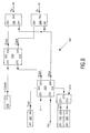
Fig. 1A schematically illustrates aconventional driver 1 for agas discharge lamp 9. Theconventional driver 1 comprises afirst stage 10, also referred to as preconditioner, having aninput 11 for receiving an AC mains voltage, typically in the order of about 230 V. The pre-conditioner 10 comprises rectifying means for rectifying the input voltage, and up-transformer means for transforming the rectified voltage to a higher DC voltage, typically in the order of 400 V or higher. This upconverted DC voltage is provided at anoutput 12 of thepreconditioner 10. Since such preconditioners are commonly known, and the design of such a preconditioner is no subject of the present invention, while a preconditioner that is known per se may be used in the driver according to the present invention, thepreconditioner 10 will not be explained here in more detail. - A conventional driver has a second stage or
downconverter 20, having aninput 21 connected to theoutput 12 of the pre-conditioner 10, and having anoutput 22 providing a DC output current at a voltage level lower than the output voltage of the pre-conditioner 10. In principle, this DC output current of thedownconverter 20 might be provided directly to alamp 9; however, gas discharge lamps need to be driven in general at an alternating current. For this purpose, conventionally acommutator 30 is present, having aninput 31 receiving the DC current generated by thedownconverter 20, and providing an alternating DC current at itsoutput 32.Fig. 1B illustrates schematically the shape of the current IL through thelamp 9 as a function of time t; herein, the superimposed high-frequency ripple components are neglected. During afirst commutation interval 41, the lamp current flows in one direction, whereas in asecond commutation interval 42 the lamp current has the same magnitude but flows in the opposite direction. -
Fig. 2 schematically illustrates a commonly known design for adriver 2, in which the twoseparate stages downconverter 20 and thecommutator 30, have been replaced by one singlecommutating forward device 50, having aninput 51 receiving the DC output voltage of thepreconditioner 10, and having anoutput 52 generating an alternating DC current as generally illustrated inFig. 1B . -
Fig. 3 shows the main components of a state of the art commutating forwarddriver 50 for illustrating the operation thereof. In this example, the commutating forwarddevice 50 is of the half-bridge type; a skilled person will recognize that the following explanation can, mutatis mutandis, be applied also to a commutating forward device of the full-bridge type. - The commutating forward
driver 50, hereinafter abbreviated asCFD 50, has twoinput terminals first input terminal 51a being maintained at a voltage level higher than thesecond input terminal 51b, the voltage difference typically being about 400 V. Furthermore, theCFD 50 has twooutput terminals lamp 9. - A body diode of the
MOSFETS - The
CFD 50 comprises afirst MOSFET switch 61 having its source and drain terminals connected between thefirst input terminal 51a and a first node P, and asecond MOSFET switch 62 having its source and drain terminals connected between said first node P and thesecond input terminal 51b. TheCFD 50 further comprises afirst capacitor 71 connected between thefirst input terminal 51a and a second node Q, and asecond capacitor 72 connected between this second node Q and thesecond input terminal 51b. Between said two nodes P and Q, acoil 73 is connected in series with alamp circuit 99. Lamp output terminals are indicated at 52a and 52b. Saidlamp circuit 99 comprises thelamp 9 arranged in series with an ignitor coil, and a filter capacitor arranged in parallel with said series arrangement. Current applied to saidlamp circuit 99 will be indicated as lamp circuit current ILC. Said ignitor coil and filter capacitor serve to smoothen the current through thelamp 9, indicated as lamp current IL. - Furthermore, the
CFD 50 comprises acontrol unit 80, having afirst output 81 coupled to the gate terminal of thefirst MOSFET 61, and asecond output 82 coupled to the gate terminal of thesecond MOSFET 62. Thecontrol unit 80 is designed to open and close the MOSFET switches 61 and 62 by supplying control signal S1 and S2 at itsoutputs - The operation of the half-
bridge CFD 50 will now be explained, while also referring toFig. 4A , which shows the conventional control signals S1 and S2 and the lamp circuit current ILC as a function of time t. During the first commutation interval 41 (seeFigs. 1B and4B ), twooperational phases operational phase 43, which will also be indicated as themain phase 43, the output control signal S1 at thefirst output terminal 81 of thecontrol unit 80 is such that thefirst MOSFET 61 is in the conductive state, while the second output control signal S2 at thesecond output 82 of thecontrol unit 80 is such that thesecond MOSFET 62 is in the non-conductive state. Then, the lamp circuit current passes from thefirst input terminal 51a through thefirst MOSFET 61, thelamp coil 73 and thelamp circuit 99, as indicated by a first arrow A1. This lamp current increases in magnitude during thisfirst phase 43, as illustrated inFig. 4A . - At a certain switching time tH, the
control unit 80 changes its first output control signal S1 such that the first MOSFET switches to its non-conductive state. At that moment, the lamp circuit current ILC has a certain magnitude, indicated as IHIGH inFig. 4A . The second control output signal S2 is maintained, such that thesecond MOSFET 62 remains in its non-conductive state. Thelamp coil 73, which can be considered as being charged with magnetic energy, now provides for a continuation of the lamp circuit current in the same direction, albeit at a decreasing current magnitude. This current cannot flow from thefirst input terminal 51a, but flows from thesecond input terminal 51b through thelamp coil 73 and thelamp 9. Hereinafter, this current will also be indicated as coil-driven current I44. - At a later moment in time, indicated as tL in
Fig. 4A , thecontrol unit 80 again changes its first output control signal S1 such that thefirst MOSFET 61 is again switched to its conductive state. At that moment, the lamp circuit current has reached a current level ILOW lower than the first level IHIGH. The secondoperational phase 44 between tH and tL, during which the lamp circuit current is coil-driven and decreases from first current level IHIGH to second current level ILOW, will also be indicated as coil-drivenphase 44. - The
first switch 61, which conducts the lamp circuit current during themain phase 43, will also be indicated as the active switch. Theother switch 62 will be indicated as passive switch. - In the state of the art, during the first interval, the
first switch 61 oractive switch 61 is repeatedly switched on and off, while thepassive switch 62 remains switched off. In one possible embodiment of the state of theart CFD 50, the coil-driven current I44 flows through thesecond body diode 64 of the passivesecond MOSFET 62, as indicated inFig. 3 by arrow A2a. - In another possible embodiment of the
prior art CFD 50, a firstexternal diode 91 is connected in series with thefirst MOSFET 61, its anode being coupled to thefirst input terminal 51a and its cathode being coupled to theMOSFET 61. Similarly, asecond diode 92 is connected in series with thesecond MOSFET 62. A thirdexternal diode 93 is connected between thefirst input terminal 51a and the first node P, its cathode being connected tofirst input terminal 51a and its anode being connected to first node P. Similarly, a fourth external diode 94 is connected between first node P andsecond input terminal 51b. In such an embodiment, thesecond diode 92 prevents the flow of coil-driven current throughsecond body diode 64, and the coil-driven current I44 now flows through fourth diode 94, as indicated by arrow A2b. - As discussed in the introduction, both prior art solutions have disadvantages. To complete the description of the operation of
CFD 50, the switching offirst MOSFET 61 is repeated continuously until a commutation moment. At such a moment, thefirst commutation interval 41 ends and thesecond commutation interval 42 starts (seeFigs. 1B and4B ). During thesecond interval 42, thesecond MOSFET 62 is repeatedly switched on and off while thefirst MOSFET 61 is maintained in its off state. It will be clear to a person skilled in the art that now the lamp circuit current flows in the opposite direction through thelamp circuit 99, and rises during a main phase or active phase from a low current magnitude to a high current magnitude and decreases in a coil-driven phase from the high magnitude to the lower magnitude. During the main phase oractive phase 43, the current is conducted by thesecond MOSFET 62, while in the coil-drivenphase 44, the current passes through thefirst body diode 63 of thefirst MOSFET 61 or, alternatively, through the thirdseparate diode 93 parallel to saidfirst MOSFET 61. -
Fig. 4B is a timing diagram of the control output signals of thecontrol unit 80 in relation to theintervals Fig. 1B , according to the state of the art. -
Fig. 5 is a schematic circuit diagram of aCFD 150 according to the present invention, comparable toFig. 3 . As can be seen, the separate diodes 91-94 are not present. However, theCFD 150 according to the present invention does not have the above-mentioned disadvantages of the prior art as regards thebody diodes Fig. 3 ). According to the present invention, however, while the main current flows through theactive switch 61 during themain phase 43, as indicated by arrow A1 inFig. 5 , the coil-driven current I44 flows through the channel of the passivesecond MOSFET 62 during the coil-drivenphase 44, as indicated by arrow A3 inFig. 5 . -
Fig. 6 is a graph, comparable toFig. 4A , illustrating the command output signals S1 and S2 of acontrol unit 180 according to the present invention, as well as the resulting circuit current ILC through thelamp circuit 99, as a function of time. When comparingFig. 6 withFig. 4A , it will be clear that the timing of the control output signal S1, S2 for the active MOSFET, i.e. thefirst MOSFET 61 during thefirst commutation interval 41 and thesecond MOSFET 62 during thesecond commutation interval 42, is the same as in the state of the art. However, in contrast to the state of the art, the passive switch is also switched on and off in counter-phase with the switching of the active switch. - It is noted that this timing as illustrated in
Fig. 6 seems similar to the timing of a synchronic inverter. However, in the case of an inverter, the current through each switch is always directed from drain to source. This means that, if the circuit were driven as an inverter, the control signal S1 would be high during the first commutation interval and the second control signal S2 would be low during the same commutation interval, resulting in a current in the direction from node P to node Q, this current flowing throughfirst switch 61 from its drain terminal to its source terminal, while in the second commutation interval, the first control signal S1 would be low and the second control signal S2 would be high, resulting in a current from node Q to node P, which would flow through the second switch from its drain to its source. However, in the present invention, during the coil-drivenphase 44 of thefirst commutation interval 41, when the first control signal S1 is low and the second control signal S2 is high, the current is still in the direction from node P to node Q, thus flowing through thesecond MOSFET 62 from its source to its drain. - An important advantage obtained by using the low-resistive MOSFET channel for conducting current from source to drain is the fact that switching of the MOSFET is much faster than switching of its body diode. Specifically, the MOSFET can be switched off much faster than its body diode, or much faster than any other diode for that matter, so reversed recovery losses are eliminated.
- The switching principle proposed by the present invention, based on the use of the MOSFET channel from source to drain, can already be used in principle if the second or lower current level ILOW has an arbitrary value above zero. However, full advantage of the inventive idea is achieved if the lower current level ILOW is equal to zero. This mode of operating a gas discharge lamp is indicated as critical discontinuous mode. In order to be able to accurately switch when the lamp-current is close to zero, the
inventive CFD 150 preferably comprises acurrent sensor 100, as illustrated inFig. 5 , which senses the lamp circuit current and sends a detector signal SD to asensor input 183 of thecontrol unit 180, the sensor signal SD being indicative of a zero crossing. -
Fig. 7A illustrates a preferred embodiment of such acurrent sensor 100. Important advantages of this preferred embodiment are the small size, the low number of components, and the low cost. - The preferred embodiment of a
current sensor 100 proposed by the present invention and as illustrated inFig. 7A comprises asmall transformer 110 having a primary winding 111 and a secondary winding 112. The primary winding 111 is connected in series with thelamp circuit 99 between the nodes P and Q, so that the full lamp circuit current ILC passes through this first winding 111. InFig. 5 , the primary winding 111 is connected in series between thecoil 73 and thelamp 9. Afirst diode 113 has its anode connected to a first end of the secondary winding 112, and asecond diode 114 has its anode connected to the other end of the secondary winding 112. The cathodes of these twodiodes resistor 115, the other terminal of said resistor being connected to afirst output terminal 120a of thecurrent sensor 100. Asecond output terminal 120b of thecurrent sensor 100 is connected to a central terminal of the secondary winding 112. - The
transformer 110, preferably of the toroidal type, is very small, so that its core is saturated even at a relatively small current through its primary winding 111. In such a saturated condition, an increase or decrease of the lamp current through primary winding 111 will not result in a change of magnetic flux within this core, and therefore will not result in any current in the secondary winding 112. However, as soon as the current through the primary winding 111 approaches zero, thetransformer 110 comes out of saturation and is capable of generating a voltage peak between the two ends of its secondary winding 112. Depending on the sign of this voltage peak with reference to the central terminal and therefore with reference to thesecond output terminal 120b, thefirst diode 113 or thesecond diode 114 directs this voltage peak via theresistor 115 to thefirst output terminal 120a. Preferably, azener diode 116 is connected between the twooutput terminals first output terminal 120a can rise too high. -
Fig. 7B illustrates the result of a measurement performed with thecurrent sensor 100 illustrated inFig. 7A . As a suitable example of asmall transformer 110, a standard ferrite ring core was used, having a diameter of 4 mm and a height of 1.6 mm (i.e. size RLC 4/1.6), made from PHILIPS 3E5 (which is a high permeability MnZn grade material). The primary winding 111 had 10 turns, while the secondary winding 112 had 2 turns. The saturation level was approximately 200 mA. - During this experiment, a current source was connected to the primary winding 111, the current through the primary winding 111 being indicated as input current IIN in
Fig. 7A . This input current IIN was made to pass zero at a rate of 2.7 A/µs.Fig. 7B clearly shows that thecurrent sensor 100 provides at its secondary winding 112 a substantial voltage output pulse VOUT having a peak value of about 28 V, which peak substantially coincides with the actual zero crossing of the input current IIN in the primary winding 111. It also clearly shows that the rising edge of this voltage pulse is located in the order of about 100 ns before said actual zero crossing. Thus, if theinput 183 of thecontrol unit 180 is designed to respond to the rising flank of the sensor signal SD, i.e. that thecontrol unit 180 is triggered by the rising edge of a pulse, the actual moment of switching theMOSFETS - It is noted that the actual width of the voltage pulse depends, inter alia, on the specific design of the
transformer 110. This allows a designer to design the properties of the transformer to suit the requirements of the driver concerned, as will be clear to a person skilled in the art. - It is noted that the switching at time tH from increasing current to decreasing current can be triggered by the current reaching a predetermined current level. Preferably, however, this switching is time-based, in that the first operation phase or
main phase 43 has a predetermined duration t43. - A further aspect of the present invention relates to the commutation moments, i.e. the transition from
first commutation phase 41 tosecond commutation phase 42 and vice versa inFig. 1B . Conventionally, these commutation moments are defined by some clock signal, which defines the duration of thefirst commutation phase 41 and thesecond commutation phase 42. As soon as this clock signal indicates that thefirst commutation phase 41 or thesecond commutation phase 42, respectively, has ended, the control unit switches its operation to second commutation phase and first commutation phase, respectively. A disadvantage of the conventional drivers in this respect is that the commutation moments have no correlation with the phase of the lamp current IL, so that normally the commutation moments occur at a moment when the lamp circuit current ILC has a finite value between ILOW and IHIGH. This fact causes switching losses. - A further objective of the present invention is to also overcome this drawback.
- To this end, the
control unit 180 of theinventive driver 150 preferably is designed to synchronize commutation with zero crossings of the lamp circuit current ILC, i.e. to switch operation from first phase to second phase and vice versa at a moment coinciding with a zero crossing of the lamp circuit current ILC. - An exemplary embodiment of a
control unit 180 which provides all the above-mentioned advantages is schematically illustrated inFig. 8 by way of example; other designs providing the same functionality are possible as well. - The design and operation of this exemplary embodiment will now be explained with reference to
Fig. 8 , and with further reference toFig. 9 , which is a graph showing lamp circuit current as well as several signals as a function of time as occurring in this exemplary embodiment ofcontrol unit 180. - The
control unit 180 comprises acommutation clock generator 210, having anoutput 211, providing a square-wave commutation clock signal φCOMM indicating the commutation phases of the lamp current. Typically, the square-wave signal φCOMM has a frequency in the order of about 100 Hz. Alternatively, thecontrol unit 180 may have a clock input terminal (not shown) to receive a commutation clock signal from an external commutation clock generator (not shown). - Since clock generator devices are commonly known, and a conventional clock generator device may be used in implementing the control unit of the present invention, it is not necessary here to discuss the design and operation of such a device in more detail.
- The
control unit 180 further comprises a first D-type flip-flop device 220, having asignal input 221, atrigger input 222, aset input 225, areset input 226, afirst output 223 providing a first output signal Q223, and asecond output 224 providing a second output signal Q224. Furthermore, thecontrol unit 180 comprises a second D-type flip-flop device 230, having asignal input 231, atrigger input 232, aset input 235, areset input 236, afirst output 233 providing a first output signal Q233, and asecond output 234 providing a second output signal Q234. - Each flip-
flop device flop device - Since flip-flop devices are commonly known, and a conventional flip-flop device may be used in implementing the control unit of the present invention, it is not necessary here to discuss the design and operation of such device in more detail.
- The
control unit 180 further comprises afirst timer device 240, having atrigger input 241 and anoutput 242 providing a first timer output signal T242. Furthermore, thecontrol unit 180 comprises asecond timer device 250, having atrigger input 251 and anoutput 252 providing a second timer output signal T252. Each timer device has two operative states: in a first operative state, which will be indicated as the L-state, the timer output signal is LOW, whereas in a second operative state, which will be indicated as the H-state, the timer output signal is HIGH. Each timer device is designed to operate as follows. Normally, each timer device is in its L-state. Each timer device, in response to a trigger signal received at its trigger input, waits a predetermined timer period, and then issues a brief HIGH-pulse at its output. The duration of said predetermined timer period has a predetermined value. - Since timer devices are commonly known, and conventional timer devices may be used in implementing the control unit of the present invention, it is not necessary here to discuss the design and operation of such device in more detail.
- The
control unit 180 further comprises preferably, as shown, acurrent level detector 260 having aninput 261 and anoutput 262 for providing a current intensity detector signal. Thecurrent detector 260 is designed for sensing the lamp current intensity, and for comparing the sensed lamp current intensity with a predetermined high-level threshold. As long as the lamp current intensity is below said predetermined high-level threshold, thecurrent detector 260 is in a first operative state, which will be indicated as the L-state, wherein the current intensity detector signal is LOW. If the lamp current intensity rises above said predetermined high-level threshold, thecurrent detector 260 enters a second operative state, which will be indicated as the H-state, wherein the current intensity detector signal is HIGH. - Since current level detectors are commonly known, and a conventional current level detector may be used in implementing the control unit of the present invention, it is not necessary here to discuss the design and operation of such a current level detector in more detail.
- The
control unit 180 further comprises afirst XNOR device 280 having afirst input 281, asecond input 282, and an output 283 providing a first control output signal S1, as well as asecond XNOR device 290 having afirst input 291, asecond input 292, and anoutput 293 providing a second control output signal S2. Each XNOR device has two operative states: in a first operative state, which will be indicated as the L-state, the correspondingoutput signal S 1, S2 is LOW, whereas in a second operative state, which will be indicated as the H-state, the corresponding output signal S1, S2 is HIGH. Each XNOR device is designed to be in its L-state if and when the input signals received at its two inputs have mutually different logical values, and to be in its H-state if and when the input signals received at its two inputs have mutually the same logical value. - Since XNOR devices are commonly known, and a conventional XNOR device may be used in implementing the control unit of the present invention, it is not necessary here to discuss the design and operation of such device in more detail.
- Basically, the first flip-
flop 220 determines the transition moments tH and tL between the firstoperational phase 43 and the secondoperational phase 44. If the first flip-flop 220 is in its H-state, thedriver 150 is in its first operational phase 43 (Fig. 6 ); if the first flip-flop 220 is in its L-state, thedriver 150 is in its secondoperational phase 44. As mentioned before, the first output signal S1 should be HIGH during the firstoperational phase 43 of thefirst commutation interval 41 but LOW during the firstoperational phase 43 of thesecond commutation interval 42. To this end, an output signal Q224 of the first flip-flop 220 is XNOR-ed with the commutation clock signal φCOMM. - The first flip-
flop 220 enters its H-state at a zero crossing of the lamp current or when a predetermined maximum duration of the L-state has passed, whichever happens first, whereas the first flip-flop 220 enters its L-state at a high level crossing of the lamp current or when a predetermined maximum duration of the H-state has passed, whichever happens first. - In order to assure that the first flip-
flop 220 enters its H-state whenever the lamp current crosses zero, thesignal input 221 of the first flip-flop 220 is connected to a constant HIGH level source. Thetrigger input 222 of the first flip-flop 220 is connected to thesensor input 183 of thecontrol unit 180, and thus receives the output signal of thecurrent sensor 100. - The first
operational phase 43 may end after a predetermined time, as determined by thesecond timer 250, or when the lamp circuit current reaches a predetermined current level. Thesecond timer 250 is responsive to the start of the firstoperational phase 43, and issues a signal pulse at a predetermined time after the start of the firstoperational phase 43 if by then the circuit current has not reached said predetermined current level yet. Theoutput 252 of thesecond timer 250 is connected to afirst input 271 of anOR gate 270 whoseoutput 273 is connected to thereset input 226 of the first flip-flop 220. Thus, when thesecond timer 250 emits its signal pulse, the first flip-flop 220 is reset and enters its L-state (moment tH). - The
current level detector 260 senses the lamp circuit current, and its output goes HIGH when the lamp circuit current reaches said predetermined current level before said predetermined time has passed. Theoutput 262 of thecurrent level detector 260 is connected to asecond input 272 of said ORgate 270. Thus, when theoutput 262 of thecurrent level detector 260 goes HIGH, the first flip-flop 220 is reset and enters its L-state (moment tH). - The
first timer 240 is responsive to the start of the secondoperational phase 44, and issues a signal pulse at a predetermined time after the start of the secondoperational phase 44 if by then the current has not passed zero yet. Theoutput 242 of thefirst timer 240 is connected to the setinput 225 of the first flip-flop 220. Thus, when thefirst timer 240 emits its signal pulse, the first flip-flop 220 is set and enters its H-state (moment tL). - The
first XNOR device 280 has itsfirst input 281 coupled to receive the second output signal Q224 of the first flip-flop device 220. The output 283 of thefirst XNOR device 280 is coupled to thefirst output 81 of thecontrol unit 180 to provide its output signal S1 as a control signal for thefirst switch 61. At itssecond input 282, thefirst XNOR device 280 receives the commutation signal φCOMM of thecommutation clock generator 210. Thus, said output signal S1 is equal to the second output signal Q224 of the first flip-flop device 220, or is inverted, depending on the commutation period. However, the commutation signal φCOMM is not connected directly to thefirst XNOR device 280 but via the second flip-flop 230 in order to effect a delay until the current crosses zero. - More particularly, the second flip-
flop 230 has itssignal input 231 connected to theoutput 211 of thecommutation clock generator 210, and has itstrigger input 232 connected to thefirst output 223 of the first flip-flop 220. Thus, at each transistion from the L-state to the H-state of the first flip-flop 220, which will normally take place at a zero crossing of the lamp current, the second flip-flop 230 will enter a state determined by the status of the commutation clock signal φCOMM. - In accordance with the present invention, the second output signal S2 should always be the opposite of the first output signal S1. This can be effected by inverting the first output signal S1 in order to generate the second output signal S2. However, this may involve a timing delay. Therefore, preferably, and as illustrated in
Fig. 8 , the second output signal S2 is generated by thesecond XNOR device 290 which also receives the second output signal Q224 of the first flip-flop device 220 at itsfirst input 291, but which receives at itssecond input 292 the first output signal Q233 of the second flip-flop 230. - It is noted that it is desirable to assure a brief period of dead time, i.e. a period when both
signals S 1 and S2 are low, between successive switching periods, in order to avoid possible periods that signals S1 and S2 are high, and thus to prevent that switches 61 and 62 would conduct simultaneously. However, normally this functionality is implemented in the final MOSFET driver, and is not shown here. - Reference is now made to
Fig. 9 . - Let us assume that, initially, the commutation clock signal φCOMM is logical HIGH, that the first flip-
flop device 220 is in its L-state (Q223 is LOW, Q224 is HIGH), that the second flip-flop device 230 is in its H-state (Q233 is HIGH, Q234 is LOW), and that thefirst timer device 250 is in its L-state (T252 is LOW). Then, the first output control signal S1 is LOW and the second output control signal S2 is HIGH, and the lamp current IL decreases (time t1 inFig. 9 ). - When the lamp circuit current ILC reaches zero, the detector signal SD shows a detection peak (time t2). Triggered by this detection peak, the first flip-
flop device 220 enters its H-state (Q223 becomes HIGH, Q224 becomes LOW), so that the first output control signal S1 becomes HIGH and the second output control signal S2 becomes LOW. Thus, as explained earlier, the lamp circuit current ILC rises. - Due to by this rising lamp circuit current ILC, the
current sensor 100 generates a second detection peak, as illustrated inFig. 9 . However, this will have no effect on the state of the first flip-flop device 220. - If the
first timer device 250 detects that the predetermined ON-time has passed, or thecurrent detector 260 detects that the lamp circuit current ILC reaches a predetermined current level, the first flip-flop device 220 is reset to its L-state (t3 inFig. 9 , corresponding to tH inFig. 6 ). First output control signal S1 becomes LOW, second output control signal S2 becomes HIGH, and the lamp circuit current ILC decreases again. - This cycle is repeated for as long as the commutation clock signal φCOMM is logical HIGH. If we now assume that the commutation clock signal φCOMM changes from HIGH to LOW, indicating a transition from
first commutation phase 41 tosecond commutation phase 42 inFig. 4B , at an arbitrary moment when the lamp circuit current ILC is not zero (t4 inFig. 9 ). According to an important aspect of the present invention, this change does not immediately lead to a change in the output control signals S1 and S2, because the second flip-flop 230 will remain in its current state until triggered. So, the cycle continues, until the first next moment when the lamp current IL reaches zero (t5 inFig. 9 ). - At that moment, in response to the detector signal SD received at its
trigger input 222, the first flip-flop 220 will enter its H-state so that its first output Q223 becomes HIGH, which triggers the second flip-flop 230 to enter its L-state, so that now its first output Q233 becomes low and its second output Q234 becomes HIGH. As a result, the two input signals of eachXNOR device XNOR device - This condition of rising lamp circuit current ILC with reversed direction, again corresponding to the
main phase 43 ofFig. 6 but now in conjunction with thesecond commutation phase 42 ofFig. 4B , is maintained until thefirst timer device 250 detects that the predetermined ON-time has passed, or until thecurrent detector 260 detects that the lamp circuit current ILC reaches said predetermined current level, whichever happens first, at which moment the first flip-flop device 220 is reset to its L-state, so that the first output control signal S1 becomes HIGH and the second output control signal S2 becomes LOW, and the magnitude of the lamp circuit current ILC decreases again. - Thus, the important advantage is achieved that the actual commutation moment (t5) is delayed with respect to the target commutation moment (t4) as indicated by the commutation clock signal φCOMM, such that the actual commutation moment (t5) substantially coincides with a zero crossing of the lamp circuit current ILC.
- It should be clear to a person skilled in the art that the present invention is not limited to the exemplary embodiments discussed above, but that various variations and modifications are possible within the protective scope of the invention as defined in the appending claims.
- For instance, in the above it has been discussed that in each commutation interval the lamp circuit current varies but continuously has the same direction, i.e. the main
operational phase 43 is started before the lamp circuit current ILC reaches zero or, ideally, exactly when the lamp circuit current ILC is equal to zero. However, it may be acceptable to start the mainoperational phase 43 slightly later, so that the lamp circuit current ILC has passed zero, i.e. effectively has changed direction and in fact its current magnitude is increasing again. In order to take this into account, it will be said that, in the mainoperational phase 43, the circuit current ILC has a continuously rising level and a substantially constant direction, and that, in the secondoperational phase 44, the circuit current ILC has a continuously decreasing level and a substantially constant direction. - With reference to
Fig. 5 , a half-bridge implementation of thedriver 150 has been explained. It is, however, also possible to implement the inventive concept in a full-bridge design. In that case, thebranches control unit 180, to be alternate conductive at the low frequency commutating rate. In that case, such third and fourth MOSFET switches may be controlled by the output signals Q233 and Q234 of the second flip-flop device 230, so that their switching moment also substantially coincides with a zero crossing of the lamp circuit current ILC. - Furthermore, delaying the actual commutation moment so as to make it substantially coincide with a zero crossing of the lamp circuit current ILC has been discussed in conjunction with a preferred embodiment also implementing another important aspect of the present invention, i.e. the simultaneous but opposite driving of the
switches Fig. 3 ) or an additional parallel diode (94; current A2b inFig. 3 ). - Furthermore, it is noted that in the branch between nodes P and Q, the order of the
lamp 9, theinductor 73 and thedetector 100 may be chosen as desired.
Claims (17)
- Driver (150) for a gas discharge lamp (9), comprising:two input terminals (51a, 52b) for connection to a source of substantially DC voltage;two output terminals (52a, 52b) for connection to a gas discharge lamp (9);an arrangement of two controllable switches (61, 62) connected in series between said two input terminals (51a, 52b);an inductor (73) connected in series with said two output terminals (52a, 52b), this series arrangement being coupled to a node (P) between said two switches (61, 62);a control unit (180) having two control outputs (81, 82) coupled to provide control signals (S1, S2) to said two controllable switches (61, 62);the control unit (180) being designed to generate its control signals (S1, S2) at relatively low-frequency commutation intervals (41, 42), such that during a first commutation interval (41) a lamp circuit current (ILC) has substantially only a first direction, while during a second commutation interval (42) the lamp circuit current (ILC) has substantially only a second direction opposite to the first direction, wherein the commutation intervals (41, 42) are subdivided in relatively high-frequency operational phases (43, 44), wherein during first operational phases (43) of the commutation intervals (41, 42) the lamp circuit current (ILC) has a substantially continuously increasing level while during second operational phases (44) of the commutation intervals (41, 42) the lamp circuit current (ILC) has a substantially continuously decreasing level;characterized in that the control unit (180) is designed to generate its control signals (S1, S2) such that said two switches (61, 62) are always switched substantially simultaneously in counter-phase.
- Driver according to claim 1, wherein the control unit (180) is designed to generate its control signals (S1, S2) such that:- during the first commutation interval (41) and the first operational phase (43), a first switch (61) coupled between said node (P) and a positive input terminal (51a) is substantially conductive, while a second switch (62) coupled between said node (P) and a negative input terminal (51b) is substantially non-conductive;- during the first commutation interval (41) and the second operational phase (44), said first switch (61) is substantially non-conductive while said second switch (62) is substantially conductive;- during the second commutation interval (421) and the first operational phase (43), said first switch (61) is substantially non-conductive while said second switch (62) is substantially conductive;- during the second commutation interval (42) and the second operational phase (44), said first switch (61) is substantially conductive while said second switch (62) is substantially non-conductive.
- Driver according to claim 1 or 2, wherein said switches (61, 62) comprise MOSFET switches.
- Driver according to any of claims 1-3, adapted to switch from the second operational phase (44) to the first operational phase (43) at a moment when the lamp circuit current (ILC) reaches a predetermined low current level (ILOW).
- Driver according to any of claims 1-4, adapted to switch from the second operational phase (44) to the first operational phase (43) at a moment when the lamp circuit current (ILC) is substantially zero.
- Driver according to any of claims 1-5, adapted to switch from one commutation interval (41; 42) to a subsequent commutation interval (42; 41) at a moment when the lamp circuit current (ILC) reaches a predetermined low current level (ILOW).
- Driver according to any of claims 1-6, adapted to switch from one commutation interval (41; 42) to a subsequent commutation interval (42; 41) at a moment when the lamp circuit current (ILC) is substantially zero.
- Driver according to claim 5 or 7, further comprising a zero crossing detector (100) arranged to sense the lamp circuit current (ILC) and to generate an output signal (SD) indicative of the lamp circuit current (ILC) crossing zero, the control unit (180) having an input (183) coupled to receive said detector output signal (SD).
- Driver according to any of the previous claims, further comprising a detector (100) for sensing a current and for generating an output signal (SD) indicative of said current crossing zero, the detector comprising a transformer (110) having a primary winding (111) for receiving the current to be sensed and further comprising a secondary winding (112) inductively coupled to said primary winding (111), the transformer (110) being designed such as to be magnetically saturated already at a very low current saturation level;
wherein said primary winding (111) is connected in series with the driver output terminals (52a, 52b), the control unit (180) having an input (183) coupled to receive said detector output signal (SD). - Driver according to claim 9, said current saturation level being in the order of about 200 mA, or preferably lower.
- Driver according to claim 9 or 10, said detector further comprising:a first diode (113) having a first terminal (anode) coupled to a first end terminal of the secondary winding (112);a second diode (114) having a first terminal (anode) coupled to a second end terminal of the secondary winding (112) and having its second terminal (cathode) connected to the second terminal (cathode) of the first diode (113);a resistor (115) having one terminal connected to the node between said two diodes (113, 114) and having its other terminal coupled to a central tap of the secondary winding (112).
- Driver according to claim 11, said detector further comprising a Zener diode (116) coupled between said resistor (115) and said central tap of the secondary winding (112).
- Driver according to any of claims 8-12, comprising:a first flip-flop device (220) being switched at a relatively high frequency corresponding to the operational phases (43, 44);a second flip-flop device (230) having a signal input (231) for receiving a commutation clock signal (φCOMM), a trigger input (232) coupled to an output (223) of said first flip-flop device (220), and at least one output (224);a first XNOR device (280) having a first input (281) coupled to an output (224) of said first flip-flop device (220), having a second input (282) coupled to an output (234) of said second flip-flop device (230), and having an output (283) coupled to the first output (81) of the control unit (180).
- Driver according to any of claims 8-13, comprising a first triggerable timer device (240) having at least one output (242) coupled to a set input (225) of said first flip-flop device (220) and/or comprising a second triggerable timer device (250) having at least one output (252) coupled to a reset input (226) of said first flip-flop device (220).
- Driver according to any of claims 8-14, comprising a current detector (260) having at least one output (262) coupled to a reset input (226) of said first flip-flop device (220).
- Driver according to any of claims 8-15, further comprising:a second XNOR device (290) having a first input (291) coupled to receive a signal (Q224) logically identical to the signal received by one input (281) of said first XNOR device (280),having a second input (292) coupled to receive a signal (Q233) logically opposite to the signal received by the other input (281) of said first XNOR device (280), and having an output (293) coupled to the second output (82) of the control unit (180).
- Driver according to any of claims 13-16, wherein a signal input (221) of said first flip-flop device (220) is coupled to receive a constant HIGH signal, and wherein a trigger input (222) of said first flip-flop device (220) is coupled to said input (183) for receiving said detector output signal (SD).
Priority Applications (1)
| Application Number | Priority Date | Filing Date | Title |
|---|---|---|---|
| EP03740927A EP1525779B1 (en) | 2002-07-22 | 2003-07-01 | Driver for a gas discharge lamp |
Applications Claiming Priority (4)
| Application Number | Priority Date | Filing Date | Title |
|---|---|---|---|
| EP02077984 | 2002-07-22 | ||
| EP02077984 | 2002-07-22 | ||
| PCT/IB2003/003013 WO2004010742A2 (en) | 2002-07-22 | 2003-07-01 | Driver for a gas discharge lamp |
| EP03740927A EP1525779B1 (en) | 2002-07-22 | 2003-07-01 | Driver for a gas discharge lamp |
Publications (2)
| Publication Number | Publication Date |
|---|---|
| EP1525779A2 EP1525779A2 (en) | 2005-04-27 |
| EP1525779B1 true EP1525779B1 (en) | 2012-04-04 |
Family
ID=30470299
Family Applications (1)
| Application Number | Title | Priority Date | Filing Date |
|---|---|---|---|
| EP03740927A Expired - Lifetime EP1525779B1 (en) | 2002-07-22 | 2003-07-01 | Driver for a gas discharge lamp |
Country Status (9)
| Country | Link |
|---|---|
| US (1) | US7218066B2 (en) |
| EP (1) | EP1525779B1 (en) |
| JP (1) | JP4528616B2 (en) |
| KR (1) | KR101025173B1 (en) |
| CN (1) | CN1669366B (en) |
| AT (1) | ATE552715T1 (en) |
| AU (1) | AU2003281640A1 (en) |
| TW (1) | TWI343762B (en) |
| WO (1) | WO2004010742A2 (en) |
Families Citing this family (17)
| Publication number | Priority date | Publication date | Assignee | Title |
|---|---|---|---|---|
| US7843140B2 (en) * | 2005-10-27 | 2010-11-30 | Rogers Corporation | AC switch with zero off current for EL panel |
| US7990069B2 (en) * | 2005-12-21 | 2011-08-02 | Koninklijke Philips Electronics N.V. | Method and circuit for driving a gas discharge lamp |
| US9112897B2 (en) * | 2006-03-30 | 2015-08-18 | Advanced Network Technology Laboratories Pte Ltd. | System and method for securing a network session |
| US8434148B2 (en) * | 2006-03-30 | 2013-04-30 | Advanced Network Technology Laboratories Pte Ltd. | System and method for providing transactional security for an end-user device |
| US8174202B2 (en) * | 2006-05-31 | 2012-05-08 | Koninklijke Philips Electronics N.V. | Lamp driving circuit |
| CN101461289A (en) * | 2006-05-31 | 2009-06-17 | 皇家飞利浦电子股份有限公司 | Method and system for operating a gas discharge lamp |
| WO2008044192A2 (en) * | 2006-10-12 | 2008-04-17 | Koninklijke Philips Electronics N.V. | Lamp driving circuit, and detection circuit for detecting an end-of-life condition |
| EP2104979A2 (en) * | 2006-10-25 | 2009-09-30 | Nxp B.V. | Power amplifier |
| WO2008084349A1 (en) * | 2007-01-10 | 2008-07-17 | Koninklijke Philips Electronics N.V. | Method and circuit arrangement for driving a discharge lamp |
| WO2008128565A1 (en) * | 2007-04-19 | 2008-10-30 | Osram Gesellschaft mit beschränkter Haftung | Circuit for controlling a fluorescent lamp, method for operating the circuit, and system comprising the circuit |
| US7839609B2 (en) * | 2007-07-24 | 2010-11-23 | Varon Lighting Group, Llc | Auxiliary lighting circuit for a gaseous discharge lamp |
| DE102007049397A1 (en) | 2007-10-15 | 2009-04-16 | Tridonicatco Gmbh & Co. Kg | Operating circuit for supplying direct current to lamp e.g. LED, of emergency lighting device, has regulating and control unit selectively controlling inverter to lock potential-higher switch |
| KR101115887B1 (en) * | 2007-10-24 | 2012-02-17 | 고쿠리츠다이가쿠호진 나가사키다이가쿠 | Load control device and lighting device |
| JP2012003899A (en) * | 2010-06-15 | 2012-01-05 | Tdk-Lambda Corp | Discharge lamp lighting device |
| FR3092444B1 (en) * | 2019-01-31 | 2021-04-30 | Legrand France | Two-wire electronic control home automation device |
| CN211063830U (en) * | 2019-08-08 | 2020-07-21 | 美芯晟科技(北京)有限公司 | Light emitting circuit |
| CN112083642A (en) * | 2020-09-24 | 2020-12-15 | 北京北方华创微电子装备有限公司 | Semiconductor process equipment and control device thereof |
Family Cites Families (10)
| Publication number | Priority date | Publication date | Assignee | Title |
|---|---|---|---|---|
| US5291101A (en) * | 1992-07-28 | 1994-03-01 | Micro Technology, Inc. | Electronic ballast for a discharge lamp with current sensing |
| JPH0992483A (en) * | 1995-09-20 | 1997-04-04 | Minebea Co Ltd | High-intensity discharge lamp lighting device |
| US5932976A (en) * | 1997-01-14 | 1999-08-03 | Matsushita Electric Works R&D Laboratory, Inc. | Discharge lamp driving |
| JP3758292B2 (en) * | 1997-04-18 | 2006-03-22 | 松下電工株式会社 | Discharge lamp lighting device |
| US5973437A (en) * | 1997-05-19 | 1999-10-26 | Philips Electronics North America Corporation | Scheme for sensing ballast lamp current |
| US5917290A (en) * | 1997-11-06 | 1999-06-29 | Massachusetts Institute Of Technology | Parallel-storage series-drive electronic ballast |
| JP3852542B2 (en) * | 1999-08-26 | 2006-11-29 | 松下電工株式会社 | Power supply |
| JP4465789B2 (en) * | 2000-03-30 | 2010-05-19 | パナソニック電工株式会社 | Discharge lamp lighting device |
| US6577078B2 (en) * | 2001-09-26 | 2003-06-10 | Koninklijke Philips Electronics N.V. | Electronic ballast with lamp run-up current regulation |
| JP4061080B2 (en) * | 2002-01-28 | 2008-03-12 | 松下電工株式会社 | Discharge lamp lighting device |
-
2003
- 2003-07-01 CN CN038171996A patent/CN1669366B/en not_active Expired - Lifetime
- 2003-07-01 US US10/521,865 patent/US7218066B2/en not_active Expired - Lifetime
- 2003-07-01 KR KR1020057001152A patent/KR101025173B1/en active IP Right Grant
- 2003-07-01 WO PCT/IB2003/003013 patent/WO2004010742A2/en active Application Filing
- 2003-07-01 EP EP03740927A patent/EP1525779B1/en not_active Expired - Lifetime
- 2003-07-01 AU AU2003281640A patent/AU2003281640A1/en not_active Abandoned
- 2003-07-01 JP JP2004522615A patent/JP4528616B2/en not_active Expired - Fee Related
- 2003-07-01 AT AT03740927T patent/ATE552715T1/en active
- 2003-07-18 TW TW092119730A patent/TWI343762B/en not_active IP Right Cessation
Also Published As
| Publication number | Publication date |
|---|---|
| TWI343762B (en) | 2011-06-11 |
| CN1669366A (en) | 2005-09-14 |
| TW200418346A (en) | 2004-09-16 |
| KR20050025645A (en) | 2005-03-14 |
| JP4528616B2 (en) | 2010-08-18 |
| WO2004010742A3 (en) | 2004-06-03 |
| US7218066B2 (en) | 2007-05-15 |
| US20050269969A1 (en) | 2005-12-08 |
| JP2005534144A (en) | 2005-11-10 |
| EP1525779A2 (en) | 2005-04-27 |
| CN1669366B (en) | 2010-12-29 |
| WO2004010742A2 (en) | 2004-01-29 |
| AU2003281640A1 (en) | 2004-02-09 |
| ATE552715T1 (en) | 2012-04-15 |
| KR101025173B1 (en) | 2011-03-31 |
Similar Documents
| Publication | Publication Date | Title |
|---|---|---|
| EP1525779B1 (en) | Driver for a gas discharge lamp | |
| EP0067999B1 (en) | Solid state ballast with high frequency inverter fault protection | |
| US8553439B2 (en) | Method and apparatus for determining zero-crossing of an AC input voltage to a power supply | |
| US7804253B2 (en) | Self-exciting step-up converter | |
| US5508602A (en) | Voltage boosting circuit with load current sensing | |
| KR19990087799A (en) | High Frequency Inverter and Induction Heating Cooker | |
| EP2030486B1 (en) | Lamp driving circuit | |
| CN104980009A (en) | Power supply device | |
| KR20050050674A (en) | Capacitively coupled power supply | |
| JP6010257B2 (en) | Converter unit and method for converting voltage | |
| KR20040086840A (en) | Method for varying the power consumption of capacitive loads | |
| RU2683025C2 (en) | Switch controller of boost converter stage | |
| JP3758305B2 (en) | Lighting device | |
| US8134301B2 (en) | Step-up driver with minimal switching frequency | |
| KR100204886B1 (en) | Induction heating cooker | |
| KR102117432B1 (en) | Microwave circuit, control method and control device for microwave circuit and microwave | |
| CN105407608A (en) | Control circuit, LED constant current driving control circuit and control method thereof | |
| JP3195692B2 (en) | Current resonance type inverter | |
| JP4061078B2 (en) | Power supply | |
| CN217543223U (en) | Detection circuit, drive device and light-emitting device | |
| KR100266598B1 (en) | Switching control circuit for power factor correcting boost converter using soft switching technique | |
| KR19990054579A (en) | Step-up converter for low loss power factor control using soft switching | |
| JPH0547464A (en) | Synchronous switching circuit | |
| JPH07118393B2 (en) | Discharge lamp lighting device | |
| JP2000150188A (en) | Discharge lamp lighting device |
Legal Events
| Date | Code | Title | Description |
|---|---|---|---|
| PUAI | Public reference made under article 153(3) epc to a published international application that has entered the european phase |
Free format text: ORIGINAL CODE: 0009012 |
|
| 17P | Request for examination filed |
Effective date: 20050222 |
|
| AK | Designated contracting states |
Kind code of ref document: A2 Designated state(s): AT BE BG CH CY CZ DE DK EE ES FI FR GB GR HU IE IT LI LU MC NL PT RO SE SI SK TR |
|
| AX | Request for extension of the european patent |
Extension state: AL LT LV MK |
|
| DAX | Request for extension of the european patent (deleted) | ||
| GRAP | Despatch of communication of intention to grant a patent |
Free format text: ORIGINAL CODE: EPIDOSNIGR1 |
|
| GRAS | Grant fee paid |
Free format text: ORIGINAL CODE: EPIDOSNIGR3 |
|
| GRAA | (expected) grant |
Free format text: ORIGINAL CODE: 0009210 |
|
| AK | Designated contracting states |
Kind code of ref document: B1 Designated state(s): AT BE BG CH CY CZ DE DK EE ES FI FR GB GR HU IE IT LI LU MC NL PT RO SE SI SK TR |
|
| REG | Reference to a national code |
Ref country code: GB Ref legal event code: FG4D |
|
| REG | Reference to a national code |
Ref country code: CH Ref legal event code: EP |
|
| REG | Reference to a national code |
Ref country code: AT Ref legal event code: REF Ref document number: 552715 Country of ref document: AT Kind code of ref document: T Effective date: 20120415 |
|
| REG | Reference to a national code |
Ref country code: IE Ref legal event code: FG4D |
|
| REG | Reference to a national code |
Ref country code: DE Ref legal event code: R096 Ref document number: 60340485 Country of ref document: DE Effective date: 20120531 |
|
| REG | Reference to a national code |
Ref country code: DE Ref legal event code: R084 Ref document number: 60340485 Country of ref document: DE Effective date: 20120417 |
|
| REG | Reference to a national code |
Ref country code: GB Ref legal event code: 746 Effective date: 20120525 |
|
| REG | Reference to a national code |
Ref country code: NL Ref legal event code: VDEP Effective date: 20120404 |
|
| REG | Reference to a national code |
Ref country code: AT Ref legal event code: MK05 Ref document number: 552715 Country of ref document: AT Kind code of ref document: T Effective date: 20120404 |
|
| PG25 | Lapsed in a contracting state [announced via postgrant information from national office to epo] |
Ref country code: CY Free format text: LAPSE BECAUSE OF FAILURE TO SUBMIT A TRANSLATION OF THE DESCRIPTION OR TO PAY THE FEE WITHIN THE PRESCRIBED TIME-LIMIT Effective date: 20120404 Ref country code: FI Free format text: LAPSE BECAUSE OF FAILURE TO SUBMIT A TRANSLATION OF THE DESCRIPTION OR TO PAY THE FEE WITHIN THE PRESCRIBED TIME-LIMIT Effective date: 20120404 Ref country code: SE Free format text: LAPSE BECAUSE OF FAILURE TO SUBMIT A TRANSLATION OF THE DESCRIPTION OR TO PAY THE FEE WITHIN THE PRESCRIBED TIME-LIMIT Effective date: 20120404 Ref country code: SI Free format text: LAPSE BECAUSE OF FAILURE TO SUBMIT A TRANSLATION OF THE DESCRIPTION OR TO PAY THE FEE WITHIN THE PRESCRIBED TIME-LIMIT Effective date: 20120404 |
|
| PG25 | Lapsed in a contracting state [announced via postgrant information from national office to epo] |
Ref country code: GR Free format text: LAPSE BECAUSE OF FAILURE TO SUBMIT A TRANSLATION OF THE DESCRIPTION OR TO PAY THE FEE WITHIN THE PRESCRIBED TIME-LIMIT Effective date: 20120705 Ref country code: PT Free format text: LAPSE BECAUSE OF FAILURE TO SUBMIT A TRANSLATION OF THE DESCRIPTION OR TO PAY THE FEE WITHIN THE PRESCRIBED TIME-LIMIT Effective date: 20120806 |
|
| PG25 | Lapsed in a contracting state [announced via postgrant information from national office to epo] |
Ref country code: BE Free format text: LAPSE BECAUSE OF FAILURE TO SUBMIT A TRANSLATION OF THE DESCRIPTION OR TO PAY THE FEE WITHIN THE PRESCRIBED TIME-LIMIT Effective date: 20120404 |
|
| PG25 | Lapsed in a contracting state [announced via postgrant information from national office to epo] |
Ref country code: EE Free format text: LAPSE BECAUSE OF FAILURE TO SUBMIT A TRANSLATION OF THE DESCRIPTION OR TO PAY THE FEE WITHIN THE PRESCRIBED TIME-LIMIT Effective date: 20120404 Ref country code: RO Free format text: LAPSE BECAUSE OF FAILURE TO SUBMIT A TRANSLATION OF THE DESCRIPTION OR TO PAY THE FEE WITHIN THE PRESCRIBED TIME-LIMIT Effective date: 20120404 Ref country code: AT Free format text: LAPSE BECAUSE OF FAILURE TO SUBMIT A TRANSLATION OF THE DESCRIPTION OR TO PAY THE FEE WITHIN THE PRESCRIBED TIME-LIMIT Effective date: 20120404 Ref country code: NL Free format text: LAPSE BECAUSE OF FAILURE TO SUBMIT A TRANSLATION OF THE DESCRIPTION OR TO PAY THE FEE WITHIN THE PRESCRIBED TIME-LIMIT Effective date: 20120404 Ref country code: DK Free format text: LAPSE BECAUSE OF FAILURE TO SUBMIT A TRANSLATION OF THE DESCRIPTION OR TO PAY THE FEE WITHIN THE PRESCRIBED TIME-LIMIT Effective date: 20120404 Ref country code: CZ Free format text: LAPSE BECAUSE OF FAILURE TO SUBMIT A TRANSLATION OF THE DESCRIPTION OR TO PAY THE FEE WITHIN THE PRESCRIBED TIME-LIMIT Effective date: 20120404 Ref country code: SK Free format text: LAPSE BECAUSE OF FAILURE TO SUBMIT A TRANSLATION OF THE DESCRIPTION OR TO PAY THE FEE WITHIN THE PRESCRIBED TIME-LIMIT Effective date: 20120404 |
|
| PLBE | No opposition filed within time limit |
Free format text: ORIGINAL CODE: 0009261 |
|
| STAA | Information on the status of an ep patent application or granted ep patent |
Free format text: STATUS: NO OPPOSITION FILED WITHIN TIME LIMIT |
|
| PG25 | Lapsed in a contracting state [announced via postgrant information from national office to epo] |
Ref country code: MC Free format text: LAPSE BECAUSE OF NON-PAYMENT OF DUE FEES Effective date: 20120731 Ref country code: IT Free format text: LAPSE BECAUSE OF FAILURE TO SUBMIT A TRANSLATION OF THE DESCRIPTION OR TO PAY THE FEE WITHIN THE PRESCRIBED TIME-LIMIT Effective date: 20120404 |
|
| REG | Reference to a national code |
Ref country code: CH Ref legal event code: PL |
|
| 26N | No opposition filed |
Effective date: 20130107 |
|
| PG25 | Lapsed in a contracting state [announced via postgrant information from national office to epo] |
Ref country code: CH Free format text: LAPSE BECAUSE OF NON-PAYMENT OF DUE FEES Effective date: 20120731 Ref country code: LI Free format text: LAPSE BECAUSE OF NON-PAYMENT OF DUE FEES Effective date: 20120731 Ref country code: ES Free format text: LAPSE BECAUSE OF FAILURE TO SUBMIT A TRANSLATION OF THE DESCRIPTION OR TO PAY THE FEE WITHIN THE PRESCRIBED TIME-LIMIT Effective date: 20120715 |
|
| REG | Reference to a national code |
Ref country code: DE Ref legal event code: R097 Ref document number: 60340485 Country of ref document: DE Effective date: 20130107 |
|
| REG | Reference to a national code |
Ref country code: IE Ref legal event code: MM4A |
|
| PG25 | Lapsed in a contracting state [announced via postgrant information from national office to epo] |
Ref country code: BG Free format text: LAPSE BECAUSE OF FAILURE TO SUBMIT A TRANSLATION OF THE DESCRIPTION OR TO PAY THE FEE WITHIN THE PRESCRIBED TIME-LIMIT Effective date: 20120704 Ref country code: IE Free format text: LAPSE BECAUSE OF NON-PAYMENT OF DUE FEES Effective date: 20120701 |
|
| REG | Reference to a national code |
Ref country code: DE Ref legal event code: R082 Ref document number: 60340485 Country of ref document: DE Representative=s name: GIPP, THOMAS, DIPL.-ING., DE |
|
| PG25 | Lapsed in a contracting state [announced via postgrant information from national office to epo] |
Ref country code: TR Free format text: LAPSE BECAUSE OF FAILURE TO SUBMIT A TRANSLATION OF THE DESCRIPTION OR TO PAY THE FEE WITHIN THE PRESCRIBED TIME-LIMIT Effective date: 20120404 |
|
| REG | Reference to a national code |
Ref country code: DE Ref legal event code: R081 Ref document number: 60340485 Country of ref document: DE Owner name: KONINKLIJKE PHILIPS N.V., NL Free format text: FORMER OWNER: KONINKLIJKE PHILIPS ELECTRONICS N.V., EINDHOVEN, NL Effective date: 20120410 Ref country code: DE Ref legal event code: R082 Ref document number: 60340485 Country of ref document: DE Representative=s name: MEISSNER, BOLTE & PARTNER GBR, DE Effective date: 20140328 Ref country code: DE Ref legal event code: R082 Ref document number: 60340485 Country of ref document: DE Representative=s name: MEISSNER BOLTE PATENTANWAELTE RECHTSANWAELTE P, DE Effective date: 20140328 Ref country code: DE Ref legal event code: R081 Ref document number: 60340485 Country of ref document: DE Owner name: KONINKLIJKE PHILIPS N.V., NL Free format text: FORMER OWNER: KONINKLIJKE PHILIPS ELECTRONICS N.V., EINDHOVEN, NL Effective date: 20140328 Ref country code: DE Ref legal event code: R082 Ref document number: 60340485 Country of ref document: DE Representative=s name: GIPP, THOMAS, DIPL.-ING., DE Effective date: 20140328 Ref country code: DE Ref legal event code: R081 Ref document number: 60340485 Country of ref document: DE Owner name: PHILIPS LIGHTING HOLDING B.V., NL Free format text: FORMER OWNER: KONINKLIJKE PHILIPS ELECTRONICS N.V., EINDHOVEN, NL Effective date: 20140328 Ref country code: DE Ref legal event code: R081 Ref document number: 60340485 Country of ref document: DE Owner name: PHILIPS LIGHTING HOLDING B.V., NL Free format text: FORMER OWNER: KONINKLIJKE PHILIPS ELECTRONICS N.V., EINDHOVEN, NL Effective date: 20120410 |
|
| PG25 | Lapsed in a contracting state [announced via postgrant information from national office to epo] |
Ref country code: LU Free format text: LAPSE BECAUSE OF NON-PAYMENT OF DUE FEES Effective date: 20120701 |
|
| PG25 | Lapsed in a contracting state [announced via postgrant information from national office to epo] |
Ref country code: HU Free format text: LAPSE BECAUSE OF FAILURE TO SUBMIT A TRANSLATION OF THE DESCRIPTION OR TO PAY THE FEE WITHIN THE PRESCRIBED TIME-LIMIT Effective date: 20030701 |
|
| REG | Reference to a national code |
Ref country code: FR Ref legal event code: CA Effective date: 20141126 Ref country code: FR Ref legal event code: CD Owner name: KONINKLIJKE PHILIPS ELECTRONICS N.V., NL Effective date: 20141126 |
|
| REG | Reference to a national code |
Ref country code: DE Ref legal event code: R082 Ref document number: 60340485 Country of ref document: DE Representative=s name: MEISSNER, BOLTE & PARTNER GBR, DE Ref country code: DE Ref legal event code: R082 Ref document number: 60340485 Country of ref document: DE Representative=s name: MEISSNER BOLTE PATENTANWAELTE RECHTSANWAELTE P, DE |
|
| REG | Reference to a national code |
Ref country code: FR Ref legal event code: PLFP Year of fee payment: 14 |
|
| REG | Reference to a national code |
Ref country code: GB Ref legal event code: 732E Free format text: REGISTERED BETWEEN 20161006 AND 20161012 |
|
| REG | Reference to a national code |
Ref country code: DE Ref legal event code: R082 Ref document number: 60340485 Country of ref document: DE Representative=s name: MEISSNER BOLTE PATENTANWAELTE RECHTSANWAELTE P, DE Ref country code: DE Ref legal event code: R081 Ref document number: 60340485 Country of ref document: DE Owner name: PHILIPS LIGHTING HOLDING B.V., NL Free format text: FORMER OWNER: KONINKLIJKE PHILIPS N.V., EINDHOVEN, NL |
|
| REG | Reference to a national code |
Ref country code: FR Ref legal event code: PLFP Year of fee payment: 15 |
|
| REG | Reference to a national code |
Ref country code: FR Ref legal event code: PLFP Year of fee payment: 16 |
|
| PGFP | Annual fee paid to national office [announced via postgrant information from national office to epo] |
Ref country code: DE Payment date: 20200729 Year of fee payment: 18 Ref country code: GB Payment date: 20200724 Year of fee payment: 18 Ref country code: FR Payment date: 20200728 Year of fee payment: 18 |
|
| REG | Reference to a national code |
Ref country code: DE Ref legal event code: R119 Ref document number: 60340485 Country of ref document: DE |
|
| GBPC | Gb: european patent ceased through non-payment of renewal fee |
Effective date: 20210701 |
|
| PG25 | Lapsed in a contracting state [announced via postgrant information from national office to epo] |
Ref country code: GB Free format text: LAPSE BECAUSE OF NON-PAYMENT OF DUE FEES Effective date: 20210701 Ref country code: DE Free format text: LAPSE BECAUSE OF NON-PAYMENT OF DUE FEES Effective date: 20220201 |
|
| PG25 | Lapsed in a contracting state [announced via postgrant information from national office to epo] |
Ref country code: FR Free format text: LAPSE BECAUSE OF NON-PAYMENT OF DUE FEES Effective date: 20210731 |