EP1525531B1 - Verfahren und gerät zum ersetzen eines cache-eintrags auf zufallsbasis - Google Patents
Verfahren und gerät zum ersetzen eines cache-eintrags auf zufallsbasis Download PDFInfo
- Publication number
- EP1525531B1 EP1525531B1 EP03772141A EP03772141A EP1525531B1 EP 1525531 B1 EP1525531 B1 EP 1525531B1 EP 03772141 A EP03772141 A EP 03772141A EP 03772141 A EP03772141 A EP 03772141A EP 1525531 B1 EP1525531 B1 EP 1525531B1
- Authority
- EP
- European Patent Office
- Prior art keywords
- cache
- entries
- pointer value
- entry
- random
- Prior art date
- Legal status (The legal status is an assumption and is not a legal conclusion. Google has not performed a legal analysis and makes no representation as to the accuracy of the status listed.)
- Expired - Lifetime
Links
Images

Classifications
-
- G—PHYSICS
- G06—COMPUTING OR CALCULATING; COUNTING
- G06F—ELECTRIC DIGITAL DATA PROCESSING
- G06F12/00—Accessing, addressing or allocating within memory systems or architectures
- G06F12/02—Addressing or allocation; Relocation
- G06F12/08—Addressing or allocation; Relocation in hierarchically structured memory systems, e.g. virtual memory systems
- G06F12/12—Replacement control
- G06F12/121—Replacement control using replacement algorithms
Definitions
- This invention relates to the field of information networks, and more particularly relates to a protocol for maintaining information regarding routes over a network.
- a router in a network uses routing tables to lookup a destination address to compute network routing and forward an incoming packet
- Routing tables typically store millions of destination addresses for network hosts. Routing tables are periodically updated to reflect the active status of hosts in the network. When a packet arrives at a router, the router extracts the destination information from packet header and searches the routing table for the destination route. Because the routing tables are based on conventional memory technology and contain a large amount of routing information, a search for the destination route can take significant amount of time and in some cases, may cause the router to drop the incoming packet due to certain timeout limits.
- a route cache is a software-based search table.
- a route cache is a comparatively smaller lookup table that stores the addresses of certain selected destinations (e.g., most frequently accessed destinations, recently accessed destinations and the like).
- the router When the router receives a packet, the router first searches the route cache for routing information and if the routing information is found in the route cache, the router forwards the packet to the appropriate destination. Because The route cache is smaller, the search time is significantly less than the search time of larger lookup tables.
- the route cache is populated based on statistical and data traffic analysis done by each router in the network.
- a problem with software-based route caches is that the router keeps adding destination addresses to the route cache until the length of route cache reaches a certain maximum limit and the search efficiency starts degrading router's performance. The router then flushes the route cache (clears all the entries in the cache) and repopulates the route cache. The flushing and repopulating of the route cache causes additional delays for packet routing. This additional delay severely affects router performance and limits the maximum allowable throughput of the router.
- LRU least-recently used
- LRU works by replacing that page in the cache whose most recent request occurred furthest in the past, which is referred to as the oldest page. Heuristically, LRU's strategy is based on the assumption that the probability a given page will be accessed in the future is proportional to how recently that page was accessed for the last time in the past.
- US 6,161,167 discloses a cache replacement scheme which divides cache entries into small groups. A group is selected for replacement on a round-robin basis. Within the selected group, a least-recently used cache entry is chosen for replacement.
- a cache controller in one embodiment, includes a potential replacement list, a plurality of valid bits and a number of counters.
- the potential replacement list includes a number of entries. Each of the valid bits corresponds to one of the entries. Each of the counters also corresponds to the one of the entries.
- a method for replacing a cache entry in a cache includes generating a random cache pointer value, storing the random cache pointer value in an entry of a potential replacement list, indicating that the entry is valid, and restarting a counter associated with the entry.
- Systems and methods according to embodiments of the present invention provide a randomized hardware scheme for cache entry replacement.
- Such systems and methods employ a potential replacement list that stores cache pointer values for cache entries that may potentially be replaced, invalidating entries that have been recently accessed, maintaining information regarding the age of each entry in the potential replacement list, and replacing invalidated entries with random cache pointer values.
- Such systems and methods are able to provide a least-recently used cache pointer value that can be used for purposes of replacing that entry in an associated cache.
- the structures used in such systems and methods provide a solution that improves the performance of the cache without consuming a comparatively large amount of chip area and without degrading the performance of a processor associated with the cache.
- Fig. 1 is a flow diagram illustrating, generally, a randomized hardware scheme for cache replacement according to embodiments of the present invention.
- the process illustrated in Fig. 1 begins with the generation of a random cache pointer value and its storage in a potential replacement list (PRL) entry (step 100).
- PRL potential replacement list
- the PRL entry into which the random cache pointer value is stored is a current PRL entry, selected from the PRL's entries as the process initializes the PRL's entries.
- a determination is made as to whether all the PRL entries have been initialized (step 110). If there are remaining PRL entries that require initialization, the process proceeds to the next of these PRL entries, and the initialization process continues (step 115).
- step 120 the incrementing of aging counters is begun (step 120).
- the age of the cache pointer value stored in each PRL entry is maintained for use by the main body of the process illustrated in Fig. 1 , up to a set limit (e.g., up to a maximum age limit (max_age)) (step 120).
- a set limit e.g., up to a maximum age limit (max_age)
- step 130 While the age of the value stored in each PRL entry is maintained, a decision is made as to whether a cache access has occurred (step 130). While no cache accesses occur, the process awaits such an event. During this time, and even during cache accesses, the age of the cache pointer value stored in each PRL entry is maintained. During a cache access (step 130), the cache pointer value (which indicates which cache entry is being accessed) is compared with the cache pointer value stored in each of the PRL's entries (step 140). If none of the cache pointer values stored in the PRL match the cache pointer value of the cache access (step 150), the process loops back and awaits further cache accesses.
- the cache pointer value of the cache access matches one of the PRL entries' cache pointer values (step 150)
- a number of actions are taken. Among these is the generation of a random cache pointer value (step 160), the storage of that random cache pointer value in the PRL entry storing the cache pointer value matching the cache pointer value of the cache access (step 170), and the restarting of the counter corresponding to that PRL entry (step 180).
- the cache accesses processed in Fig. 1 are cache accesses in which information is being read from the cache.
- Fig. 1 depicts a flow diagram illustrating a process according to an embodiment of the present invention. It is appreciated that operations discussed herein may consist of directly entered commands by a computer system user or by steps executed by application specific hardware modules, but the preferred embodiment includes steps executed by software modules. The functionality of steps referred to herein may correspond to the functionality of modules or portions of modules.
- the operations referred to herein may be modules or portions of modules (e.g., software, firmware or hardware modules).
- modules e.g., software, firmware or hardware modules.
- the described embodiment includes software modules and/or includes manually entered user commands, the various example modules may be application specific hardware modules.
- the software modules discussed herein may include script, batch or other executable files, or combinations and/or portions of such files.
- the software modules may include a computer program or subroutines thereof encoded on computer-readable media.
- modules are merely illustrative and alternative embodiments may merge modules or impose an alternative decomposition of functionality of modules.
- the modules discussed herein may be decomposed into submodules to be executed as multiple computer processes, and, optionally, on multiple computers.
- alternative embodiments may combine multiple instances of a particular module or submodule.
- operations described in example embodiment are for illustration only. Operations may be combined or the functionality of the operations may be distributed in additional operations in accordance with the invention.
- Such actions may be embodied in the structure of circuitry that implements such functionality, such as the micro-code of a complex instruction set computer (CISC), firmware programmed into programmable or erasable/programmable devices, the configuration of a field-programmable gate array (FPGA), the design of a gate array or full-custom application-specific integrated circuit (ASIC), or the like.
- CISC complex instruction set computer
- FPGA field-programmable gate array
- ASIC application-specific integrated circuit
- Each of the blocks of the flow diagram may be executed by a module (e.g., a software module) or a portion of a module or a computer system user using, for example, a computer system such as a computer system 800, described subsequently.
- a module e.g., a software module
- the operations thereof and modules therefor may be executed on a computer system configured to execute the operations of the method and/or may be executed from computer-readable media.
- the method may be embodied in a machine-readable and/or computer-readable medium for configuring a computer system to execute the method.
- the software modules may be stored within and/or transmitted to a computer system memory to configure the computer system to perform the functions of the module.
- Such a computer system normally processes information according to a program (a list of internally stored instructions such as a particular application program and/or an operating system) and produces resultant output information via I/O devices.
- a computer process typically includes an executing (running) program or portion of a program, current program values and state information, and the resources used by the operating system to manage the execution of the process.
- a parent process may spawn other, child processes to help perform the overall functionality of the parent process. Because the parent process specifically spawns the child processes to perform a portion of the overall functionality of the parent process, the functions performed by child processes (and grandchild processes, etc.) may sometimes be described as being performed by the parent process.
- Such a computer system typically includes multiple computer processes executing "concurrently.”
- a computer system includes a single processing unit which is capable of supporting many active processes alternately. Although multiple processes may appear to be executing concurrently, at any given point in time only one process is actually executed by the single processing unit By rapidly changing the process executing, a computer system gives the appearance of concurrent process execution.
- the ability of a computer system to multiplex the computer system's resources among multiple processes in various stages of execution is called multitasking.
- Systems with multiple processing units, which by definition can support true concurrent processing are called multiprocessing systems. Active processes are often referred to as executing concurrently when such processes are executed in a multitasking and/or a multiprocessing environment.
- the software modules described herein may be received by such a computer system, for example, from computer readable media.
- the computer readable media may be permanently, removably or remotely coupled to the computer system.
- the computer readable media may non-exclusively include, for example, any number of the following: magnetic storage media including disk and tape storage media.
- optical storage media such as compact disk media (e.g., CD-ROM, CD-R, etc.) and digital video disk storage media.
- nonvolatile memory storage memory including semiconductor-based memory units such as FLASH memory, EEPROM, EPROM, ROM or application specific integrated circuits.
- volatile storage media including registers, buffers or caches, main memory, RAM, and the like.
- data transmission media including computer network, point-to-point telecommunication, and carrier wave transmission media.
- the software modules may be embodied in a file which may be a device, a terminal, a local or remote file, a socket, a network connection, a signal, or other expedient of communication or state change.
- a file which may be a device, a terminal, a local or remote file, a socket, a network connection, a signal, or other expedient of communication or state change.
- Other new and various types of computer-readable media may be used to store and/or transmit the software modules discussed herein.
- Fig. 2 is a flow diagram generally illustrating a process performed when a new cache entry is needed for writing data to the cache. This process waits for a cache write to occur, indicating that information needs to be stored in one of the cache's entries (step 200). While no new information needs to be stored in the cache, the process simply loops, awaiting a write to the cache (step 200). Upon the occurrence of a cache write, a determination is made as to which PRL entry's cache pointer value (and so cache location) to use is made by examining which of those PRL entries is least-recently used (step 210).
- the PRL entry containing the least-recently used cache pointer value (of those stored in the PRL) is identified, information is loaded into the cache pointed to by the cache pointer value in the selected PRL entry (step 220). Now that the selected PRL entry's cache pointer value has been used, the PRL entry is invalidated (step 230). This invalidation allows the now-defunct PRL entry to be loaded with a random cache pointer value for future use in subsequent writes to the cache.
- Fig. 3 is a block diagram of a cache controller 300.
- Cache controller 300 controls a cache 302, and includes an address registry 304, which is configured to store a cache pointer value 306 and to provide cache pointer value 306 to cache 302 and a cache entry replacement unit (CERU) 310, in order to implement a technique according to the present invention.
- CERU 310 is configured to receive a clock signal 312 and to be controlled by a processor 315.
- PRL potential replacement list
- PRL potential replacement list
- each ofPRL entries 325(1)-(N) is one of valid bits 330(1)-(N) and one of counters 335(1)-(N).
- Valid bits 330(1)-(N) allow for the determination of the validity of the cache pointer value stored in a corresponding one of PRL entries 325(1)-(N).
- Counters 335(1)-(N) allow for a determination as to the age of the cache pointer value stored in a corresponding one of PRL entries 325(1)-(N).
- Each of counters 335(1)-(N) is coupled to a programmable clock divider 340 which receives clock signal 312 and is controlled by processor 315.
- This control of counters 335(1)-(N) via clock divider 340 allows for the control (e.g., by software) of the speed with which counters 335(1)-(N) are incremented.
- PRL 320 as well as valid bits 330(1)-(N) and counters 335(1)-(N) are also accessible by processor 315 via a PRL interface 345.
- processor 315 can pre-load values into counters 335(1)-(N), validate/invalidate certain of PRL entries 325(1)-(N) based on other criteria and perform other such tasks with regard to the control and operation of CERU 310. It should also be noted that, in the case of replacement of cache entries, while the hardware of CERU 310 is capable of updating PRL 320, processor 315 is also capable of doing so, and can, either as the preferred method, or as a backup to the hardware of CHRU 310 updating PRL 320. Thus, by allowing processor 315 to access and control CERU 310, a wide array of analyses and range of control can be exercised over the cache entry replacement process.
- PRL interface 345 also supports access to PRL 320, valid bits 330(1)-(N) and counter 335(1)-(N) by a state machine 350.
- State machine 350 provides for the initialization of potential replace list 320 and associated structures as well as for the storing of random cache pointer values in PRL 320, the clearing and setting of valid bits 330(1)-(N) and the resetting of counters 335(1)-(N).
- state machine 350 supports such operations, in part, by being coupled to a random value generator 360.
- Random value generator 360 as its name implies, generates random cache pointer values for storage in PRL 320.
- CERU 310 also supports the invalidation of one or more PRL entries 325(1)-(N) by comparing cache pointer value 306 to each of PRL entries 325(1)-(N) using a comparator 370.
- CERU 310 operates to maintain cache pointer values for replacement of cache entries.
- State machine 350 can be design and operated in a number of ways, but an advantageous manner (due to its simplicity) is to simply cause state machine 350 to replace invalidated PRL entries by checking each PRL entry's associated valid bit, and if that valid bit indicates that the PRL entry is invalid, replacing the cache pointer value stored in the PRL entry with a random cache pointer value generated by random value generator 360, restarting the counter associated with the PRL entry (i.e., restarting the count from some initial value (e.g., 0)) and setting the valid bit to indicate that the cache pointer value stored in the PRL entry is valid.
- CERU 310 selects one of PRL entries 325(1)-(N) based on which of the cache pointer values stored in PRL entries 325(1)-(N) is the least-recently used, among other possible criteria. Once this occurs, the selected PRL entry is invalidated, and the previously-described process of validating the PRL entry is performed.
- the focus here is the time for which a given cache pointer value has been valid.
- CERU 310 can dynamically react to changes in traffic flows. As traffic patterns change, for example, the destination addresses stored in cache 302 can change. This is reflected by the replacement of cache pointer values in PRL 320. Moreover, because the counters' rates are controlled by processor 315, CERU 310 can dynamically react to such changes. This is referred to herein as dynamic replacement refresh, and allows control over the periodicity of checking a PRL entry for invalidity, the rate at which PRL entries are aged and so on. It should be noted that, rather than a counter, a "used bit" could be employed in determining which cache pointer values should be replaced. However, this alternative suffers from an inability to distinguish between valid entries, lacking information as to which of the valid entries is best replaced.
- Fig. 4 illustrates a state machine 400 that describes the states and transitions implemented by state machine 350.
- state machine 400 proceeds to a state 410 in which all valid bits 330(1)-(N) are set to invalid.
- state machine 400 can simply be designed to address those of PRL entries 325(1)-(N) for which a corresponding one of valid bits 330(1)-(N) indicates an invalid entry.
- PRL entries 325(1)-(N) are initialized as a result of their corresponding valid bits indicating an invalid cache pointer value stored therein.
- State machine 400 thus proceeds with the reading of one of PRL entries 325(1)-(N) at a state 420 (in which the next PRL entry is read, generally). If the valid bit corresponding to that PRL indicates that the PRL entry is valid, state machine 400 simply cycles back to state 420, reading the next PRL entry. In the case where the valid bit corresponding to the PRL entry indicates that the PRL entry is invalid (e.g., that the PRL entry's cache pointer value points to a recently-accessed cache location or a PRL entry requiring initialization), state machine 400 proceeds to a state 430.
- a random cache pointer value is generated by a random value generator (e.g., random value generator 360) and loaded into the PRL entry (e.g., by state machine 350 via PRL interface 345).
- state machine 400 proceeds to a state 440, where the counter associated with the PRL entry is cleared.
- the counter associated with PRL entries 325(1)-(N) e.g., counters 335(1)-(N)
- State machine 400 then proceeds to a state 450, in which the valid bit associated with the PRL entry is set to indicate that a valid cache pointer value has been stored therein.
- state machine 400 in hardware is typically preferable, such need not be the case.
- the state machine and it's associated random value generator
- processor 315 provides the functionality of state machine 350 and random value generator 360, and interfaces with PRL 320, valid bits 330(1)-(N) and counters 335(1)-(N) via PRL interface 345 in a similar manner, as well.
- implementing CERU 310 entirely in software would decrease its performance, as replacement of invalid cache entries could only be performed infrequently, in relative terms, thus impacting the "dynamic-ness" of the solution provided by the present invention.
- By implementing randomized cache entry replacement in hardware dynamic behavior of the cache entry replacement operation can be achieved, which cannot be done with sofware alone for packet processing applications.
- Fig. 5 is a generalized flow diagram that depicts the major actions performed by the hardware illustrated in Fig. 3 .
- the process is made up of two main actions. The first of these is the initialization of a PRL (e.g., PRL 320) (step 500).
- a PRL e.g., PRL 320
- actions by the associated processor e.g., processor 315) and associated state machine (e.g., state machine 350) and associated support circuitry (e.g., the associated circuitry of CERU 310) maintains the PRL in accordance with embodiments of the present invention (step 510).
- Figs. 6A, 6B and 6C provide further detail as to the maintenance of the PRL. It should be noted that the processes depicted in Figs. 6A, 6B and 6C are not exclusive to one another, but, in fact, typically proceed in parallel with one another.
- Fig. 6A is a high level illustration of the actions performed by a state machine according to the present invention (as exemplified by state machine 400 of Fig. 4 ). As noted in the discussion of Fig. 4 , state machine 400 simply cycles through the PRL entries, loading random cache pointer values into any PRL entries that may have been invalidated (step 600).
- Fig. 6B is a flow diagram illustrating the operation of a counter such as one of counters 335(1)-(N).
- Each of counters 335(1)-(N) receives a count signal from programmable clock divider 340, which divides clock signal 312.
- Programmable clock divider 340 is controlled by processor 315, which loads programmable clock divider 340 with a value indicating the amount by which clock signal 312 should be divided.
- Counters 335(1)-(N) thus count at this rate (step 610). So long as a given counter has not saturated (i.e., reached some maximum value), the count held by the counter continues to be updated (e.g., incremented) at the rate defined by the output of programmable clock divider 340 (step 620).
- programmable clock divider 340 is set by processor 315 to divide clock signal 312 by an amount that leads to a minimum number of counters 335(1)-(N) saturating. It will therefore be noted that, as the divisor loaded into programmable clock divider 340 is increased (and so the rate at which counters 335(1)-(N) are incremented is slowed), the fewer of counters 335(1)-(N) will saturate.
- a divisor can be chosen (e.g., empirically) such that the appropriate PRL entry can be chosen. For example, a divisor can be chosen such that the counters rarely saturate, and so the PRL entry having the highest count is chosen. Alternatively, a divisor can be chosen such that several of the counters saturate, allowing a selection to be made between those counters using some selection criteria (e.g., first found, last found, random selection, and so on). Other such paradigms are also possible. Thus, analyses can be performed to learn how the system reacts to certain situations (e.g., certain traffic patterns).
- Fig. 6C is a flow diagram illustrating the process performed by CERU 310 when a waiting and processing an access of cache 302.
- the process begins with CERU 310 awaiting a cache access (step 630).
- a comparison is made between the cache pointer value provided by address register 304 and the cache pointer values stored in PRL 320 (e.g., by comparator 370) (step 640).
- Comparator 370 compares the cache pointer value provided to cache 302 with each of PRL entries 325(1)-(N). This comparison can be accomplished in a number of ways.
- comparator 370 cycles through each of PRL entries 325(1)-(N), comparing the cache pointer value provided to cache 302 with each PRL entry (step 640), making a determination as to whether the cache pointer value provided to cache 302 matches the cache pointer value stored in the given PRL entry (step 650).
- the operation could be performed by structuring PRL 320 as a content-accessible memory (CAM).
- the cache pointer value provided to cache 302 would be provided to PRL 320, and an indication provided at location of a matching cache pointer value (if any) generated by the CAM of PRL 320. Though this is the method chosen to identify matching PRL entries, once thus matched, the PRL entry is invalidated (e.g., by clearing its associated valid bit), as note earlier (step 660).
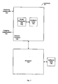
- FIG. 7 is a block diagram of an example networking system configured to support a cache entry replacement technique according to embodiments of the present invention.
- a network node 700 is depicted as including a processor 710 and a network processor 720.
- network node 700 can be a router or other piece of network equipment capable of employing embodiments of the present invention.
- network processor 720 can be a fully-custom integrated circuit (IC), a gate array or other application-specific IC (ASIC), a programmed field-programmable gate array (FPGA), discrete components or any other form of hardware.
- processor 710 has access to a software table 730, which can contain, for example, destination addresses for incoming packets.
- Software table 730 may be stored in a variety of ways, including in main memory, on disk storage or in some other fashion.
- network processor 720 includes a router processing unit 740, which is coupled to a hardware table 750.
- Hardware table 750 will typically hold some subset of the entries (e.g., destination addresses) held in software table 730.
- Route processing unit 740, together with hardware table 750 can be viewed as making up and containing the structures depicted in Fig. 3 that effect the operations of the present invention.
- Network processor 720 receives an incoming datastream 760 and processes that data stream (using route processing unit 740 and hardware table 750) to generate an outgoing datastream 770.
- hardware table 750 acts as something of a cache for the information stored in software table 730, and so would be expected to benefit from the methods and apparati described herein.
- a PRL cache entry replacement strategy provides a low-cost, hardware-based solution that is particularly well suited for software tables with large numbers of entries.
- the present invention can, in a networking environment, be extended to tables with any other kind of information that may be required to process packets.
- the present invention can be used with source information tables (e. g., those tables used for detecting fake packets being sent by hackers).
Landscapes
- Engineering & Computer Science (AREA)
- Theoretical Computer Science (AREA)
- Physics & Mathematics (AREA)
- General Engineering & Computer Science (AREA)
- General Physics & Mathematics (AREA)
- Memory System Of A Hierarchy Structure (AREA)
Claims (26)
- Cache-Controller (300) mit:einer Einrichtung zum Speichern einer potenziellen Ersatzliste (320) mit einer Vielzahl von Einträgen, wobei jeder der Einträge so konfiguriert ist, dass er einen zufälligen Cache-Zeiger-Wert (325) speichert, wobei der zufällige Cache-Zeiger-Wert auf einen Cache-Eintrag in einem Cache (302) zeigt;einer Einrichtung zum Speichern einer Vielzahl gültiger Bits (330), wobei jedes der gültigen Bits einem der Einträge entspricht;einer Einrichtung zum Bereitstellen einer Vielzahl von Zählern (335), wobei jeder der Zähler einem der Einträge entspricht;einer Einrichtung zum Auswählen eines Eintrags aus der potenziellen Ersatzliste; undeiner Einrichtung zum Ersetzen, in dem Cache, des Cache-Eintrags, auf den der in dem ausgewählten Eintrag gespeicherte zufällige Cache-Zeiger-Wert zeigt.
- Cache-Controller nach Anspruch 1, wobei die Einrichtung zum Auswählen so konfiguriert ist, dass sie den am längsten nicht mehr benutzten Cache-Eintrag der Cache-Einträge auswählt, auf die von zufälligen Cache-Zeigern in der Liste gezeigt wird, in Abhängigkeit von den Zählern.
- Cache-Controller nach Anspruch 2, wobei die Einrichtung zum Auswählen so konfiguriert ist, dass sie einen gültigen Eintrag aus der potenziellen Ersatzliste gemäß den mit den Einträgen assoziierten gültigen Bits auswählt, wobei der Cache-Controller so konfiguriert ist, dass er den Eintrag ungültig macht.
- Cache-Controller nach einem der Ansprüche 1 bis 3, der eine Einrichtung (340) zum periodischen Aktualisieren jedes Zählers aufweist.
- Cache-Controller nach Anspruch 1, der des Weiteren aufweist:einen Komparator (370), wobei
der Komparator an die Einträge gekoppelt ist, und
der Komparator so konfiguriert ist, dass er einen Cache-Zeiger-Wert (306) empfängt. - Cache-Controller nach Anspruch 5, wobei
der Komparator so konfiguriert ist, dass er den Cache-Zeiger-Wert mit einem zufälligen Cache-Zeiger-Wert vergleicht, der in wenigstens einem der Einträge gespeichert ist, und
der Komparator so konfiguriert ist, dass er wenigstens einen der Einträge ungültig macht, wenn der Cache-Zeiger-Wert mit dem zufälligen Cache-Zeiger-Wert übereinstimmt, der in dem wenigstens einen der Einträge gespeichert ist. - Cache-Controller nach Anspruch 6, wobei
der Komparator so konfiguriert ist, dass er den wenigstens einen der Einträge aufgrund dessen ungültig macht, dass er so konfiguriert ist, dass er wenigstens eines der gültigen Bits entsprechend dem wenigstens einen der Einträge löscht. - Cache-Controller nach Anspruch 5, der des Weiteren aufweist:einen Zufallszahlengenerator (360), der so konfiguriert ist, dass er einen zufälligen Cache-Zeiger-Wert erzeugt; undeine Zustandsmaschine (350), die an den Zufallszahlengenerator und die potenzielle Ersatzliste gekoppelt ist,wobei die Zustandsmaschine so konfiguriert ist, dass sie einen Cache-Zeiger-Wert ersetzt, der in einem ungültig gemachten der Einträge mit dem zufälligen Cache-Zeiger-Wert gespeichert ist.
- Cache-Controller nach Anspruch 8, wobei
die Zustandsmaschine so konfiguriert ist, dass sie den in dem ungültig gemachten der Einträge gespeicherten Cache-Zeiger-Wert durch den zufälligen Cache-Zeiger-Wert aufgrund dessen ersetzt, dass sie so konfiguriert ist, dass sie einen der Einträge liest, und
wenn der eine der Einträge ungültig gemacht ist, den zufälligen Cache-Zeiger-Wert in einen der Einträge lädt, einen der Zeiger löscht, die mit dem einen der Einträge assoziiert sind, und eines der gültigen Bits setzt, die mit dem einen der Einträge assoziiert sind. - Cache-Controller nach Anspruch 1, der des Weiteren aufweist:einen programmierbaren Taktteiler (340), der an die Zähler und ein Taktsignal (312) gekoppelt ist,wobei der programmierbare Taktteiler so konfiguriert ist, dass er eine Zählrate steuert, mit der die Zähler zählen.
- Cache-Controller nach Anspruch 1, wobei jeder der Zähler ein Sättigungszähler ist.
- Cache-Controller nach Anspruch 11, wobei die Zählrate eine Rate steuert, mit der die Zähler gesättigt werden.
- Cache-Controller nach Anspruch 1, der des Weiteren aufweist:einen programmierbaren Taktteiler (340), der an die Zähler und ein Taktsignal gekoppelt ist, wobei jeder der Zähler ein Sättigungszähler ist, und wobei der programmierbare Taktteiler so konfiguriert ist, dass er die Zählrate steuert, mit der die Zähler zählen; undeinen Prozessor (315), der an die potenzielle Ersatzliste und den programmierbaren Taktteiler gekoppelt ist,wobei der Prozessor so konfiguriert ist, dass er den programmierbaren Taktteiler konfiguriert, um die Sättigungsrate der Zähler zu steuern.
- Cache-Controller nach Anspruch 13, der des Weiteren aufweist:einen Komparator (370), wobei
der Komparator an die Einträge gekoppelt ist,
der Komparator so konfiguriert ist, dass er einen Cache-Zeiger-Wert empfängt und den Cache-Zeiger-Wert mit einem zufälligen Cache-Zeiger-Wert vergleicht, der in wenigstens einem der Einträge gespeichert ist, und
der Komparator so konfiguriert ist, dass er wenigstens einen der Einträge ungültig macht, wenn der Cache-Zeiger-Wert mit dem in dem wenigstens einen der Einträge gespeicherten zufälligen Cache-Zeiger-Wert übereinstimmt;einen Zufallszahlengenerator (360), der so konfiguriert ist, dass er einen zufälligen Cache-Zeiger-Wert erzeugt; undeine Zustandsmaschine (350), die an den Zufallszahlengenerator und die potenzielle Ersatzliste gekoppelt ist, wobeidie Zustandsmaschine so konfiguriert ist, dass sie einen Cache-Zeiger-Wert ersetzt, der in einem ungültig gemachten der Einträge mit dem zufälligen Cache-Zeiger-Wert gespeichert ist, undder Prozessor die Zustandsmaschine und den Zufallszahlengenerator aufweist. - Cache-Controller nach Anspruch 1 der des Weiteren aufweist:eine Einrichtung zum Erzeugen eines zufälligen Cache-Zeiger-Werts;eine Einrichtung zum Speichern des zufälligen Cache-Zeiger-Werts in einem Eintrag der potenziellen Ersatzliste;eine Einrichtung zum Anzeigen, dass der Eintrag gültig ist; undeine Einrichtung zum Neustarten eines Zählers, der mit dem Eintrag assoziiert ist.
- Vorrichtung nach Anspruch 15, die des Weiteren aufweist:eine Einrichtung zum Überprüfen einer Vielzahl der Zähler, um einen assoziierten der Einträge zu identifizieren, der den am längsten nicht mehr benutzten Cache-Zeiger-Wert enthält.
- Verfahren zum Ersetzen eines Cache-Eintrags in einem Cache (302), das umfasst:Speichern einer potenziellen Ersatzliste (320) mit einer Vielzahl von Einträgen, wobei jeder der Einträge so konfiguriert ist, dass er einen zufälligen Cache-Zeiger-Wert (325) speichert, wobei der zufällige Cache-Zeiger-Wert auf einen Cache-Eintrag in einem Cache (302) zeigt;Speichern einer Vielzahl gültiger Bits (330), wobei jedes der gültigen Bits einem der Einträge entspricht;Bereitstellen einer Vielzahl von Zählern (335), wobei jeder der Zähler einem der Einträge entspricht;Auswählen eines Eintrags aus der potenziellen Ersatzliste; undErsetzen, in dem Cache, des Cache-Eintrags, auf den der in dem ausgewählten Eintrag gespeicherte zufällige Cache-Zeiger-Wert zeigt.
- Verfahren nach Anspruch 17, das des Weiteren umfasst:Erzeugen eines zufälligen Cache-Zeiger-Werts;Speichern des zufälligen Cache-Zeiger-Werts in einem Eintrag (325) der potenziellen Ersatzliste (320);Anzeigen, dass der Eintrag gültig ist; undNeustarten des Zählers (335), der mit dem Eintrag assoziiert ist.
- Verfahren nach Anspruch 18, das des Weiteren umfasst:Vergleichen eines Cache-Zeiger-Werts (306) mit dem zufälligen Cache-Zeiger-Wert; undwenn der Cache-Zeiger-Wert mit dem zufälligen Cache-Zeiger-Wert übereinstimmt, Ungültigmachen des Eintrags.
- Verfahren nach Anspruch 19, das des Weiteren umfasst:Ungültigmachen des Eintrags durch Löschen des gültigen Bits (330), das mit dem Eintrag assoziiert ist.
- Verfahren nach Anspruch 19, das des Weiteren umfasst:wenn der Eintrag ungültig gemacht ist,
Erzeugen eines zufälligen Cache-Zeiger-Werts,
Speichern des zufälligen Cache-Zeiger-Werts in dem Eintrag, Anzeigen, dass der Eintrag gültig ist, und
Neustarten des Zählers. - Verfahren nach Anspruch 17, das des Weiteren umfasst:Überprüfen einer Vielzahl der Zähler, um einen assoziierten der Einträge zu identifizieren, der den am längsten nicht mehr benutzten Cache-Zeiger-Wert enthält.
- Verfahren nach Anspruch 22, wobei das Überprüfen durchgeführt wird, wenn in den Cache zu schreiben ist.
- Verfahren nach Anspruch 22, das des Weiteren umfasst:Ungültigmachen des assoziierten der Einträge durch Löschen des gültigen Bits, das mit dem assoziierten der Einträge assoziiert ist.
- Verfahren nach Anspruch 22, das des Weiteren umfasst:Erzeugen eines anderen zufälligen Cache-Zeiger-Werts;Speichern des anderen zufälligen Cache-Zeiger-Werts in dem assoziierten der Einträge;Anzeigen, dass der assoziierte der Einträge gültig ist, durch Setzen eines der gültigen Bits, die mit dem assoziierten der Einträge assoziiert sind; undNeustarten eines Zählers, der mit dem assoziierten der Einträge assoziiert ist.
- Verfahren nach Anspruch 17, das des Weiteren umfasst:Überprüfen jedes der gültigen Bits; undwenn jedes der gültigen Bits angibt, dass ein assoziierte der Einträge ungültig ist, Erzeugen eines anderen zufälligen Cache-Zeiger-Werts;Speichern des anderen zufälligen Cache-Zeiger-Werts in dem assoziierten der Einträge;Setzen jedes der gültigen Bits so, dass sie angeben, dass der assoziierte der Einträge gültig ist; undNeustarten eines Zählers, der mit dem assoziierten der Einträge assoziiert ist.
Applications Claiming Priority (3)
| Application Number | Priority Date | Filing Date | Title |
|---|---|---|---|
| US210138 | 2002-07-31 | ||
| US10/210,138 US6996678B1 (en) | 2002-07-31 | 2002-07-31 | Method and apparatus for randomized cache entry replacement |
| PCT/US2003/023943 WO2004012084A1 (en) | 2002-07-31 | 2003-07-31 | Method and apparatus for randomized cache entry replacement |
Publications (2)
| Publication Number | Publication Date |
|---|---|
| EP1525531A1 EP1525531A1 (de) | 2005-04-27 |
| EP1525531B1 true EP1525531B1 (de) | 2012-03-21 |
Family
ID=31187219
Family Applications (1)
| Application Number | Title | Priority Date | Filing Date |
|---|---|---|---|
| EP03772141A Expired - Lifetime EP1525531B1 (de) | 2002-07-31 | 2003-07-31 | Verfahren und gerät zum ersetzen eines cache-eintrags auf zufallsbasis |
Country Status (7)
| Country | Link |
|---|---|
| US (1) | US6996678B1 (de) |
| EP (1) | EP1525531B1 (de) |
| CN (1) | CN1333347C (de) |
| AT (1) | ATE550717T1 (de) |
| AU (1) | AU2003257073A1 (de) |
| CA (1) | CA2494046A1 (de) |
| WO (1) | WO2004012084A1 (de) |
Families Citing this family (21)
| Publication number | Priority date | Publication date | Assignee | Title |
|---|---|---|---|---|
| EP1667028A4 (de) * | 2003-09-19 | 2008-10-29 | Matsushita Electric Industrial Co Ltd | Cache-speicher und cache-speicher-steuerverfahren |
| US8283723B2 (en) * | 2005-02-11 | 2012-10-09 | Alpha & Omega Semiconductor Limited | MOS device with low injection diode |
| JP2007280303A (ja) * | 2006-04-11 | 2007-10-25 | Brother Ind Ltd | 情報通信システム、コンテンツカタログ情報配信方法、及びノード装置等 |
| JP4862463B2 (ja) * | 2006-04-11 | 2012-01-25 | ブラザー工業株式会社 | 情報通信システム、コンテンツカタログ情報検索方法、及びノード装置等 |
| JP4655986B2 (ja) * | 2006-04-12 | 2011-03-23 | ブラザー工業株式会社 | ノード装置、記憶制御プログラム及び情報記憶方法 |
| US8195886B2 (en) * | 2007-03-16 | 2012-06-05 | Arm Limited | Data processing apparatus and method for implementing a replacement scheme for entries of a storage unit |
| US8250302B2 (en) * | 2008-01-31 | 2012-08-21 | Hewlett-Packard Development Company, L.P. | Cache management using sampled values assigned to a request |
| CN101989236B (zh) * | 2010-11-04 | 2012-05-09 | 浙江大学 | 一种指令缓存锁实现方法 |
| DE102010054446A1 (de) | 2010-12-14 | 2012-06-14 | Giesecke & Devrient Gmbh | Portabler Datenträger mit Fehlbedienungszähler |
| US9389965B1 (en) | 2012-03-12 | 2016-07-12 | Emc Corporation | System and method for improving performance of backup storage system with future access prediction |
| US9485174B2 (en) | 2012-07-30 | 2016-11-01 | Cisco Technology, Inc. | Routing using cached source routes from message headers |
| US8868841B2 (en) * | 2012-09-04 | 2014-10-21 | Facebook, Inc. | Statistical cache promotion |
| US9170955B2 (en) * | 2012-11-27 | 2015-10-27 | Intel Corporation | Providing extended cache replacement state information |
| US9158702B2 (en) | 2012-12-28 | 2015-10-13 | Intel Corporation | Apparatus and method for implementing a scratchpad memory using priority hint |
| US9160650B2 (en) * | 2013-06-17 | 2015-10-13 | Futurewei Technologies, Inc. | Enhanced flow entry table cache replacement in a software-defined networking switch |
| US9350613B2 (en) * | 2014-01-17 | 2016-05-24 | International Business Machines Corporation | Smart dumping of network switch forwarding database |
| US10218617B2 (en) * | 2014-07-15 | 2019-02-26 | Nec Corporation | Method and network device for handling packets in a network by means of forwarding tables |
| US11237965B2 (en) * | 2014-12-31 | 2022-02-01 | Arteris, Inc. | Configurable snoop filters for cache coherent systems |
| US9507598B1 (en) * | 2015-12-15 | 2016-11-29 | International Business Machines Corporation | Auxiliary branch prediction with usefulness tracking |
| US10509732B2 (en) * | 2016-04-27 | 2019-12-17 | Advanced Micro Devices, Inc. | Selecting cache aging policy for prefetches based on cache test regions |
| CN106095552B (zh) * | 2016-06-07 | 2019-06-28 | 华中科技大学 | 一种基于i/o去重的多任务图处理方法及系统 |
Family Cites Families (10)
| Publication number | Priority date | Publication date | Assignee | Title |
|---|---|---|---|---|
| EP0452991A3 (en) * | 1985-05-29 | 1992-04-15 | Kabushiki Kaisha Toshiba | Cache system adopting an lru system |
| US5809528A (en) * | 1996-12-24 | 1998-09-15 | International Business Machines Corporation | Method and circuit for a least recently used replacement mechanism and invalidated address handling in a fully associative many-way cache memory |
| US6161167A (en) | 1997-06-27 | 2000-12-12 | Advanced Micro Devices, Inc. | Fully associate cache employing LRU groups for cache replacement and mechanism for selecting an LRU group |
| US6385699B1 (en) | 1998-04-10 | 2002-05-07 | International Business Machines Corporation | Managing an object store based on object replacement penalties and reference probabilities |
| US6490654B2 (en) * | 1998-07-31 | 2002-12-03 | Hewlett-Packard Company | Method and apparatus for replacing cache lines in a cache memory |
| US6519684B1 (en) * | 1999-11-23 | 2003-02-11 | Motorola, Inc. | Low overhead method for selecting and updating an entry in a cache memory |
| EP1182567B1 (de) * | 2000-08-21 | 2012-03-07 | Texas Instruments France | Softwaregesteuerte Cache-Speicherkonfiguration |
| US6983388B2 (en) * | 2000-10-25 | 2006-01-03 | Agere Systems Inc. | Method and apparatus for reducing leakage power in a cache memory by using a timer control signal that removes power to associated cache lines |
| US6571317B2 (en) * | 2001-05-01 | 2003-05-27 | Broadcom Corporation | Replacement data error detector |
| US6725337B1 (en) * | 2001-05-16 | 2004-04-20 | Advanced Micro Devices, Inc. | Method and system for speculatively invalidating lines in a cache |
-
2002
- 2002-07-31 US US10/210,138 patent/US6996678B1/en not_active Expired - Lifetime
-
2003
- 2003-07-31 CN CNB038182920A patent/CN1333347C/zh not_active Expired - Lifetime
- 2003-07-31 EP EP03772141A patent/EP1525531B1/de not_active Expired - Lifetime
- 2003-07-31 WO PCT/US2003/023943 patent/WO2004012084A1/en not_active Ceased
- 2003-07-31 AT AT03772141T patent/ATE550717T1/de active
- 2003-07-31 CA CA002494046A patent/CA2494046A1/en not_active Abandoned
- 2003-07-31 AU AU2003257073A patent/AU2003257073A1/en not_active Abandoned
Also Published As
| Publication number | Publication date |
|---|---|
| CA2494046A1 (en) | 2004-02-05 |
| US6996678B1 (en) | 2006-02-07 |
| AU2003257073A1 (en) | 2004-02-16 |
| CN1333347C (zh) | 2007-08-22 |
| WO2004012084A1 (en) | 2004-02-05 |
| ATE550717T1 (de) | 2012-04-15 |
| CN1672136A (zh) | 2005-09-21 |
| EP1525531A1 (de) | 2005-04-27 |
Similar Documents
| Publication | Publication Date | Title |
|---|---|---|
| EP1525531B1 (de) | Verfahren und gerät zum ersetzen eines cache-eintrags auf zufallsbasis | |
| US7437510B2 (en) | Instruction-assisted cache management for efficient use of cache and memory | |
| US7502887B2 (en) | N-way set associative cache memory and control method thereof | |
| US10789175B2 (en) | Caching policy in a multicore system on a chip (SOC) | |
| EP1551141B1 (de) | Vorrichtung und Verfahren zur effizienten Implementierung einer IP Zuordnung mit Hilfe von Prüfsummen in einer Schaltung | |
| US7284096B2 (en) | Systems and methods for data caching | |
| US7539032B2 (en) | Regular expression searching of packet contents using dedicated search circuits | |
| US7512738B2 (en) | Allocating call stack frame entries at different memory levels to functions in a program | |
| AU2010322819B2 (en) | Processing network traffic | |
| US8250306B2 (en) | Method for improving frequency-based caching algorithms by maintaining a stable history of evicted items | |
| US8412722B2 (en) | Upload manager for use in a pattern matching accelerator | |
| US7000061B2 (en) | Caching queue status updates | |
| EP1548998A1 (de) | Bitkettenpr fverfahren und einrichtung | |
| US20100070714A1 (en) | Network On Chip With Caching Restrictions For Pages Of Computer Memory | |
| US20080071779A1 (en) | Method and apparatus for managing multiple data flows in a content search system | |
| CN107528783B (zh) | 利用对前缀长度进行两个搜索阶段的ip路由缓存 | |
| US8423533B2 (en) | Multiple rule bank access scheme for use in a pattern matching accelerator | |
| US7467256B2 (en) | Processor having content addressable memory for block-based queue structures | |
| CN118259887B (zh) | 基于预测执行的带状态可编程数据平面系统及芯片 | |
| US7277990B2 (en) | Method and apparatus providing efficient queue descriptor memory access | |
| US10700975B2 (en) | Systems and methods for optimized route caching | |
| EP1980945A1 (de) | Speicherzugriffssteuervorrichtung und speicherzugriffssteuerverfahren | |
| US20050246501A1 (en) | Selective caching systems and methods | |
| EP4290821A1 (de) | Effiziente hash-tabellensuche | |
| Rooney et al. | Associative ternary cache for IP routing |
Legal Events
| Date | Code | Title | Description |
|---|---|---|---|
| PUAI | Public reference made under article 153(3) epc to a published international application that has entered the european phase |
Free format text: ORIGINAL CODE: 0009012 |
|
| 17P | Request for examination filed |
Effective date: 20050201 |
|
| AK | Designated contracting states |
Kind code of ref document: A1 Designated state(s): AT BE BG CH CY CZ DE DK EE ES FI FR GB GR HU IE IT LI LU MC NL PT RO SE SI SK TR |
|
| AX | Request for extension of the european patent |
Extension state: AL LT LV MK |
|
| DAX | Request for extension of the european patent (deleted) | ||
| RIN1 | Information on inventor provided before grant (corrected) |
Inventor name: SHARMA, RAJAN |
|
| 17Q | First examination report despatched |
Effective date: 20090707 |
|
| GRAP | Despatch of communication of intention to grant a patent |
Free format text: ORIGINAL CODE: EPIDOSNIGR1 |
|
| GRAS | Grant fee paid |
Free format text: ORIGINAL CODE: EPIDOSNIGR3 |
|
| GRAA | (expected) grant |
Free format text: ORIGINAL CODE: 0009210 |
|
| AK | Designated contracting states |
Kind code of ref document: B1 Designated state(s): AT BE BG CH CY CZ DE DK EE ES FI FR GB GR HU IE IT LI LU MC NL PT RO SE SI SK TR |
|
| REG | Reference to a national code |
Ref country code: GB Ref legal event code: FG4D |
|
| REG | Reference to a national code |
Ref country code: CH Ref legal event code: EP |
|
| REG | Reference to a national code |
Ref country code: IE Ref legal event code: FG4D |
|
| REG | Reference to a national code |
Ref country code: AT Ref legal event code: REF Ref document number: 550717 Country of ref document: AT Kind code of ref document: T Effective date: 20120415 |
|
| REG | Reference to a national code |
Ref country code: DE Ref legal event code: R096 Ref document number: 60340363 Country of ref document: DE Effective date: 20120510 |
|
| REG | Reference to a national code |
Ref country code: NL Ref legal event code: VDEP Effective date: 20120321 |
|
| PG25 | Lapsed in a contracting state [announced via postgrant information from national office to epo] |
Ref country code: FI Free format text: LAPSE BECAUSE OF FAILURE TO SUBMIT A TRANSLATION OF THE DESCRIPTION OR TO PAY THE FEE WITHIN THE PRESCRIBED TIME-LIMIT Effective date: 20120321 Ref country code: GR Free format text: LAPSE BECAUSE OF FAILURE TO SUBMIT A TRANSLATION OF THE DESCRIPTION OR TO PAY THE FEE WITHIN THE PRESCRIBED TIME-LIMIT Effective date: 20120622 |
|
| REG | Reference to a national code |
Ref country code: AT Ref legal event code: MK05 Ref document number: 550717 Country of ref document: AT Kind code of ref document: T Effective date: 20120321 |
|
| PG25 | Lapsed in a contracting state [announced via postgrant information from national office to epo] |
Ref country code: CY Free format text: LAPSE BECAUSE OF FAILURE TO SUBMIT A TRANSLATION OF THE DESCRIPTION OR TO PAY THE FEE WITHIN THE PRESCRIBED TIME-LIMIT Effective date: 20120321 |
|
| PG25 | Lapsed in a contracting state [announced via postgrant information from national office to epo] |
Ref country code: EE Free format text: LAPSE BECAUSE OF FAILURE TO SUBMIT A TRANSLATION OF THE DESCRIPTION OR TO PAY THE FEE WITHIN THE PRESCRIBED TIME-LIMIT Effective date: 20120321 Ref country code: CZ Free format text: LAPSE BECAUSE OF FAILURE TO SUBMIT A TRANSLATION OF THE DESCRIPTION OR TO PAY THE FEE WITHIN THE PRESCRIBED TIME-LIMIT Effective date: 20120321 Ref country code: SI Free format text: LAPSE BECAUSE OF FAILURE TO SUBMIT A TRANSLATION OF THE DESCRIPTION OR TO PAY THE FEE WITHIN THE PRESCRIBED TIME-LIMIT Effective date: 20120321 Ref country code: SE Free format text: LAPSE BECAUSE OF FAILURE TO SUBMIT A TRANSLATION OF THE DESCRIPTION OR TO PAY THE FEE WITHIN THE PRESCRIBED TIME-LIMIT Effective date: 20120321 Ref country code: RO Free format text: LAPSE BECAUSE OF FAILURE TO SUBMIT A TRANSLATION OF THE DESCRIPTION OR TO PAY THE FEE WITHIN THE PRESCRIBED TIME-LIMIT Effective date: 20120321 Ref country code: BE Free format text: LAPSE BECAUSE OF FAILURE TO SUBMIT A TRANSLATION OF THE DESCRIPTION OR TO PAY THE FEE WITHIN THE PRESCRIBED TIME-LIMIT Effective date: 20120321 |
|
| PG25 | Lapsed in a contracting state [announced via postgrant information from national office to epo] |
Ref country code: PT Free format text: LAPSE BECAUSE OF FAILURE TO SUBMIT A TRANSLATION OF THE DESCRIPTION OR TO PAY THE FEE WITHIN THE PRESCRIBED TIME-LIMIT Effective date: 20120723 Ref country code: SK Free format text: LAPSE BECAUSE OF FAILURE TO SUBMIT A TRANSLATION OF THE DESCRIPTION OR TO PAY THE FEE WITHIN THE PRESCRIBED TIME-LIMIT Effective date: 20120321 |
|
| PLBE | No opposition filed within time limit |
Free format text: ORIGINAL CODE: 0009261 |
|
| STAA | Information on the status of an ep patent application or granted ep patent |
Free format text: STATUS: NO OPPOSITION FILED WITHIN TIME LIMIT |
|
| PG25 | Lapsed in a contracting state [announced via postgrant information from national office to epo] |
Ref country code: NL Free format text: LAPSE BECAUSE OF FAILURE TO SUBMIT A TRANSLATION OF THE DESCRIPTION OR TO PAY THE FEE WITHIN THE PRESCRIBED TIME-LIMIT Effective date: 20120321 Ref country code: DK Free format text: LAPSE BECAUSE OF FAILURE TO SUBMIT A TRANSLATION OF THE DESCRIPTION OR TO PAY THE FEE WITHIN THE PRESCRIBED TIME-LIMIT Effective date: 20120321 Ref country code: AT Free format text: LAPSE BECAUSE OF FAILURE TO SUBMIT A TRANSLATION OF THE DESCRIPTION OR TO PAY THE FEE WITHIN THE PRESCRIBED TIME-LIMIT Effective date: 20120321 |
|
| 26N | No opposition filed |
Effective date: 20130102 |
|
| PG25 | Lapsed in a contracting state [announced via postgrant information from national office to epo] |
Ref country code: MC Free format text: LAPSE BECAUSE OF NON-PAYMENT OF DUE FEES Effective date: 20120731 Ref country code: IT Free format text: LAPSE BECAUSE OF FAILURE TO SUBMIT A TRANSLATION OF THE DESCRIPTION OR TO PAY THE FEE WITHIN THE PRESCRIBED TIME-LIMIT Effective date: 20120321 |
|
| REG | Reference to a national code |
Ref country code: CH Ref legal event code: PL |
|
| REG | Reference to a national code |
Ref country code: DE Ref legal event code: R097 Ref document number: 60340363 Country of ref document: DE Effective date: 20130102 |
|
| PG25 | Lapsed in a contracting state [announced via postgrant information from national office to epo] |
Ref country code: CH Free format text: LAPSE BECAUSE OF NON-PAYMENT OF DUE FEES Effective date: 20120731 Ref country code: LI Free format text: LAPSE BECAUSE OF NON-PAYMENT OF DUE FEES Effective date: 20120731 Ref country code: ES Free format text: LAPSE BECAUSE OF FAILURE TO SUBMIT A TRANSLATION OF THE DESCRIPTION OR TO PAY THE FEE WITHIN THE PRESCRIBED TIME-LIMIT Effective date: 20120702 |
|
| REG | Reference to a national code |
Ref country code: IE Ref legal event code: MM4A |
|
| PG25 | Lapsed in a contracting state [announced via postgrant information from national office to epo] |
Ref country code: IE Free format text: LAPSE BECAUSE OF NON-PAYMENT OF DUE FEES Effective date: 20120731 Ref country code: BG Free format text: LAPSE BECAUSE OF FAILURE TO SUBMIT A TRANSLATION OF THE DESCRIPTION OR TO PAY THE FEE WITHIN THE PRESCRIBED TIME-LIMIT Effective date: 20120621 |
|
| PG25 | Lapsed in a contracting state [announced via postgrant information from national office to epo] |
Ref country code: TR Free format text: LAPSE BECAUSE OF FAILURE TO SUBMIT A TRANSLATION OF THE DESCRIPTION OR TO PAY THE FEE WITHIN THE PRESCRIBED TIME-LIMIT Effective date: 20120321 |
|
| PG25 | Lapsed in a contracting state [announced via postgrant information from national office to epo] |
Ref country code: LU Free format text: LAPSE BECAUSE OF NON-PAYMENT OF DUE FEES Effective date: 20120731 |
|
| PG25 | Lapsed in a contracting state [announced via postgrant information from national office to epo] |
Ref country code: HU Free format text: LAPSE BECAUSE OF FAILURE TO SUBMIT A TRANSLATION OF THE DESCRIPTION OR TO PAY THE FEE WITHIN THE PRESCRIBED TIME-LIMIT Effective date: 20030731 |
|
| REG | Reference to a national code |
Ref country code: FR Ref legal event code: PLFP Year of fee payment: 13 |
|
| REG | Reference to a national code |
Ref country code: FR Ref legal event code: PLFP Year of fee payment: 14 |
|
| REG | Reference to a national code |
Ref country code: FR Ref legal event code: PLFP Year of fee payment: 15 |
|
| REG | Reference to a national code |
Ref country code: FR Ref legal event code: PLFP Year of fee payment: 16 |
|
| PGFP | Annual fee paid to national office [announced via postgrant information from national office to epo] |
Ref country code: GB Payment date: 20200727 Year of fee payment: 18 Ref country code: FR Payment date: 20200727 Year of fee payment: 18 Ref country code: DE Payment date: 20200729 Year of fee payment: 18 |
|
| REG | Reference to a national code |
Ref country code: DE Ref legal event code: R119 Ref document number: 60340363 Country of ref document: DE |
|
| GBPC | Gb: european patent ceased through non-payment of renewal fee |
Effective date: 20210731 |
|
| PG25 | Lapsed in a contracting state [announced via postgrant information from national office to epo] |
Ref country code: GB Free format text: LAPSE BECAUSE OF NON-PAYMENT OF DUE FEES Effective date: 20210731 Ref country code: DE Free format text: LAPSE BECAUSE OF NON-PAYMENT OF DUE FEES Effective date: 20220201 |
|
| PG25 | Lapsed in a contracting state [announced via postgrant information from national office to epo] |
Ref country code: FR Free format text: LAPSE BECAUSE OF NON-PAYMENT OF DUE FEES Effective date: 20210731 |
|
| P01 | Opt-out of the competence of the unified patent court (upc) registered |
Effective date: 20230525 |