EP1524699B1 - Method for forming CMOS semiconductor devices having a notched gate insulator and devices thus obtained - Google Patents
Method for forming CMOS semiconductor devices having a notched gate insulator and devices thus obtained Download PDFInfo
- Publication number
- EP1524699B1 EP1524699B1 EP03447260A EP03447260A EP1524699B1 EP 1524699 B1 EP1524699 B1 EP 1524699B1 EP 03447260 A EP03447260 A EP 03447260A EP 03447260 A EP03447260 A EP 03447260A EP 1524699 B1 EP1524699 B1 EP 1524699B1
- Authority
- EP
- European Patent Office
- Prior art keywords
- insulating layer
- gate
- source
- gate electrode
- overlap
- Prior art date
- Legal status (The legal status is an assumption and is not a legal conclusion. Google has not performed a legal analysis and makes no representation as to the accuracy of the status listed.)
- Expired - Lifetime
Links
Images
Classifications
-
- H—ELECTRICITY
- H10—SEMICONDUCTOR DEVICES; ELECTRIC SOLID-STATE DEVICES NOT OTHERWISE PROVIDED FOR
- H10D—INORGANIC ELECTRIC SEMICONDUCTOR DEVICES
- H10D64/00—Electrodes of devices having potential barriers
- H10D64/60—Electrodes characterised by their materials
- H10D64/66—Electrodes having a conductor capacitively coupled to a semiconductor by an insulator, e.g. MIS electrodes
- H10D64/671—Electrodes having a conductor capacitively coupled to a semiconductor by an insulator, e.g. MIS electrodes the conductor having lateral variation in doping or structure
-
- H—ELECTRICITY
- H10—SEMICONDUCTOR DEVICES; ELECTRIC SOLID-STATE DEVICES NOT OTHERWISE PROVIDED FOR
- H10D—INORGANIC ELECTRIC SEMICONDUCTOR DEVICES
- H10D64/00—Electrodes of devices having potential barriers
- H10D64/20—Electrodes characterised by their shapes, relative sizes or dispositions
- H10D64/27—Electrodes not carrying the current to be rectified, amplified, oscillated or switched, e.g. gates
- H10D64/311—Gate electrodes for field-effect devices
- H10D64/411—Gate electrodes for field-effect devices for FETs
- H10D64/511—Gate electrodes for field-effect devices for FETs for IGFETs
- H10D64/514—Gate electrodes for field-effect devices for FETs for IGFETs characterised by the insulating layers
- H10D64/516—Gate electrodes for field-effect devices for FETs for IGFETs characterised by the insulating layers the thicknesses being non-uniform
-
- H—ELECTRICITY
- H10—SEMICONDUCTOR DEVICES; ELECTRIC SOLID-STATE DEVICES NOT OTHERWISE PROVIDED FOR
- H10P—GENERIC PROCESSES OR APPARATUS FOR THE MANUFACTURE OR TREATMENT OF DEVICES COVERED BY CLASS H10
- H10P30/00—Ion implantation into wafers, substrates or parts of devices
- H10P30/20—Ion implantation into wafers, substrates or parts of devices into semiconductor materials, e.g. for doping
- H10P30/202—Ion implantation into wafers, substrates or parts of devices into semiconductor materials, e.g. for doping characterised by the semiconductor materials
- H10P30/204—Ion implantation into wafers, substrates or parts of devices into semiconductor materials, e.g. for doping characterised by the semiconductor materials into Group IV semiconductors
-
- H—ELECTRICITY
- H10—SEMICONDUCTOR DEVICES; ELECTRIC SOLID-STATE DEVICES NOT OTHERWISE PROVIDED FOR
- H10P—GENERIC PROCESSES OR APPARATUS FOR THE MANUFACTURE OR TREATMENT OF DEVICES COVERED BY CLASS H10
- H10P30/00—Ion implantation into wafers, substrates or parts of devices
- H10P30/20—Ion implantation into wafers, substrates or parts of devices into semiconductor materials, e.g. for doping
- H10P30/208—Ion implantation into wafers, substrates or parts of devices into semiconductor materials, e.g. for doping of electrically inactive species
-
- H—ELECTRICITY
- H10—SEMICONDUCTOR DEVICES; ELECTRIC SOLID-STATE DEVICES NOT OTHERWISE PROVIDED FOR
- H10P—GENERIC PROCESSES OR APPARATUS FOR THE MANUFACTURE OR TREATMENT OF DEVICES COVERED BY CLASS H10
- H10P30/00—Ion implantation into wafers, substrates or parts of devices
- H10P30/20—Ion implantation into wafers, substrates or parts of devices into semiconductor materials, e.g. for doping
- H10P30/21—Ion implantation into wafers, substrates or parts of devices into semiconductor materials, e.g. for doping of electrically active species
-
- H—ELECTRICITY
- H10—SEMICONDUCTOR DEVICES; ELECTRIC SOLID-STATE DEVICES NOT OTHERWISE PROVIDED FOR
- H10P—GENERIC PROCESSES OR APPARATUS FOR THE MANUFACTURE OR TREATMENT OF DEVICES COVERED BY CLASS H10
- H10P30/00—Ion implantation into wafers, substrates or parts of devices
- H10P30/20—Ion implantation into wafers, substrates or parts of devices into semiconductor materials, e.g. for doping
- H10P30/222—Ion implantation into wafers, substrates or parts of devices into semiconductor materials, e.g. for doping characterised by the angle between the ion beam and the crystal planes or the main crystal surface
Definitions
- the present invention relates to a method for forming a notched gate insulator semiconductor device and the device thus obtained. More particularly, the present invention relates to a method for the formation of a semiconductor device structure comprising first and second main electrode extensions, e.g. source and drain extensions, with controllable control electrode, e.g. gate electrode, overlap.
- first and second main electrode extensions e.g. source and drain extensions
- controllable control electrode e.g. gate electrode
- MOS Metal-Oxide-Semiconductor
- MIS Metal-Insulator-Semiconductor
- a method for the fabrication of a semiconductor device comprising abrupt source/drain extensions with controllable gate electrode overlap.
- the method comprises the steps of forming a gate structure on a semiconductor substrate, followed by forming an oxide layer on the gate and substrate.
- sidewall spacer regions are formed on the sides of the gate structure. Deep source/drain regions that do not overlap with the gate electrode are implanted in the semiconductor substrate.
- second spacer regions of silicon are formed on the sides of the sidewall spacer regions.
- Upper regions of the gate structure and the sidewall spacer regions are silicided in order to electrically connect them. Also portions of source/drain extension regions in the semiconductor substrate adjacent the gate structure are silicided.
- a first disadvantage of the method described in the above document is the number of extra steps required, i.e. "extending" the gate electrode by means of depositing silicon side wall spacers, etching back thereof and connecting the spacers to the body of the original gate electrode.
- Another disadvantage of the above method is that by the inevitable presence of an oxide layer between the body of the gate electrode and the silicon sidewall spacers, the overall gate electrode is in fact a discontinuous body of material with deleterious effects on the properties thereof.
- the device comprises a first gate insulating film, such as TiO 2 , which is formed on a channel region.
- a gate electrode is formed on the first gate insulating film.
- Source and drain regions are formed in a surface portion of a p-well region.
- the gate electrode is formed such that it may partially overlap the source/drain region.
- the TiO 2 film is subjected to either isotropic or anisotropic etching so that a portion of the TiO 2 film which lies on the source/drain region, may be removed, hereby forming a recess underneath the gate electrode.
- JP 11 163323 a semiconductor device comprising an insulating layer, a gate electrode and a source and drain is described. By adjusting the etching time of an etching process of the insulating layer, the overlap length between the gate electrode and the source and drain can be adjusted. Etching of the insulating layer is performed by wet chemical etching in a 0.3% HF solution.
- a disadvantage of EP 1 089 344 and JP 11 163323 is that the etching process of the insulating layer cannot be controlled very well.
- scaling down of electric and electronic devices plays a very important role in semiconductor processing.
- the present invention provides a semiconductor device structure comprising an insulating layer provided on a semiconductor substrate, a control electrode, e.g. a gate, provided on the insulating layer, and a first main electrode extension, e.g. source extension, and a second main electrode extension, e.g. drain extension, in the substrate, showing an overlap with the control electrode.
- the insulating layer comprises a recess near the first main electrode extension and near the second main electrode extension with respect to the control electrode.
- the recess has a depth of between 0.5 and 5 nm.
- An advantage of the recess near first and second main electrode extension is that the overlap between the control electrode and the first and second main electrode extensions can easily be controlled by means of changing the depth of the recess during the processing of the device.
- the depth of the recess may be less than a width of an overlap between the control electrode and the first main electrode extension and/or the second main electrode extension.
- the semiconductor device structure according to the present invention has a gate electrode with a length within the closed range of 20 nm to 100 nm.
- the semiconductor device structure of the present invention has an overlap between the insulating layer and the first and second main electrode extensions of between 10 and 20 % of the length of the control electrode.
- the overlap between the control electrode and the first and second main electrode extensions may preferably be between 10 and 20 % of the length of the control electrode.
- the insulating layer may be made of material comprising silicon oxide.
- the control electrode may be made of material comprising silicon.
- the control electrode may comprise polycristalline material, e.g. polysilicon.
- the present invention furthermore provides a method for processing a semiconductor device structure comprising providing an insulating layer and a control electrode, i.e. gate, onto a substrate, amorphizing a region to be implanted in the substrate to form first and second main electrode extensions, and amorphizing part of the insulating layer by means of accelerated ions under a first angle with respect to a direction perpendicular to the substrate, implanting a first main electrode extension, i.e. source extension, and a second main electrode extension, i.e.
- drain extension under a second angle with respect to a direction perpendicular to the substrate, etching back part of the insulating layer in order to reduce overlap between the control electrode and the first and second main electrode extensions to a reduced but non-zero overlap level, hereby forming recesses.
- the border between the amorphized part and the non-amorphized part of the control electrode insulating layer acts as an etch stop.
- Etching back may be performed by a dip in a HF solution with a concentration between 0.1 and 10%.
- the first angle, under which amorphizing of the first and second electrode extension regions and of part of the insulating layer occur, and the second angle, under which implantation of first and second main electrode extensions occur may substantially be the same or, in another embodiment, may be different, and may be between 0° and 45° with respect to a direction perpendicular to the plane of the substrate.
- the method may furthermore comprise activating the first and second main electrode extensions.
- activation of the first and second main electrode extensions may be performed by an annealing step selected from the group consisting of rapid thermal annealing, flash rapid thermal annealing, solid phase epitaxy regrowth or laser thermal annealing.
- the activation step may be performed after the step of etching back, because annealing may remove the amorphized parts of the gate insulating layer, hence removing the etch stop as well. Because of that, the control over the overlap between the control electrode and the first and second main electrode recesses may disappear.
- the method according to the invention may be used in many methods for fabricating semiconductor devices with gate electrodes.
- a method is described for manufacturing a device having a gate as control electrode and a source and a drain as first and second main electrodes.
- a gate insulating layer 2 is formed by means of any suitable deposition technique, depending on the insulating material used, such as for example thermally grown oxides, which may optionally be post treated such as for example nitrided silicon oxides.
- CVD chemical vapour deposition techniques
- the substrate 1 may be any kind of semiconductor material such as for example pure silicon, germanium, gallium arsenide or others.
- the substrate 1 may furthermore be a doped semiconductor, such as for example n-type silicon or p-type silicon, or a combination thereof.
- the gate insulating layer 2 may be any suitable type of insulator material, such as for example silicon dioxide.
- a gate electrode 3 is formed. Therefore a conductive layer which may for example be a semiconductor layer such as e.g. Si, a metal layer such as e.g. gold, aluminium or copper, or an inorganic conductive layer such as an indium tin oxide (ITO) layer may be deposited on top of the gate insulating layer 2 by means of any suitable deposition technique such as for example vapour deposition, sputter deposition or spin coating. Subsequently, the deposited layer may be etched back to the form of an electrode. Therefore a mask is applied onto that part of the conductive layer, which will later form the gate electrode 3.
- a conductive layer which may for example be a semiconductor layer such as e.g. Si, a metal layer such as e.g. gold, aluminium or copper, or an inorganic conductive layer such as an indium tin oxide (ITO) layer may be deposited on top of the gate insulating layer 2 by means of any suitable deposition technique such as for example vapour deposition,
- the mask may be made of any suitable material, such as for example a polymer, which may be deposited onto the conductive layer by means of for example spin coating. The conductive layer is then etched, removing the part of the conductive layer which is not covered by the mask. The same masking step may also be used to etch the part of the gate insulating layer 2 which is not under the formed gate electrode 3. Therefore, an etching solution, which may etch both the conductive material of the gate electrode 3 and the insulating material of the gate insulating layer 2, is preferably used.
- the gate electrode 3 is shown as being (poly)crystalline but the invention is not restricted hereto.
- a source extension 4 and a drain extension 5 are implanted.
- Modern source and drain junctions have to fulfil extreme requirements, such as for example very high activation, i.e. above the solid solubility limit, ultra shallow junctions (less than 10 nm depth) and a very high lateral abruptness of about 1-2 nm/decade.
- the gate leakage level at the overlap of the source or drain junctions and the gate electrode 3 must be at a controlled level, in order to find a balance between minimal gate leakage and enough overlap for optimal gate action on the junction.
- a too low overlap may cause a too small overlap between the electric fields of source, gate and drain, and hence a too slow gate action, or for example a too slow transistor.
- an additional step of amorphizing the region to be implanted is performed, according to the present invention, before the actual implanting of source and drain regions is performed.
- This step may also be referred to as pre-amorphization implant (PAI).
- PAI is a well controllable method which limits the depth to which implants can be made.
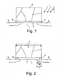
- atoms, or more precisely ions are implanted in a sufficient concentration to disrupt the originally perfect crystal lattice of the substrate 1, so that it becomes amorphous. Applying PAI will thus form regions of a shape like source extension and drain extensions 4, 5 in Fig. 1 .
- the step of amorphizing the extension volume by bombarding under a suitable first angle ensures that a part of the accelerated ions used in the bombarding will pass through the part of the gate electrode 3 nearest the semiconductor substrate 1, and will hence form an amorphized volume 6, 7 showing overlap with the gate electrode 3.
- atoms that in principle do not themselves influence the dopant concentration level such as for example Si or Ge, are implanted in the region of the extensions 4, 5.
- this may occur at energies of 8 to 20 keV, with concentrations between 5.10e14 to 3.10e15 atoms/cm 3 and under an angle of between for example 0° and 45°.
- concentrations between 5.10e14 to 3.10e15 atoms/cm 3 and under an angle of between for example 0° and 45°.
- the step of actual implanting the extension regions 4, 5 with the desired dopants may be performed.
- boron atoms may be implanted at energies of 0.5 keV with concentrations up to 1.10e15 atoms/cm 3 .
- any kind of suitable implant energy, dose or dopant type may be used in this step.
- the step of implanting may be performed under a second angle, which, in most cases, may be substantially the same as the first angle. It may thus be ensured that with the appropriate energy of the dopants, the dopants may be present in the amorphized region.
- the direction of bombarding in order to amorphize and the direction for implanting may be chosen towards the gate electrode 3 in order to achieve overlap.
- the drain extension 5 may be implanted according to a direction indicated by arrows I in Fig. 1 , including an angle a with a direction perpendicular to the substrate 1. In Fig. 1 this direction is indicated by the dashed line.
- angles and energies of the accelerated ions for amorphizing and for implanting of the dopants may be selected such that a desired overlap is realised. Selection of these quantities is interrelated and further depends on the type of semiconductor substrate 1 used.
- the semiconductor substrate 1 is amorphized.
- a part of the gate insulating layer 2 may, to a depth of for example a few nanometers, be amorphized due to the action of the amorphizing particles. In Fig. 1 this is shown as amorphous parts 6 and 7.
- This damage may be undone by annealing the semiconductor device during a further activation step, so that all of the gate insulating layer would be (poly)crystalline again.
- the damage caused in the gate insulating layer 2 by PAI may be further used during processing to achieve controllable overlap between extensions 4, 5 and the gate electrode 3 (see further).
- a structure like the one shown in Fig. 1 is the result.
- a part of the gate insulating layer 2 is removed in order to reduce the overlap between gate electrode 3 and extensions 4, 5 to a reduced but non-zero overlap level. This may be done by means of etching, e.g. by means of a wet etch.
- the material of the gate insulating layer 2, i.e. a dielectric material in general, on the one hand, and the material of the gate electrode 3 and the semiconductor substrate 1 on the other hand are different. Therefore, an etchant may be selected which selectively etches the gate insulating layer 2 but not the other materials used.
- the gate insulating layer 2 comprises amorphized parts 6, 7 and a non-amorphized or polycrystalline part. Because the etch rate of the amorphous gate insulator may differ from that of the (poly)crystalline gate insulator deeper under the gate 3, and in most cases may be higher, the border between the amorphous and polycrystalline gate insulator may be used as an etch stop. Hence, an etching solution may be required which only removes the amorphized parts 6, 7 of the gate insulating layer 2 and does not etch the polycrystalline part of the insulating layer 2.
- the etching step may be performed by dipping the semiconductor device structure in a HF solution, preferably with a concentration between 0.1 and 10 %, for example 0.2 %, during a period between for example 1 second and 5 minutes.
- a HF solution preferably with a concentration between 0.1 and 10 %, for example 0.2 %, during a period between for example 1 second and 5 minutes.
- concentration of the etching solution and etching time may depend on the depth required to etch or on the material that has to be etched. Therefore, this step of etching back the gate insulating layer 2 offers a good control over the overlap, for it is possible to select a relatively slow and therefore precise etching process.
- the gate insulating layer 2 may also be etched before the actual implant of the extensions 4, 5.
- a structure as shown in Fig. 2 may result.
- the structure differs from that in Fig. 1 only in that the amorphized parts 6 and 7 have been etched away and have become recesses 8 and 9.
- the term "recess" is intended to mean an abrupt change in the corresponding dimension, in this case in the direction between source 4 and drain 5.
- the recesses 8, 9 are mirror images of each other. However, by making use of additional masking steps and different etching conditions, it may be possible to make source and drain recesses 8, 9 with different depths.
- the recess 9 on the right hand side of the device is shown as having an etch depth e.
- the etch depth may for example be a few nanometers, preferably between 0.5 and 5 nm.
- the distance d represents the remaining overlap between drain extension 5 and gate insulating layer 2.
- the remaining overlap d between the gate insulating layer 2 and the drain extension 5 may preferably be between 10 and 20 %, for example 15 %, of the length I of the gate electrode 3.
- the latter statement only applies for gate lengths below 100 nm, preferably 50 nm or less. For larger gate lengths, a smaller overlap ratio may be selected.
- a following step may be an activation step in order to activate the implanted dopants, i.e. to build the dopants into the crystal lattice of the semiconductor substrate 1.
- This step may also be referred to as a junction anneal step.
- the junction anneal step may be performed by annealing the device with for example high ramp rates (rapid thermal anneal, or RTA), flash rapid thermal anneal (fRTA), solid phase epitaxy (SPE) or laser thermal anneal (LTA).
- RTA rapid thermal anneal
- fRTA flash rapid thermal anneal
- SPE solid phase epitaxy
- LTA laser thermal anneal
- the type of anneal and the energy concerned may be selected according to the requirements of a specific device.
- annealing may remove the "etch stop", which was formed by PAI, by curing the gate insulating layer 2. Because of that, the control over the overlap between the gate electrode 3 and the source and drain recesses 8, 9 may disappear.
- the processing of the semiconductor device structure may be finished with any desired subsequent step, depending on the kind of semiconductor device that has to be formed.
- a spacer for deep source and drain implants may be deposited in for example a low temperature plasma enhanced chemical vacuum deposition (CVD) process in the form of an oxide, at a deposition temperature of for example 400 °C. Said CVD oxide will not fill the recesses 8, 9 due to its course-grained porosity.
- CVD chemical vacuum deposition
- a balance has to be found between an overlap which is as small as possible to reduce parasitic capacitance and hot carrier effect, and an overlap which is big enough to ensure a quick response of the semiconductor device, i.e. a short switching time.
- the method of the present invention it is possible to obtain a sufficient overlap between source and drain extensions 4, 5 on the one hand, and the gate electrode 3 on the other hand.
- the total overlap between source and drain extensions 4, 5 and the gate electrode 3 is represented by t in Fig. 2 .
- the method of the present invention is particularly suitable for forming an overlapping extension 4, 5 for devices with very short gate lengths, because it gives the possibility to obtain a sufficient overlap without having to use diffusion techniques.
- Diffusion techniques suffer from less abrupt transitions between extensions 4, 5 and substrate 1 and are furthermore more difficult to control.
- it is very difficult to limit diffusion to an overlap of less than 10 nm.
- very short gate lengths of for example 50 nm down to even 30 or 20 nm, this is a too large overlap and hence the diffusion technique is then no longer useful.
- An advantage of the present invention is the simple way of tuning the overlap between the gate electrode 3 and source and drain extensions 4, 5, without the need for masks and/or spacers. This may reduce production time and hence production costs. Furthermore, the method of the present invention leads to strongly reduced gate leakage in the semiconductor device thus obtained.
Landscapes
- Insulated Gate Type Field-Effect Transistor (AREA)
- Electrodes Of Semiconductors (AREA)
- Drying Of Semiconductors (AREA)
Description
- The present invention relates to a method for forming a notched gate insulator semiconductor device and the device thus obtained. More particularly, the present invention relates to a method for the formation of a semiconductor device structure comprising first and second main electrode extensions, e.g. source and drain extensions, with controllable control electrode, e.g. gate electrode, overlap.
- The scaling of Metal-Oxide-Semiconductor (MOS) or Metal-Insulator-Semiconductor (MIS) transistor devices has reached a point where the length of the gate electrode is only a few tens of nanometers. Requirements for the source/drain extensions (the ultra-shallow junctions USJ) are mainly three-fold, i.e. very high activation (for end-of-the-roadmap devices above the solid solubility limit), ultra-shallow (towards less than 10 nm) and a very high lateral abruptness (1-2 nm/decade). The last one is also dictated by another requirement, the gate leakage level at the junction's overlap with the gate region. There is a trade-off between having no overlap for minimal gate leakage and enough overlap for optimal gate action on the junction. This trade-off is one of the major problems in scaling down the planar devices.
- In
US 6,274,446 a method is described for the fabrication of a semiconductor device comprising abrupt source/drain extensions with controllable gate electrode overlap. The method comprises the steps of forming a gate structure on a semiconductor substrate, followed by forming an oxide layer on the gate and substrate. First, sidewall spacer regions are formed on the sides of the gate structure. Deep source/drain regions that do not overlap with the gate electrode are implanted in the semiconductor substrate. In order to create overlap, second spacer regions of silicon are formed on the sides of the sidewall spacer regions. Upper regions of the gate structure and the sidewall spacer regions are silicided in order to electrically connect them. Also portions of source/drain extension regions in the semiconductor substrate adjacent the gate structure are silicided. - A first disadvantage of the method described in the above document is the number of extra steps required, i.e. "extending" the gate electrode by means of depositing silicon side wall spacers, etching back thereof and connecting the spacers to the body of the original gate electrode.
- Another disadvantage of the above method is that by the inevitable presence of an oxide layer between the body of the gate electrode and the silicon sidewall spacers, the overall gate electrode is in fact a discontinuous body of material with deleterious effects on the properties thereof.
- In
EP 1 089 344 an insulated gate field effect transistor and a method of making the same are described. The device comprises a first gate insulating film, such as TiO2, which is formed on a channel region. A gate electrode is formed on the first gate insulating film. Source and drain regions are formed in a surface portion of a p-well region. The gate electrode is formed such that it may partially overlap the source/drain region. The TiO2 film is subjected to either isotropic or anisotropic etching so that a portion of the TiO2 film which lies on the source/drain region, may be removed, hereby forming a recess underneath the gate electrode. - In
JP 11 163323 EP 1 089 344 andJP 11 163323 - It is an object of the present invention to provide a simple method of providing controlled overlap between first and second main electrode extensions, i.e. source and drain extensions, and the main electrode, i.e. gate electrode, of a semiconductor device structure.
- The above objective is accomplished by a method and device according to the present invention.
- The present invention provides a semiconductor device structure comprising an insulating layer provided on a semiconductor substrate, a control electrode, e.g. a gate, provided on the insulating layer, and a first main electrode extension, e.g. source extension, and a second main electrode extension, e.g. drain extension, in the substrate, showing an overlap with the control electrode. The insulating layer comprises a recess near the first main electrode extension and near the second main electrode extension with respect to the control electrode. The recess has a depth of between 0.5 and 5 nm. An advantage of the recess near first and second main electrode extension is that the overlap between the control electrode and the first and second main electrode extensions can easily be controlled by means of changing the depth of the recess during the processing of the device. The depth of the recess may be less than a width of an overlap between the control electrode and the first main electrode extension and/or the second main electrode extension.
- The semiconductor device structure according to the present invention has a gate electrode with a length within the closed range of 20 nm to 100 nm.
- Furthermore, the semiconductor device structure of the present invention has an overlap between the insulating layer and the first and second main electrode extensions of between 10 and 20 % of the length of the control electrode. The overlap between the control electrode and the first and second main electrode extensions may preferably be between 10 and 20 % of the length of the control electrode.
- In the device of the present invention the insulating layer may be made of material comprising silicon oxide. The control electrode may be made of material comprising silicon. The control electrode may comprise polycristalline material, e.g. polysilicon.
- The present invention furthermore provides a method for processing a semiconductor device structure comprising providing an insulating layer and a control electrode, i.e. gate, onto a substrate, amorphizing a region to be implanted in the substrate to form first and second main electrode extensions, and amorphizing part of the insulating layer by means of accelerated ions under a first angle with respect to a direction perpendicular to the substrate, implanting a first main electrode extension, i.e. source extension, and a second main electrode extension, i.e. drain extension, under a second angle with respect to a direction perpendicular to the substrate, etching back part of the insulating layer in order to reduce overlap between the control electrode and the first and second main electrode extensions to a reduced but non-zero overlap level, hereby forming recesses. The border between the amorphized part and the non-amorphized part of the control electrode insulating layer acts as an etch stop. Hence, by changing the magnitude of the part of the insulating layer that is amorphized, the depth of the recesses may be changed. Etching back may be performed by a dip in a HF solution with a concentration between 0.1 and 10%.
- In the method of the present invention the first angle, under which amorphizing of the first and second electrode extension regions and of part of the insulating layer occur, and the second angle, under which implantation of first and second main electrode extensions occur, may substantially be the same or, in another embodiment, may be different, and may be between 0° and 45° with respect to a direction perpendicular to the plane of the substrate.
- The method may furthermore comprise activating the first and second main electrode extensions. In an embodiment of the present invention, activation of the first and second main electrode extensions may be performed by an annealing step selected from the group consisting of rapid thermal annealing, flash rapid thermal annealing, solid phase epitaxy regrowth or laser thermal annealing. The activation step may be performed after the step of etching back, because annealing may remove the amorphized parts of the gate insulating layer, hence removing the etch stop as well. Because of that, the control over the overlap between the control electrode and the first and second main electrode recesses may disappear.
- These and other characteristics, features and advantages of the present invention will become apparent from the following detailed description, taken in conjunction with the accompanying drawings, which illustrate, by way of example, the principles of the invention. This description is given for the sake of example only, without limiting the scope of the invention. The reference figures quoted below refer to the attached drawings.
-
-
Fig. 1 is schematic cross-sectional view of a MOSFET device during an extension implant. -
Fig. 2 is a schematic cross-sectional view of the device ofFig.1 after etching the control electrode, e.g. gate, insulating layer. - In the different figures, the same reference figures refer to the same or analogous elements.
- The present invention will be described with respect to particular embodiments and with reference to certain drawings but the invention is not limited thereto but only by the claims. The drawings described are only schematic and are non-limiting. In the drawings, the size of some of the elements may be exaggerated and not drawn on scale for illustrative purposes. Where the term "comprising" is used in the present description and claims, it does not exclude other elements or steps.
- Moreover, the terms top, bottom, over, under and the like in the description and the claims are used for descriptive purposes and not necessarily for describing relative positions. It is to be understood that the terms so used are interchangeable under appropriate circumstances and that the embodiments of the invention described herein are capable of operation in other orientations than described or illustrated herein.
- The method according to the invention may be used in many methods for fabricating semiconductor devices with gate electrodes. In the description hereinafter, a method is described for manufacturing a device having a gate as control electrode and a source and a drain as first and second main electrodes.
- The method may comprise the following steps. On top of a semiconductor substrate 1, a
gate insulating layer 2 is formed by means of any suitable deposition technique, depending on the insulating material used, such as for example thermally grown oxides, which may optionally be post treated such as for example nitrided silicon oxides. As another example, chemical vapour deposition techniques (CVD) may be used to form high-k dielectrics such as HfO2. The substrate 1 may be any kind of semiconductor material such as for example pure silicon, germanium, gallium arsenide or others. The substrate 1 may furthermore be a doped semiconductor, such as for example n-type silicon or p-type silicon, or a combination thereof. Thegate insulating layer 2 may be any suitable type of insulator material, such as for example silicon dioxide. - In a next step a
gate electrode 3 is formed. Therefore a conductive layer which may for example be a semiconductor layer such as e.g. Si, a metal layer such as e.g. gold, aluminium or copper, or an inorganic conductive layer such as an indium tin oxide (ITO) layer may be deposited on top of thegate insulating layer 2 by means of any suitable deposition technique such as for example vapour deposition, sputter deposition or spin coating. Subsequently, the deposited layer may be etched back to the form of an electrode. Therefore a mask is applied onto that part of the conductive layer, which will later form thegate electrode 3. The mask may be made of any suitable material, such as for example a polymer, which may be deposited onto the conductive layer by means of for example spin coating. The conductive layer is then etched, removing the part of the conductive layer which is not covered by the mask. The same masking step may also be used to etch the part of thegate insulating layer 2 which is not under the formedgate electrode 3. Therefore, an etching solution, which may etch both the conductive material of thegate electrode 3 and the insulating material of thegate insulating layer 2, is preferably used. InFig. 1 , thegate electrode 3 is shown as being (poly)crystalline but the invention is not restricted hereto. - Next, a
source extension 4 and adrain extension 5 are implanted. Modern source and drain junctions have to fulfil extreme requirements, such as for example very high activation, i.e. above the solid solubility limit, ultra shallow junctions (less than 10 nm depth) and a very high lateral abruptness of about 1-2 nm/decade. Moreover, the gate leakage level at the overlap of the source or drain junctions and thegate electrode 3 must be at a controlled level, in order to find a balance between minimal gate leakage and enough overlap for optimal gate action on the junction. Although it may be advantageous, in some instances, to have zero overlap and hence minimal gate leakage, a too low overlap may cause a too small overlap between the electric fields of source, gate and drain, and hence a too slow gate action, or for example a too slow transistor. - In order to fulfil the above mentioned requirements, an additional step of amorphizing the region to be implanted is performed, according to the present invention, before the actual implanting of source and drain regions is performed. This step may also be referred to as pre-amorphization implant (PAI). PAI is a well controllable method which limits the depth to which implants can be made. Thereto, atoms, or more precisely ions, are implanted in a sufficient concentration to disrupt the originally perfect crystal lattice of the substrate 1, so that it becomes amorphous. Applying PAI will thus form regions of a shape like source extension and
drain extensions Fig. 1 . The step of amorphizing the extension volume by bombarding under a suitable first angle ensures that a part of the accelerated ions used in the bombarding will pass through the part of thegate electrode 3 nearest the semiconductor substrate 1, and will hence form anamorphized volume gate electrode 3. In a PAI, atoms that in principle do not themselves influence the dopant concentration level, such as for example Si or Ge, are implanted in the region of theextensions - After PAI, the step of actual implanting the
extension regions - The direction of bombarding in order to amorphize and the direction for implanting may be chosen towards the
gate electrode 3 in order to achieve overlap. This means that in principle two different directions are required for treatment of the source side and the drain side of the device. However, this does not entail additional masking steps, because the implants for source and drain differ anyhow, and the amorphizing step before the implanting step does not need any additional masking step. For example, thedrain extension 5 may be implanted according to a direction indicated by arrows I inFig. 1 , including an angle a with a direction perpendicular to the substrate 1. InFig. 1 this direction is indicated by the dashed line. - The angles and energies of the accelerated ions for amorphizing and for implanting of the dopants may be selected such that a desired overlap is realised. Selection of these quantities is interrelated and further depends on the type of semiconductor substrate 1 used.
- During the PAI step, not only the semiconductor substrate 1 is amorphized. Also a part of the
gate insulating layer 2 may, to a depth of for example a few nanometers, be amorphized due to the action of the amorphizing particles. InFig. 1 this is shown asamorphous parts gate insulating layer 2 by PAI may be further used during processing to achieve controllable overlap betweenextensions - After having performed the above steps, a structure like the one shown in
Fig. 1 is the result. In a next step, a part of thegate insulating layer 2 is removed in order to reduce the overlap betweengate electrode 3 andextensions gate insulating layer 2, i.e. a dielectric material in general, on the one hand, and the material of thegate electrode 3 and the semiconductor substrate 1 on the other hand are different. Therefore, an etchant may be selected which selectively etches thegate insulating layer 2 but not the other materials used. Furthermore, in one embodiment, thegate insulating layer 2 comprisesamorphized parts gate 3, and in most cases may be higher, the border between the amorphous and polycrystalline gate insulator may be used as an etch stop. Hence, an etching solution may be required which only removes theamorphized parts gate insulating layer 2 and does not etch the polycrystalline part of the insulatinglayer 2. - For example, the etching step may be performed by dipping the semiconductor device structure in a HF solution, preferably with a concentration between 0.1 and 10 %, for example 0.2 %, during a period between for example 1 second and 5 minutes. The type of etchant, concentration of the etching solution and etching time may depend on the depth required to etch or on the material that has to be etched. Therefore, this step of etching back the
gate insulating layer 2 offers a good control over the overlap, for it is possible to select a relatively slow and therefore precise etching process. Alternatively, thegate insulating layer 2 may also be etched before the actual implant of theextensions - After performing the etching step, a structure as shown in
Fig. 2 may result. The structure differs from that inFig. 1 only in that theamorphized parts recesses source 4 anddrain 5. In principle therecesses drain recesses - In
Fig. 2 , therecess 9 on the right hand side of the device is shown as having an etch depth e. The etch depth may for example be a few nanometers, preferably between 0.5 and 5 nm. The distance d represents the remaining overlap betweendrain extension 5 andgate insulating layer 2. The remaining overlap d between thegate insulating layer 2 and thedrain extension 5 may preferably be between 10 and 20 %, for example 15 %, of the length I of thegate electrode 3. The latter statement only applies for gate lengths below 100 nm, preferably 50 nm or less. For larger gate lengths, a smaller overlap ratio may be selected. - A following step may be an activation step in order to activate the implanted dopants, i.e. to build the dopants into the crystal lattice of the semiconductor substrate 1. This step may also be referred to as a junction anneal step. The junction anneal step may be performed by annealing the device with for example high ramp rates (rapid thermal anneal, or RTA), flash rapid thermal anneal (fRTA), solid phase epitaxy (SPE) or laser thermal anneal (LTA). The type of anneal and the energy concerned may be selected according to the requirements of a specific device. In the present invention, it is preferred to perform this annealing step after etching the gate insulating layer thus forming the
recesses gate insulating layer 2. Because of that, the control over the overlap between thegate electrode 3 and the source anddrain recesses - After thus forming a junction with controlled overlap and activating it, the processing of the semiconductor device structure may be finished with any desired subsequent step, depending on the kind of semiconductor device that has to be formed. For example, in a CMOS process, a spacer for deep source and drain implants may be deposited in for example a low temperature plasma enhanced chemical vacuum deposition (CVD) process in the form of an oxide, at a deposition temperature of for example 400 °C. Said CVD oxide will not fill the
recesses - In general, a balance has to be found between an overlap which is as small as possible to reduce parasitic capacitance and hot carrier effect, and an overlap which is big enough to ensure a quick response of the semiconductor device, i.e. a short switching time. With the method of the present invention it is possible to obtain a sufficient overlap between source and
drain extensions gate electrode 3 on the other hand. The total overlap between source anddrain extensions gate electrode 3 is represented by t inFig. 2 . With short gate lengths of less than 100 nm it may be sufficient when theextensions gate electrode 3 for e.g. 15% of the length of thegate electrode 3. Therefore, the method of the present invention is particularly suitable for forming an overlappingextension extensions - An advantage of the present invention is the simple way of tuning the overlap between the
gate electrode 3 and source anddrain extensions - It is to be understood that although preferred embodiments, specific constructions and configurations, as well as materials, have been discussed herein for devices according to the present invention, various changes or modifications in form and detail may be made without departing from the scope of this invention.
Claims (12)
- A CMOS semiconductor device structure comprising:- a gate insulating layer (2), deposited onto a semiconductor substrate (1);- a gate electrode (3) with a length (I) within the closed range of 20 nm to 100 nm, deposited on top of the gate insulating layer (2),- a source extension (4) and a drain extension (5) in the semiconductor substrate (1), showing an overlap with said gate electrode (3),
said insulating layer (2) comprising a recess (8,9) near the source extension (4) and near the drain extension (5) with respect to the gate electrode (3),- a spacer, said spacer being a Chemical Vapor Deposition (CVD) oxide and not filling said recesses (8,9),
wherein said recess has a depth between 0.5 and 5 nm, such that a remaining overlap (d) between the gate insulating layer (2) and the drain extension (5) is between 10 and 20% of the gate length (I). - A semiconductor device structure according to claim 1, wherein the depth (e) of the recess is less than a width (t) of an overlap between the gate electrode and the source extension (4) and/or the drain extension (5).
- A semiconductor device structure according to claim 1 or 2, wherein the gate electrode (3) has a length of 50 nm or less.
- A semiconductor device structure according to any of the previous claims, wherein the gate insulating layer (2) comprises silicon oxide.
- A semiconductor device structure according to any of the previous claims, wherein the gate electrode comprises silicon.
- A semiconductor device structure according to any of the previous claims, wherein the gate electrode comprises polycrystalline material.
- A method of processing a CMOS semiconductor device structure, the method comprising:- providing a gate insulating layer (2) onto a substrate (1);- providing a gate electrode with a length (I) within the closed range of 20nm to 100 nm , said length being defined by a mask;- amorphizing a region of the substrate (1) to be implanted to form a source and a drain extension (4,5), and amorphizing part of said insulating layer (2) by means of accelerated ions under a first angle with respect to a direction perpendicular to the substrate (1);- implanting the source and drain extension (4,5) under a second angle with respect to a direction perpendicular to the substrate (1);- etching back said insulating layer (2) in order to reduce capacitive overlap between the gate electrode (3) and source and drain extensions (4,5) to a reduced but non-zero overlap level, hereby forming recesses (8,9);- depositing a spacer for deep source and drain implants, in a low temperature plasma enhanced chemical vapour deposition (CVD) process to form a CVD oxide, which spacer does not fill the recesses (8,9), wherein amorphizing part of said insulating layer (2) defines an etch stop in said insulating layer (2) on a border between the amorphized part and a non-amorphized part, which etch stop determines the size of said recesses (8) to be formed in the insulating layer (2) to a depth between 0.5 and 5 nm, such that a remaining overlap (d) between the gate insulating layer (2) and the drain extension (5) is between 10 and 20% of the gate length (I).
- The method according to Claim 7, the method further comprising activating said source and drain extensions (4,5) after etching back the insulating layer (2).
- The method according to Claim 8, wherein activating said source and drain extensions (4,5) is performed by an annealing step selected from the group consisting of rapid thermal annealing, flash rapid thermal annealing, solid phase epitaxy regrowth or laser thermal annealing.
- The method according to any of the claims 7 to 9, wherein said first and second angle are substantially the same.
- The method according to any of the claims 7 to 10, wherein said first and second angle are between 0° and 45° with respect to a direction perpendicular to the substrate (1).
- The method according to any of the claims 7 to 11, wherein etching back said insulating layer (2) is performed by dipping in a HF solution with a concentration between 0.1 % and 10%.
Priority Applications (7)
| Application Number | Priority Date | Filing Date | Title |
|---|---|---|---|
| EP03447260A EP1524699B1 (en) | 2003-10-17 | 2003-10-17 | Method for forming CMOS semiconductor devices having a notched gate insulator and devices thus obtained |
| TW093130105A TWI360166B (en) | 2003-10-17 | 2004-10-05 | Method for forming a notched gate insulator for ad |
| US10/966,152 US7157356B2 (en) | 2003-10-17 | 2004-10-15 | Method for forming a notched gate insulator for advanced MIS semiconductor devices and devices thus obtained |
| CNB200410085542XA CN100517747C (en) | 2003-10-17 | 2004-10-15 | Method for forming notched gate insulator for advanced MIS semiconductor devices and devices obtained thereby |
| JP2004303096A JP4668579B2 (en) | 2003-10-17 | 2004-10-18 | Method for forming a semiconductor device structure |
| US11/636,817 US20070155118A1 (en) | 2003-10-17 | 2006-12-11 | Method for forming a notched gate insulator for advanced MIS semiconductor devices and devices thus obtained |
| US13/167,648 US20110309457A1 (en) | 2003-10-17 | 2011-06-23 | Method for Forming a Notched Gate Insulator for Advanced MIS Semiconductor Devices and Devices Thus Obtained |
Applications Claiming Priority (1)
| Application Number | Priority Date | Filing Date | Title |
|---|---|---|---|
| EP03447260A EP1524699B1 (en) | 2003-10-17 | 2003-10-17 | Method for forming CMOS semiconductor devices having a notched gate insulator and devices thus obtained |
Publications (2)
| Publication Number | Publication Date |
|---|---|
| EP1524699A1 EP1524699A1 (en) | 2005-04-20 |
| EP1524699B1 true EP1524699B1 (en) | 2012-12-26 |
Family
ID=34354657
Family Applications (1)
| Application Number | Title | Priority Date | Filing Date |
|---|---|---|---|
| EP03447260A Expired - Lifetime EP1524699B1 (en) | 2003-10-17 | 2003-10-17 | Method for forming CMOS semiconductor devices having a notched gate insulator and devices thus obtained |
Country Status (5)
| Country | Link |
|---|---|
| US (3) | US7157356B2 (en) |
| EP (1) | EP1524699B1 (en) |
| JP (1) | JP4668579B2 (en) |
| CN (1) | CN100517747C (en) |
| TW (1) | TWI360166B (en) |
Families Citing this family (9)
| Publication number | Priority date | Publication date | Assignee | Title |
|---|---|---|---|---|
| JP4954508B2 (en) | 2005-08-05 | 2012-06-20 | パナソニック株式会社 | Semiconductor device |
| US7595248B2 (en) | 2005-12-01 | 2009-09-29 | Intel Corporation | Angled implantation for removal of thin film layers |
| US7279758B1 (en) | 2006-05-24 | 2007-10-09 | International Business Machines Corporation | N-channel MOSFETs comprising dual stressors, and methods for forming the same |
| US20080233702A1 (en) * | 2007-03-22 | 2008-09-25 | Texas Instruments Inc. | Method of forming a recess in a semiconductor structure |
| DE102007030056B3 (en) * | 2007-06-29 | 2009-01-22 | Advanced Micro Devices, Inc., Sunnyvale | A method for blocking a pre-amorphization of a gate electrode of a transistor |
| US7795104B2 (en) * | 2008-02-13 | 2010-09-14 | Chartered Semiconductor Manufacturing Ltd. | Method for fabricating device structures having a variation in electrical conductivity |
| TWI497713B (en) * | 2011-09-14 | 2015-08-21 | 華亞科技股份有限公司 | Insulator manufacturing method |
| US9224604B2 (en) | 2012-04-05 | 2015-12-29 | Globalfoundries Inc. | Device and method for forming sharp extension region with controllable junction depth and lateral overlap |
| JP6585354B2 (en) * | 2014-03-07 | 2019-10-02 | 株式会社半導体エネルギー研究所 | Semiconductor device |
Family Cites Families (20)
| Publication number | Priority date | Publication date | Assignee | Title |
|---|---|---|---|---|
| IT1191566B (en) * | 1986-06-27 | 1988-03-23 | Sgs Microelettronica Spa | NON-LABELED SEMICONDUCTOR-TYPE MEMORY DEVICE WITH DOOR NOT CONNECTED (FLOATING GATE) ELECTRICALLY ALTERABLE WITH REDUCED TUNNEL AREA AND MANUFACTURING PROCEDURE |
| JPH0239429A (en) * | 1988-07-28 | 1990-02-08 | Matsushita Electron Corp | Manufacture of semiconductor device |
| US5223445A (en) * | 1990-05-30 | 1993-06-29 | Matsushita Electric Industrial Co., Ltd. | Large angle ion implantation method |
| JPH06283483A (en) * | 1993-03-24 | 1994-10-07 | Sanyo Electric Co Ltd | Etching method |
| US5434093A (en) * | 1994-08-10 | 1995-07-18 | Intel Corporation | Inverted spacer transistor |
| US5516707A (en) * | 1995-06-12 | 1996-05-14 | Vlsi Technology, Inc. | Large-tilted-angle nitrogen implant into dielectric regions overlaying source/drain regions of a transistor |
| US5554544A (en) * | 1995-08-09 | 1996-09-10 | United Microelectronics Corporation | Field edge manufacture of a T-gate LDD pocket device |
| JPH113990A (en) * | 1996-04-22 | 1999-01-06 | Sony Corp | Semiconductor device and manufacturing method thereof |
| JPH1140538A (en) * | 1997-07-15 | 1999-02-12 | Sony Corp | Method for manufacturing semiconductor device |
| JPH11163323A (en) * | 1997-11-26 | 1999-06-18 | Toshiba Corp | Semiconductor device and method of manufacturing this semiconductor device |
| US6127251A (en) * | 1998-09-08 | 2000-10-03 | Advanced Micro Devices, Inc. | Semiconductor device with a reduced width gate dielectric and method of making same |
| US6492695B2 (en) * | 1999-02-16 | 2002-12-10 | Koninklijke Philips Electronics N.V. | Semiconductor arrangement with transistor gate insulator |
| JP3450758B2 (en) * | 1999-09-29 | 2003-09-29 | 株式会社東芝 | Method for manufacturing field effect transistor |
| US6255165B1 (en) * | 1999-10-18 | 2001-07-03 | Advanced Micro Devices, Inc. | Nitride plug to reduce gate edge lifting |
| US6284630B1 (en) * | 1999-10-20 | 2001-09-04 | Advanced Micro Devices, Inc. | Method for fabrication of abrupt drain and source extensions for a field effect transistor |
| JP2001291861A (en) * | 2000-04-05 | 2001-10-19 | Nec Corp | MOS transistor, transistor manufacturing method |
| JP3904936B2 (en) * | 2001-03-02 | 2007-04-11 | 富士通株式会社 | Manufacturing method of semiconductor device |
| US6509612B2 (en) * | 2001-05-04 | 2003-01-21 | International Business Machines Corporation | High dielectric constant materials as gate dielectrics (insulators) |
| JP4150548B2 (en) * | 2002-08-08 | 2008-09-17 | 富士通株式会社 | Manufacturing method of semiconductor device |
| US6855989B1 (en) * | 2003-10-01 | 2005-02-15 | Advanced Micro Devices, Inc. | Damascene finfet gate with selective metal interdiffusion |
-
2003
- 2003-10-17 EP EP03447260A patent/EP1524699B1/en not_active Expired - Lifetime
-
2004
- 2004-10-05 TW TW093130105A patent/TWI360166B/en not_active IP Right Cessation
- 2004-10-15 US US10/966,152 patent/US7157356B2/en not_active Expired - Lifetime
- 2004-10-15 CN CNB200410085542XA patent/CN100517747C/en not_active Expired - Lifetime
- 2004-10-18 JP JP2004303096A patent/JP4668579B2/en not_active Expired - Lifetime
-
2006
- 2006-12-11 US US11/636,817 patent/US20070155118A1/en not_active Abandoned
-
2011
- 2011-06-23 US US13/167,648 patent/US20110309457A1/en not_active Abandoned
Also Published As
| Publication number | Publication date |
|---|---|
| US20050127436A1 (en) | 2005-06-16 |
| TW200520069A (en) | 2005-06-16 |
| US20070155118A1 (en) | 2007-07-05 |
| TWI360166B (en) | 2012-03-11 |
| CN100517747C (en) | 2009-07-22 |
| US20110309457A1 (en) | 2011-12-22 |
| JP2005123632A (en) | 2005-05-12 |
| EP1524699A1 (en) | 2005-04-20 |
| JP4668579B2 (en) | 2011-04-13 |
| US7157356B2 (en) | 2007-01-02 |
| CN1610129A (en) | 2005-04-27 |
Similar Documents
| Publication | Publication Date | Title |
|---|---|---|
| US20070267660A1 (en) | Method and apparatus for forming a semiconductor substrate with a layer structure of activated dopants | |
| US5766969A (en) | Multiple spacer formation/removal technique for forming a graded junction | |
| US7118980B2 (en) | Solid phase epitaxy recrystallization by laser annealing | |
| US20110309457A1 (en) | Method for Forming a Notched Gate Insulator for Advanced MIS Semiconductor Devices and Devices Thus Obtained | |
| US6979622B1 (en) | Semiconductor transistor having structural elements of differing materials and method of formation | |
| KR101361424B1 (en) | Semiconductor device manufacturing method | |
| JP2007515066A (en) | Semiconductor substrate with reduced junction leakage using solid phase epitaxial regrowth and method for producing the same | |
| US7009258B2 (en) | Method of building a CMOS structure on thin SOI with source/drain electrodes formed by in situ doped selective amorphous silicon | |
| US6475885B1 (en) | Source/drain formation with sub-amorphizing implantation | |
| US20060014350A1 (en) | Method for fabricating a semiconductor transistor device having ultra-shallow source/drain extensions | |
| EP1790002B1 (en) | Method of manufacturing a semiconductor device | |
| WO2004051728A1 (en) | Drain/source extension structure of a field effect transistor including doped high-k sidewall spacers | |
| US9087772B2 (en) | Device and method for forming sharp extension region with controllable junction depth and lateral overlap | |
| KR100485176B1 (en) | Fabrication method of MOS transistor | |
| US7329910B2 (en) | Semiconductor substrates and field effect transistor constructions | |
| CN100456426C (en) | Semiconductor substrate with reduced doping profile depth regrown by solid phase epitaxy and method of making same | |
| WO2004042809A1 (en) | Method of forming a nickel silicide region in a doped silicon-containing semiconductor area |
Legal Events
| Date | Code | Title | Description |
|---|---|---|---|
| PUAI | Public reference made under article 153(3) epc to a published international application that has entered the european phase |
Free format text: ORIGINAL CODE: 0009012 |
|
| AK | Designated contracting states |
Kind code of ref document: A1 Designated state(s): AT BE BG CH CY CZ DE DK EE ES FI FR GB GR HU IE IT LI LU MC NL PT RO SE SI SK TR |
|
| AX | Request for extension of the european patent |
Extension state: AL LT LV MK |
|
| 17P | Request for examination filed |
Effective date: 20050923 |
|
| AKX | Designation fees paid |
Designated state(s): AT BE BG CH CY CZ DE DK EE ES FI FR GB GR HU IE IT LI LU MC NL PT RO SE SI SK TR |
|
| RAP1 | Party data changed (applicant data changed or rights of an application transferred) |
Owner name: NXP B.V. Owner name: INTERUNIVERSITAIR MICROELEKTRONICA CENTRUM VZW |
|
| RAP1 | Party data changed (applicant data changed or rights of an application transferred) |
Owner name: IMEC Owner name: NXP B.V. |
|
| 17Q | First examination report despatched |
Effective date: 20091109 |
|
| GRAP | Despatch of communication of intention to grant a patent |
Free format text: ORIGINAL CODE: EPIDOSNIGR1 |
|
| GRAS | Grant fee paid |
Free format text: ORIGINAL CODE: EPIDOSNIGR3 |
|
| GRAA | (expected) grant |
Free format text: ORIGINAL CODE: 0009210 |
|
| AK | Designated contracting states |
Kind code of ref document: B1 Designated state(s): AT BE BG CH CY CZ DE DK EE ES FI FR GB GR HU IE IT LI LU MC NL PT RO SE SI SK TR |
|
| REG | Reference to a national code |
Ref country code: GB Ref legal event code: FG4D |
|
| REG | Reference to a national code |
Ref country code: CH Ref legal event code: EP |
|
| REG | Reference to a national code |
Ref country code: AT Ref legal event code: REF Ref document number: 590861 Country of ref document: AT Kind code of ref document: T Effective date: 20130115 |
|
| REG | Reference to a national code |
Ref country code: DE Ref legal event code: R096 Ref document number: 60342935 Country of ref document: DE Effective date: 20130307 |
|
| PG25 | Lapsed in a contracting state [announced via postgrant information from national office to epo] |
Ref country code: FI Free format text: LAPSE BECAUSE OF FAILURE TO SUBMIT A TRANSLATION OF THE DESCRIPTION OR TO PAY THE FEE WITHIN THE PRESCRIBED TIME-LIMIT Effective date: 20121226 Ref country code: SE Free format text: LAPSE BECAUSE OF FAILURE TO SUBMIT A TRANSLATION OF THE DESCRIPTION OR TO PAY THE FEE WITHIN THE PRESCRIBED TIME-LIMIT Effective date: 20121226 |
|
| REG | Reference to a national code |
Ref country code: AT Ref legal event code: MK05 Ref document number: 590861 Country of ref document: AT Kind code of ref document: T Effective date: 20121226 |
|
| REG | Reference to a national code |
Ref country code: NL Ref legal event code: VDEP Effective date: 20121226 |
|
| PG25 | Lapsed in a contracting state [announced via postgrant information from national office to epo] |
Ref country code: GR Free format text: LAPSE BECAUSE OF FAILURE TO SUBMIT A TRANSLATION OF THE DESCRIPTION OR TO PAY THE FEE WITHIN THE PRESCRIBED TIME-LIMIT Effective date: 20130327 Ref country code: SI Free format text: LAPSE BECAUSE OF FAILURE TO SUBMIT A TRANSLATION OF THE DESCRIPTION OR TO PAY THE FEE WITHIN THE PRESCRIBED TIME-LIMIT Effective date: 20121226 |
|
| PG25 | Lapsed in a contracting state [announced via postgrant information from national office to epo] |
Ref country code: BG Free format text: LAPSE BECAUSE OF FAILURE TO SUBMIT A TRANSLATION OF THE DESCRIPTION OR TO PAY THE FEE WITHIN THE PRESCRIBED TIME-LIMIT Effective date: 20130326 Ref country code: BE Free format text: LAPSE BECAUSE OF FAILURE TO SUBMIT A TRANSLATION OF THE DESCRIPTION OR TO PAY THE FEE WITHIN THE PRESCRIBED TIME-LIMIT Effective date: 20121226 Ref country code: AT Free format text: LAPSE BECAUSE OF FAILURE TO SUBMIT A TRANSLATION OF THE DESCRIPTION OR TO PAY THE FEE WITHIN THE PRESCRIBED TIME-LIMIT Effective date: 20121226 Ref country code: EE Free format text: LAPSE BECAUSE OF FAILURE TO SUBMIT A TRANSLATION OF THE DESCRIPTION OR TO PAY THE FEE WITHIN THE PRESCRIBED TIME-LIMIT Effective date: 20121226 Ref country code: CY Free format text: LAPSE BECAUSE OF FAILURE TO SUBMIT A TRANSLATION OF THE DESCRIPTION OR TO PAY THE FEE WITHIN THE PRESCRIBED TIME-LIMIT Effective date: 20121226 Ref country code: CZ Free format text: LAPSE BECAUSE OF FAILURE TO SUBMIT A TRANSLATION OF THE DESCRIPTION OR TO PAY THE FEE WITHIN THE PRESCRIBED TIME-LIMIT Effective date: 20121226 Ref country code: SK Free format text: LAPSE BECAUSE OF FAILURE TO SUBMIT A TRANSLATION OF THE DESCRIPTION OR TO PAY THE FEE WITHIN THE PRESCRIBED TIME-LIMIT Effective date: 20121226 Ref country code: ES Free format text: LAPSE BECAUSE OF FAILURE TO SUBMIT A TRANSLATION OF THE DESCRIPTION OR TO PAY THE FEE WITHIN THE PRESCRIBED TIME-LIMIT Effective date: 20130406 |
|
| PG25 | Lapsed in a contracting state [announced via postgrant information from national office to epo] |
Ref country code: NL Free format text: LAPSE BECAUSE OF FAILURE TO SUBMIT A TRANSLATION OF THE DESCRIPTION OR TO PAY THE FEE WITHIN THE PRESCRIBED TIME-LIMIT Effective date: 20121226 Ref country code: RO Free format text: LAPSE BECAUSE OF FAILURE TO SUBMIT A TRANSLATION OF THE DESCRIPTION OR TO PAY THE FEE WITHIN THE PRESCRIBED TIME-LIMIT Effective date: 20121226 Ref country code: PT Free format text: LAPSE BECAUSE OF FAILURE TO SUBMIT A TRANSLATION OF THE DESCRIPTION OR TO PAY THE FEE WITHIN THE PRESCRIBED TIME-LIMIT Effective date: 20130426 |
|
| PG25 | Lapsed in a contracting state [announced via postgrant information from national office to epo] |
Ref country code: DK Free format text: LAPSE BECAUSE OF FAILURE TO SUBMIT A TRANSLATION OF THE DESCRIPTION OR TO PAY THE FEE WITHIN THE PRESCRIBED TIME-LIMIT Effective date: 20121226 |
|
| PLBE | No opposition filed within time limit |
Free format text: ORIGINAL CODE: 0009261 |
|
| STAA | Information on the status of an ep patent application or granted ep patent |
Free format text: STATUS: NO OPPOSITION FILED WITHIN TIME LIMIT |
|
| 26N | No opposition filed |
Effective date: 20130927 |
|
| PG25 | Lapsed in a contracting state [announced via postgrant information from national office to epo] |
Ref country code: IT Free format text: LAPSE BECAUSE OF FAILURE TO SUBMIT A TRANSLATION OF THE DESCRIPTION OR TO PAY THE FEE WITHIN THE PRESCRIBED TIME-LIMIT Effective date: 20121226 |
|
| REG | Reference to a national code |
Ref country code: DE Ref legal event code: R097 Ref document number: 60342935 Country of ref document: DE Effective date: 20130927 |
|
| PG25 | Lapsed in a contracting state [announced via postgrant information from national office to epo] |
Ref country code: MC Free format text: LAPSE BECAUSE OF FAILURE TO SUBMIT A TRANSLATION OF THE DESCRIPTION OR TO PAY THE FEE WITHIN THE PRESCRIBED TIME-LIMIT Effective date: 20121226 |
|
| REG | Reference to a national code |
Ref country code: CH Ref legal event code: PL |
|
| REG | Reference to a national code |
Ref country code: IE Ref legal event code: MM4A |
|
| PG25 | Lapsed in a contracting state [announced via postgrant information from national office to epo] |
Ref country code: LI Free format text: LAPSE BECAUSE OF NON-PAYMENT OF DUE FEES Effective date: 20131031 Ref country code: CH Free format text: LAPSE BECAUSE OF NON-PAYMENT OF DUE FEES Effective date: 20131031 |
|
| PG25 | Lapsed in a contracting state [announced via postgrant information from national office to epo] |
Ref country code: IE Free format text: LAPSE BECAUSE OF NON-PAYMENT OF DUE FEES Effective date: 20131017 |
|
| PG25 | Lapsed in a contracting state [announced via postgrant information from national office to epo] |
Ref country code: TR Free format text: LAPSE BECAUSE OF FAILURE TO SUBMIT A TRANSLATION OF THE DESCRIPTION OR TO PAY THE FEE WITHIN THE PRESCRIBED TIME-LIMIT Effective date: 20121226 |
|
| PG25 | Lapsed in a contracting state [announced via postgrant information from national office to epo] |
Ref country code: HU Free format text: LAPSE BECAUSE OF FAILURE TO SUBMIT A TRANSLATION OF THE DESCRIPTION OR TO PAY THE FEE WITHIN THE PRESCRIBED TIME-LIMIT; INVALID AB INITIO Effective date: 20031017 Ref country code: LU Free format text: LAPSE BECAUSE OF NON-PAYMENT OF DUE FEES Effective date: 20131017 |
|
| REG | Reference to a national code |
Ref country code: FR Ref legal event code: PLFP Year of fee payment: 14 |
|
| REG | Reference to a national code |
Ref country code: FR Ref legal event code: PLFP Year of fee payment: 15 |
|
| REG | Reference to a national code |
Ref country code: FR Ref legal event code: PLFP Year of fee payment: 16 |
|
| PGFP | Annual fee paid to national office [announced via postgrant information from national office to epo] |
Ref country code: GB Payment date: 20220922 Year of fee payment: 20 |
|
| PGFP | Annual fee paid to national office [announced via postgrant information from national office to epo] |
Ref country code: FR Payment date: 20220921 Year of fee payment: 20 |
|
| PGFP | Annual fee paid to national office [announced via postgrant information from national office to epo] |
Ref country code: DE Payment date: 20220920 Year of fee payment: 20 |
|
| P01 | Opt-out of the competence of the unified patent court (upc) registered |
Effective date: 20230513 |
|
| REG | Reference to a national code |
Ref country code: DE Ref legal event code: R071 Ref document number: 60342935 Country of ref document: DE |
|
| REG | Reference to a national code |
Ref country code: GB Ref legal event code: PE20 Expiry date: 20231016 |
|
| PG25 | Lapsed in a contracting state [announced via postgrant information from national office to epo] |
Ref country code: GB Free format text: LAPSE BECAUSE OF EXPIRATION OF PROTECTION Effective date: 20231016 |
|
| PG25 | Lapsed in a contracting state [announced via postgrant information from national office to epo] |
Ref country code: GB Free format text: LAPSE BECAUSE OF EXPIRATION OF PROTECTION Effective date: 20231016 |