EP1523230A1 - Circuit board assembly main and connector boards and connector pins for same - Google Patents
Circuit board assembly main and connector boards and connector pins for same Download PDFInfo
- Publication number
- EP1523230A1 EP1523230A1 EP04256250A EP04256250A EP1523230A1 EP 1523230 A1 EP1523230 A1 EP 1523230A1 EP 04256250 A EP04256250 A EP 04256250A EP 04256250 A EP04256250 A EP 04256250A EP 1523230 A1 EP1523230 A1 EP 1523230A1
- Authority
- EP
- European Patent Office
- Prior art keywords
- connector
- board
- circuit board
- face
- printed circuit
- Prior art date
- Legal status (The legal status is an assumption and is not a legal conclusion. Google has not performed a legal analysis and makes no representation as to the accuracy of the status listed.)
- Withdrawn
Links
- 238000004519 manufacturing process Methods 0.000 description 3
- 229910000679 solder Inorganic materials 0.000 description 3
- 238000002788 crimping Methods 0.000 description 2
- 230000000712 assembly Effects 0.000 description 1
- 238000000429 assembly Methods 0.000 description 1
- 230000009977 dual effect Effects 0.000 description 1
- 230000000694 effects Effects 0.000 description 1
- 238000003780 insertion Methods 0.000 description 1
- 230000037431 insertion Effects 0.000 description 1
- 230000013011 mating Effects 0.000 description 1
- 239000002184 metal Substances 0.000 description 1
- 238000000034 method Methods 0.000 description 1
- 229920000098 polyolefin Polymers 0.000 description 1
- 238000005476 soldering Methods 0.000 description 1
- 229920005992 thermoplastic resin Polymers 0.000 description 1
Images




Classifications
-
- H—ELECTRICITY
- H05—ELECTRIC TECHNIQUES NOT OTHERWISE PROVIDED FOR
- H05K—PRINTED CIRCUITS; CASINGS OR CONSTRUCTIONAL DETAILS OF ELECTRIC APPARATUS; MANUFACTURE OF ASSEMBLAGES OF ELECTRICAL COMPONENTS
- H05K1/00—Printed circuits
- H05K1/02—Details
- H05K1/14—Structural association of two or more printed circuits
- H05K1/141—One or more single auxiliary printed circuits mounted on a main printed circuit, e.g. modules, adapters
-
- H—ELECTRICITY
- H01—ELECTRIC ELEMENTS
- H01R—ELECTRICALLY-CONDUCTIVE CONNECTIONS; STRUCTURAL ASSOCIATIONS OF A PLURALITY OF MUTUALLY-INSULATED ELECTRICAL CONNECTING ELEMENTS; COUPLING DEVICES; CURRENT COLLECTORS
- H01R12/00—Structural associations of a plurality of mutually-insulated electrical connecting elements, specially adapted for printed circuits, e.g. printed circuit boards [PCB], flat or ribbon cables, or like generally planar structures, e.g. terminal strips, terminal blocks; Coupling devices specially adapted for printed circuits, flat or ribbon cables, or like generally planar structures; Terminals specially adapted for contact with, or insertion into, printed circuits, flat or ribbon cables, or like generally planar structures
- H01R12/50—Fixed connections
- H01R12/51—Fixed connections for rigid printed circuits or like structures
- H01R12/52—Fixed connections for rigid printed circuits or like structures connecting to other rigid printed circuits or like structures
-
- H—ELECTRICITY
- H01—ELECTRIC ELEMENTS
- H01R—ELECTRICALLY-CONDUCTIVE CONNECTIONS; STRUCTURAL ASSOCIATIONS OF A PLURALITY OF MUTUALLY-INSULATED ELECTRICAL CONNECTING ELEMENTS; COUPLING DEVICES; CURRENT COLLECTORS
- H01R12/00—Structural associations of a plurality of mutually-insulated electrical connecting elements, specially adapted for printed circuits, e.g. printed circuit boards [PCB], flat or ribbon cables, or like generally planar structures, e.g. terminal strips, terminal blocks; Coupling devices specially adapted for printed circuits, flat or ribbon cables, or like generally planar structures; Terminals specially adapted for contact with, or insertion into, printed circuits, flat or ribbon cables, or like generally planar structures
- H01R12/70—Coupling devices
- H01R12/71—Coupling devices for rigid printing circuits or like structures
- H01R12/712—Coupling devices for rigid printing circuits or like structures co-operating with the surface of the printed circuit or with a coupling device exclusively provided on the surface of the printed circuit
- H01R12/714—Coupling devices for rigid printing circuits or like structures co-operating with the surface of the printed circuit or with a coupling device exclusively provided on the surface of the printed circuit with contacts abutting directly the printed circuit; Button contacts therefore provided on the printed circuit
-
- H—ELECTRICITY
- H01—ELECTRIC ELEMENTS
- H01R—ELECTRICALLY-CONDUCTIVE CONNECTIONS; STRUCTURAL ASSOCIATIONS OF A PLURALITY OF MUTUALLY-INSULATED ELECTRICAL CONNECTING ELEMENTS; COUPLING DEVICES; CURRENT COLLECTORS
- H01R12/00—Structural associations of a plurality of mutually-insulated electrical connecting elements, specially adapted for printed circuits, e.g. printed circuit boards [PCB], flat or ribbon cables, or like generally planar structures, e.g. terminal strips, terminal blocks; Coupling devices specially adapted for printed circuits, flat or ribbon cables, or like generally planar structures; Terminals specially adapted for contact with, or insertion into, printed circuits, flat or ribbon cables, or like generally planar structures
- H01R12/70—Coupling devices
- H01R12/7005—Guiding, mounting, polarizing or locking means; Extractors
- H01R12/7011—Locking or fixing a connector to a PCB
- H01R12/707—Soldering or welding
-
- H—ELECTRICITY
- H05—ELECTRIC TECHNIQUES NOT OTHERWISE PROVIDED FOR
- H05K—PRINTED CIRCUITS; CASINGS OR CONSTRUCTIONAL DETAILS OF ELECTRIC APPARATUS; MANUFACTURE OF ASSEMBLAGES OF ELECTRICAL COMPONENTS
- H05K2201/00—Indexing scheme relating to printed circuits covered by H05K1/00
- H05K2201/04—Assemblies of printed circuits
- H05K2201/048—Second PCB mounted on first PCB by inserting in window or holes of the first PCB
-
- H—ELECTRICITY
- H05—ELECTRIC TECHNIQUES NOT OTHERWISE PROVIDED FOR
- H05K—PRINTED CIRCUITS; CASINGS OR CONSTRUCTIONAL DETAILS OF ELECTRIC APPARATUS; MANUFACTURE OF ASSEMBLAGES OF ELECTRICAL COMPONENTS
- H05K2201/00—Indexing scheme relating to printed circuits covered by H05K1/00
- H05K2201/09—Shape and layout
- H05K2201/09009—Substrate related
- H05K2201/09027—Non-rectangular flat PCB, e.g. circular
-
- H—ELECTRICITY
- H05—ELECTRIC TECHNIQUES NOT OTHERWISE PROVIDED FOR
- H05K—PRINTED CIRCUITS; CASINGS OR CONSTRUCTIONAL DETAILS OF ELECTRIC APPARATUS; MANUFACTURE OF ASSEMBLAGES OF ELECTRICAL COMPONENTS
- H05K2201/00—Indexing scheme relating to printed circuits covered by H05K1/00
- H05K2201/09—Shape and layout
- H05K2201/09145—Edge details
-
- H—ELECTRICITY
- H05—ELECTRIC TECHNIQUES NOT OTHERWISE PROVIDED FOR
- H05K—PRINTED CIRCUITS; CASINGS OR CONSTRUCTIONAL DETAILS OF ELECTRIC APPARATUS; MANUFACTURE OF ASSEMBLAGES OF ELECTRICAL COMPONENTS
- H05K2201/00—Indexing scheme relating to printed circuits covered by H05K1/00
- H05K2201/10—Details of components or other objects attached to or integrated in a printed circuit board
- H05K2201/10227—Other objects, e.g. metallic pieces
- H05K2201/10295—Metallic connector elements partly mounted in a hole of the PCB
- H05K2201/10303—Pin-in-hole mounted pins
-
- H—ELECTRICITY
- H05—ELECTRIC TECHNIQUES NOT OTHERWISE PROVIDED FOR
- H05K—PRINTED CIRCUITS; CASINGS OR CONSTRUCTIONAL DETAILS OF ELECTRIC APPARATUS; MANUFACTURE OF ASSEMBLAGES OF ELECTRICAL COMPONENTS
- H05K2201/00—Indexing scheme relating to printed circuits covered by H05K1/00
- H05K2201/10—Details of components or other objects attached to or integrated in a printed circuit board
- H05K2201/10431—Details of mounted components
- H05K2201/10439—Position of a single component
- H05K2201/10446—Mounted on an edge
-
- H—ELECTRICITY
- H05—ELECTRIC TECHNIQUES NOT OTHERWISE PROVIDED FOR
- H05K—PRINTED CIRCUITS; CASINGS OR CONSTRUCTIONAL DETAILS OF ELECTRIC APPARATUS; MANUFACTURE OF ASSEMBLAGES OF ELECTRICAL COMPONENTS
- H05K3/00—Apparatus or processes for manufacturing printed circuits
- H05K3/36—Assembling printed circuits with other printed circuits
- H05K3/366—Assembling printed circuits with other printed circuits substantially perpendicularly to each other
Definitions
- the present invention relates to circuit board assemblies, and more particularly to a first circuit board and a second connector board that are connected together.
- Electronically controlled tools such as DC tools
- the cable is typically a two-way conduit for providing motor power, signals, and other control lines between circuit boards and/or electrical components located onboard both the controller and the tool.
- one way of connecting the tool to a cable without adding length is to dress the cable directly into the tool without using a connector.
- This approach makes replacement of the cable, a high wear item, difficult.
- An alternative approach is to integrate one side of a connector at one end of the tool for connection to a mating connector of a cable.
- this approach undesirably adds significant length to the tool.
- a circuit board assembly comprising a main board having a first face and a second face and terminating in an edge having a mounting area, the mounting area comprising at least one mounting pad on at least one of the first and the second faces; a connector board having a first face and a second face and comprising at least one through hole between the first and second faces; and at least one connector pin disposed in said at least one through hole and having a portion extending beyond each of the first and second faces of the connector board; characterised in that the edge of the main board and the second face of the connector board are abutted and the portion of the connector pin extending beyond the second face of the connector board is attached to said at least one mounting pad.
- a printed circuit board having at least one electrical component, the circuit board comprising a first face and a second face and terminating in an edge having a mounting area, characterised in that the mounting area is configured for receiving a connector board and comprising at least one mounting pad on at least one of the first and the second faces.
- a connector board for connecting a plurality of connector pins to a printed circuit board, comprising a first face and a second face and a thickness having slots for receiving the main printed circuit board and at least one through hole between the first and second face configured to receive a plurality of said connector pins.
- Circuit board assembly 5 Shown in Fig. 1 is a conventional circuit board assembly 5 that is typically installed into a housing of an electronically controlled tool an has an integral moulded connector 18.
- Circuit board assembly 5 includes a main printed circuit board 10 that is orthogonally fitted into slots in a first connector board 12 and attached thereto via solder disposed between solder pads 17 located on each board.
- First connector board 12 is in turn connected to a second connector board 14 via board-to-board pins 16 which are electrically connected to connector pins 19.
- Second connector board 14 is provided to facilitate rerouting of trace connections between the connector pins 19.
- Connector pins 19 are partially embedded in moulded connector 18 and extend outward for connection to a female receptacle of a connecting cable (not shown).
- Moulded connector 18 is typically made of a thermoplastic resin that is moulded around connector pins 19, board-to-board pins 16, and the connector sockets (not shown) that join them. Generally, electrical connections are established between connector pins 19 and electrical components that are located either on main board 10 via associated printed circuitry (not shown) or elsewhere in the tool housing via connecting cable 24.
- the conventional circuit board assembly 5 described above suffers from numerous drawbacks including the addition of significant length to the tool. Moreover, a plurality of parts and manufacturing steps are required to make the conventional connector assembly thus making it both labour intensive and more costly to manufacture.
- the present circuit board assembly is easily assembled to achieve an integrated connector that reduces both the number of component parts and the associated space required to house them.
- Figs. 2 to 9 show the present circuit board assembly 20 which comprises a main board 50 and connector board 30 that are joined together, preferably in an orthogonal orientation as shown in Fig. 4.
- Main board 50 is a printed circuit board having a first face and a second face that include electronic and/or electrical components 56, such as integrated circuits, and associated circuitry.
- Connector board 30 has at least one and, preferably, a plurality of through holes 31 (shown in Fig. 9) in which are contained a corresponding at least one and, preferably, a plurality of connector pins 32.
- a corresponding at least one and, preferably, a plurality of connector pins 32 As shown in the enlarged view of Fig. 6, preferably disposed circumferentially and located along the length of each of the connector pins 32 are flanges 34 for seating against the connector board 30 to prevent further forward axial motion once inserted into the plurality of holes 31.
- connector pins 32 are hollow on one end to permit the insertion of conducting wires to be attached as described in detail below.
- each of the plurality of holes 31 of connector board 30 is plated with metal around its periphery to form bonding rings 35.
- connector pins 32 are soldered to bonding rings 35 achieving both the electrical interconnection of each pin to the bonding ring while mechanically preventing the pins from axially moving backward out of their respective holes.
- a printed circuit 33 (only part of the printed circuit being shown in Fig. 9) may be provided, as is known in the art, with traces on either or both side of connector board 30 to provide various interconnections between the pins.
- wire interconnects may be used to connect the connector pins 32.
- connector board 30 contains receiving slots 36 for receiving tab portions 55 located on both sides of a receiving notch 54 in the end of main board 50 that is to be joined.
- receiving notch 54 is configured to receive the thickness of connector board 30 so that the tab portions 55 are flush with the surface of the connector board 30 from which the connector pins 32 outwardly extend.
- main board 50 at the rear edge of main board 50 on at least one and preferably both sides thereof, is at least one mounting pad that preferably is a plurality of electrical contact pads 52 which comprise part of the printed circuit 53 (only part of the printed circuit being shown).
- the printed circuit may be contained on both sides of the main board 50 with the two halves of the circuit being interconnected by plated through-holes (not shown), as is known in the art.
- Electronic and/or electrical components are mounted on the card, as is known in the art, with only a few component 56 being shown in the drawing by way of example.
- attachment of the main board 50 to the connector board 30 is achieved by soldering at least one connector pin 32 to a corresponding contact pad 52 after the tab portions 55 of main board 50 are inserted into the receiving slots 36 of connector board 30. As shown by the connecting arrows between Figs. 8 and 9, this is accomplished by locating at least one hole 31 positioned on either or both sides of the main board 50 so that each is aligned with a corresponding contact pad 52. To achieve a secure bond between the main board an the connector board, it is preferred that a plurality of electrical contact pads 52 are provided on each side of main board 50 with a plurality of corresponding holes 31 being aligned in two rows between which receiving slots 36 are located.
- Connector board 30 is preferably a printed circuit board on which printed circuit traces and the electrical contact pads can be provided to achieve desired interconnection configurations between the connector pins 32 and connector pads 52 of main board 50. In this fashion, the connector pins that are used to mechanically secure the main board to the connector board may also serve the dual purpose of providing electrical connections between the boards.
- the connector board 30 is provided in a thickness that is sufficient to support the connector pins. Generally, thicknesses of about one-eighth of an inch (3.18mm) inadequately accomplish this purpose. As shown in Fig. 7, receiving slots 36 are advantageously shaped to allow tab portions 55 to be easily inserted with, preferably, an interference fit being provided there between.
- receiving slots 36 can be configured for a looser (e.g., larger) fit than a size-on-size fit.
- FIGs. 10 to 11 if connecting cables are to be included, the individual wires on one end are first stripped and then attached to conventional connector pins 19 by crimping the pins onto the individual wires.
- These conventional pins can include those such as connector pins available from Moles Inc. Lisle, IL, UA, to which a conventional pin connector is attached as shown in Fig. 11.
- outer cable shield 25 of connecting cable 24 is then pulled away from the other end of the cable and the individual wires are similarly stripped and then inserted through the proper holes in connector board 30 for connection to the hollow ends of connector pins 32.
- heat-shrinkable tubing 37 and 38 such as that available as NP203 polyolefin tubing from Nelco Product, Inc., Pembroke, MA, USA, is included both over the cable and the individual wires, respectively, as shown.
- Connector pins 32 are then crimped in similar fashion to connector pins 19 over the individual wire strands with the difference being that they include a circumferential flange as described above.
- a crimping tool such as a Model M22520/2-01 crimp tool available from Daniels Manufacturing Corporation, Orlando, FL, USA, is used to crimp connector pins 32.
- Connector pins 32 are then pulled through connector board 30 until connector pin flanges 34 seat against a first face of the connector board.
- the connector pins 32 are then soldered in position to bonding rings 32 on a second face of the connector board 30 after which the shrink tubing 38 is slid over the pins and then shrunk.
- the outer cable shield 25 is then slid back toward connector board 30 and the heat shrink tubing 37 is then slid and shrunk over both ends of the cable shield.
- Tab portions 55 of main board 50 are then inserted into receiving slots 36 of connector board 30 so that the end of main board 50 is preferably flush with connector board 30 as shown.
- Assembly of circuit board assembly 20 is then continued by inserting into the plurality of holes 31 additional connector pins 32 required to make the connections needed with a connector of a controller cable.
- the connector pins 32 are pulled through connector board 30 until connector pin flanges 34 seat against a first face of the connector board and then soldered in position to bonding rings 35 on a second face of the connector board 30.
- these pins are soldered directly to the contact pads to provide the mechanical connection between the connector board 30 and the main board 50.
- An electrical connection is also established by the solder 57 between the connector pins 32 and the contact pads 52 that may be used to connect the pins with other electrical components if electrical connections, such as those shown as printed circuit 53 in Fig. 8 and/or other wire interconnects, are made with contact pads 52.
- electrical connections such as those shown as printed circuit 53 in Fig. 8 and/or other wire interconnects, are made with contact pads 52.
- a printed circuit such as that shown as printed circuit 33 in Fig. 9
- wire interconnects may be used to connect the connector pins 32 thereby achieving various desired interconnections therebetween.
- the completed circuit board assembly shown in Figs. 2 to 7 produced thereby may then be inserted into a tool housing 60 such as that shown in Fig. 12, which preferably includes a shoulder 62 that captures the connector board 30 upon sliding it therein. Also preferred is the use of an O-ring groove 63 into which an O-ring is placed to help secure and seal the circuit board assembly 20 in tool housing 60.
- circuit board assembly may be incorporated into other electrical devices having pin connectors in which a robust mechanical assembly and compact design are desired.
Landscapes
- Engineering & Computer Science (AREA)
- Microelectronics & Electronic Packaging (AREA)
- Coupling Device And Connection With Printed Circuit (AREA)
Abstract
A circuit board assembly comprising a main board (50), a
connector board (30) and connector pins (52). The main
board has a first face and a second face and terminates in
an edge having a mounting area, the mounting area comprising
at least one mounting pad (52) on at least one of the faces.
The connector board has two faces and at least one through
hole (31) between the faces. A connector pin (52) is
disposed in each hole and having a portion extending beyond
each of the faces of the connector board, wherein the edge
of the main board and the second face of the connector board
are abutted and the portion of the connector pin extending
beyond the second face of the connector board is attached to
the at least one mounting pad.
Description
- The present invention relates to circuit board assemblies, and more particularly to a first circuit board and a second connector board that are connected together.
- Electronically controlled tools, such as DC tools, are typically designed to be driven from a controller using a cable between the controller and the tool to permit the tool to be moved freely inside of a workspace. The cable is typically a two-way conduit for providing motor power, signals, and other control lines between circuit boards and/or electrical components located onboard both the controller and the tool. In designing such tools, however, it is often desirable to minimise the length of the tool to facilitate fitting the tool into confined spaces. To help achieve this, one way of connecting the tool to a cable without adding length is to dress the cable directly into the tool without using a connector. However, this approach makes replacement of the cable, a high wear item, difficult. An alternative approach is to integrate one side of a connector at one end of the tool for connection to a mating connector of a cable. However, by integrating the connector, this approach undesirably adds significant length to the tool.
- According to a first aspect of the present invention, there is provided a circuit board assembly comprising a main board having a first face and a second face and terminating in an edge having a mounting area, the mounting area comprising at least one mounting pad on at least one of the first and the second faces; a connector board having a first face and a second face and comprising at least one through hole between the first and second faces; and at least one connector pin disposed in said at least one through hole and having a portion extending beyond each of the first and second faces of the connector board; characterised in that the edge of the main board and the second face of the connector board are abutted and the portion of the connector pin extending beyond the second face of the connector board is attached to said at least one mounting pad.
- According to a second aspect of the present invention, there is provided a printed circuit board having at least one electrical component, the circuit board comprising a first face and a second face and terminating in an edge having a mounting area, characterised in that the mounting area is configured for receiving a connector board and comprising at least one mounting pad on at least one of the first and the second faces.
- According to a third aspect of the present invention, there is provided a connector board for connecting a plurality of connector pins to a printed circuit board, comprising a first face and a second face and a thickness having slots for receiving the main printed circuit board and at least one through hole between the first and second face configured to receive a plurality of said connector pins.
- For a better understanding of the invention and to show how the same may be carried into effect, reference will now be made, by way of example, to the accompanying drawings, in which:-
- Fig. 1 is a perspective view of a conventional circuit board assembly according to the prior art;
- Fig. 2 is a perspective view of the present circuit board assembly;
- Fig. 3 is a top view of the circuit board assembly shown in Fig. 2;
- Fig. 4 is a side view of the circuit board assembly shown in Fig. 2;
- Fig. 5 is a bottom view of the circuit board assembly shown in Fig. 2;
- Fig. 6 is an enlarged view of the portion shown bounded by the dashed-dotted line in Fig. 4;
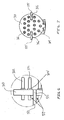
- Fig. 7 is an end view of the circuit board assembly shown in Fig. 2;
- Fig. 8 is a partial planar view of the unassembled edge of a main board for the present circuit board assembly;
- Fig. 9 is a front view of an unassembled connector board for the present circuit board assembly;
- Fig. 10 is a perspective view of a connecting cable in the process of being assembled to a connector board of the present circuit board assembly;
- Fig. 11 is a bottom view of the connecting cable and connector board of Fig. 10 being attached to a main board of the present circuit board assembly; and
- Fig. 12 is a partial sectional view of a tool housing configured to incorporate the present circuit board assembly.
-
- Shown in Fig. 1 is a conventional circuit board assembly 5 that is typically installed into a housing of an electronically controlled tool an has an integral
moulded connector 18. Circuit board assembly 5 includes a main printedcircuit board 10 that is orthogonally fitted into slots in afirst connector board 12 and attached thereto via solder disposed betweensolder pads 17 located on each board.First connector board 12 is in turn connected to asecond connector board 14 via board-to-board pins 16 which are electrically connected toconnector pins 19.Second connector board 14 is provided to facilitate rerouting of trace connections between theconnector pins 19.Connector pins 19 are partially embedded inmoulded connector 18 and extend outward for connection to a female receptacle of a connecting cable (not shown).Moulded connector 18 is typically made of a thermoplastic resin that is moulded aroundconnector pins 19, board-to-board pins 16, and the connector sockets (not shown) that join them. Generally, electrical connections are established betweenconnector pins 19 and electrical components that are located either onmain board 10 via associated printed circuitry (not shown) or elsewhere in the tool housing via connectingcable 24. - Although generally acceptable, the conventional circuit board assembly 5 described above suffers from numerous drawbacks including the addition of significant length to the tool. Moreover, a plurality of parts and manufacturing steps are required to make the conventional connector assembly thus making it both labour intensive and more costly to manufacture. The present circuit board assembly, on the other hand, is easily assembled to achieve an integrated connector that reduces both the number of component parts and the associated space required to house them.
- Figs. 2 to 9 show the present
circuit board assembly 20 which comprises amain board 50 andconnector board 30 that are joined together, preferably in an orthogonal orientation as shown in Fig. 4. -
Main board 50 is a printed circuit board having a first face and a second face that include electronic and/orelectrical components 56, such as integrated circuits, and associated circuitry.Connector board 30 has at least one and, preferably, a plurality of through holes 31 (shown in Fig. 9) in which are contained a corresponding at least one and, preferably, a plurality ofconnector pins 32. As shown in the enlarged view of Fig. 6, preferably disposed circumferentially and located along the length of each of theconnector pins 32 areflanges 34 for seating against theconnector board 30 to prevent further forward axial motion once inserted into the plurality ofholes 31. Preferably,connector pins 32 are hollow on one end to permit the insertion of conducting wires to be attached as described in detail below. - As shown in Fig. 9, each of the plurality of
holes 31 ofconnector board 30 is plated with metal around its periphery to formbonding rings 35. As discussed in detail below,connector pins 32 are soldered to bondingrings 35 achieving both the electrical interconnection of each pin to the bonding ring while mechanically preventing the pins from axially moving backward out of their respective holes. A printed circuit 33 (only part of the printed circuit being shown in Fig. 9) may be provided, as is known in the art, with traces on either or both side ofconnector board 30 to provide various interconnections between the pins.
Alternatively to or in conjunction with the printed circuit, wire interconnects (not shown) may be used to connect theconnector pins 32. Preferably,connector board 30 containsreceiving slots 36 for receivingtab portions 55 located on both sides of a receivingnotch 54 in the end ofmain board 50 that is to be joined. As seen best in Figs. 3, 6 and 8, receivingnotch 54 is configured to receive the thickness ofconnector board 30 so that thetab portions 55 are flush with the surface of theconnector board 30 from which theconnector pins 32 outwardly extend. - As shown in Fig. 8, at the rear edge of
main board 50 on at least one and preferably both sides thereof, is at least one mounting pad that preferably is a plurality ofelectrical contact pads 52 which comprise part of the printed circuit 53 (only part of the printed circuit being shown). The printed circuit may be contained on both sides of themain board 50 with the two halves of the circuit being interconnected by plated through-holes (not shown), as is known in the art. Electronic and/or electrical components are mounted on the card, as is known in the art, with only afew component 56 being shown in the drawing by way of example. - As discussed in greater detail below, attachment of the
main board 50 to theconnector board 30 is achieved by soldering at least oneconnector pin 32 to acorresponding contact pad 52 after thetab portions 55 ofmain board 50 are inserted into thereceiving slots 36 ofconnector board 30. As shown by the connecting arrows between Figs. 8 and 9, this is accomplished by locating at least onehole 31 positioned on either or both sides of themain board 50 so that each is aligned with acorresponding contact pad 52. To achieve a secure bond between the main board an the connector board, it is preferred that a plurality ofelectrical contact pads 52 are provided on each side ofmain board 50 with a plurality ofcorresponding holes 31 being aligned in two rows between which receivingslots 36 are located.
Connector board 30 is preferably a printed circuit board on which printed circuit traces and the electrical contact pads can be provided to achieve desired interconnection configurations between theconnector pins 32 andconnector pads 52 ofmain board 50. In this fashion, the connector pins that are used to mechanically secure the main board to the connector board may also serve the dual purpose of providing electrical connections between the boards. - To help angular motion of the
connector pins 32 while connecting and disconnecting a cable, it is preferred that theconnector board 30 is provided in a thickness that is sufficient to support the connector pins. Generally, thicknesses of about one-eighth of an inch (3.18mm) inadequately accomplish this purpose. As shown in Fig. 7, receivingslots 36 are advantageously shaped to allowtab portions 55 to be easily inserted with, preferably, an interference fit being provided there between. - Alternatively, receiving
slots 36 can be configured for a looser (e.g., larger) fit than a size-on-size fit. - A typical assembly of the present circuit board assembly will now be described. Turning to Figs. 10 to 11, if connecting cables are to be included, the individual wires on one end are first stripped and then attached to
conventional connector pins 19 by crimping the pins onto the individual wires. These conventional pins can include those such as connector pins available from Moles Inc. Lisle, IL, UA, to which a conventional pin connector is attached as shown in Fig. 11. As shown in Fig. 10outer cable shield 25 of connectingcable 24 is then pulled away from the other end of the cable and the individual wires are similarly stripped and then inserted through the proper holes inconnector board 30 for connection to the hollow ends ofconnector pins 32. Preferably, heat-shrinkable tubing Connector pins 32 are then crimped in similar fashion toconnector pins 19 over the individual wire strands with the difference being that they include a circumferential flange as described above. Preferably, a crimping tool such as a Model M22520/2-01 crimp tool available from Daniels Manufacturing Corporation, Orlando, FL, USA, is used to crimpconnector pins 32. Connector pins 32 are then pulled throughconnector board 30 untilconnector pin flanges 34 seat against a first face of the connector board. The connector pins 32 are then soldered in position to bonding rings 32 on a second face of theconnector board 30 after which theshrink tubing 38 is slid over the pins and then shrunk. Theouter cable shield 25 is then slid back towardconnector board 30 and the heat shrinktubing 37 is then slid and shrunk over both ends of the cable shield.Tab portions 55 ofmain board 50 are then inserted into receivingslots 36 ofconnector board 30 so that the end ofmain board 50 is preferably flush withconnector board 30 as shown. - Assembly of
circuit board assembly 20 is then continued by inserting into the plurality ofholes 31 additional connector pins 32 required to make the connections needed with a connector of a controller cable. As described above, the connector pins 32 are pulled throughconnector board 30 untilconnector pin flanges 34 seat against a first face of the connector board and then soldered in position to bonding rings 35 on a second face of theconnector board 30. In the case of connector pins 32 that are aligned with and adjacent to contactpads 52, these pins are soldered directly to the contact pads to provide the mechanical connection between theconnector board 30 and themain board 50. An electrical connection is also established by thesolder 57 between the connector pins 32 and thecontact pads 52 that may be used to connect the pins with other electrical components if electrical connections, such as those shown as printedcircuit 53 in Fig. 8 and/or other wire interconnects, are made withcontact pads 52. As described above, a printed circuit (such as that shown as printedcircuit 33 in Fig. 9) and/or wire interconnects (not shown) may be used to connect the connector pins 32 thereby achieving various desired interconnections therebetween. - The completed circuit board assembly shown in Figs. 2 to 7 produced thereby may then be inserted into a tool housing 60 such as that shown in Fig. 12, which preferably includes a
shoulder 62 that captures theconnector board 30 upon sliding it therein. Also preferred is the use of an O-ring groove 63 into which an O-ring is placed to help secure and seal thecircuit board assembly 20 in tool housing 60. - Although described above with respect to use with electric tools, it is contemplated that the present circuit board assembly may be incorporated into other electrical devices having pin connectors in which a robust mechanical assembly and compact design are desired.
- Although shown with examples of electrical components and circuitry it is to be understood that various other electrical components with different trace circuit configurations may be utilised.
Claims (16)
- A circuit board assembly (20) comprising a main board (50) having a first face and a second face and terminating in an edge having a mounting area, the mounting area comprising at least one mounting pad (52) on at least one of the first and the second faces; a connector board (30) having a first face and a second face and comprising at least one through hole (31) between the first and second faces; and at least one connector pin (32) disposed in said at least one through hole and having a portion extending beyond each of the first and second faces of the connector board; characterised in that the edge of the main board (50) and the second face of the connector board (30) are abutted and the portion of the connector pin (32) extending beyond the second face of the connector board is attached to said at least one mounting pad (52).
- An assembly according to claim 1, wherein the or each connector pin (32) further comprises a flange (34) disposed circumferentially and located along the length of the pin that seats against the first side of the connector board (30).
- An assembly according to claim 1 or 2, wherein said at least one mounting pad is a plurality of electrical contact pads (52) located on one or both sides of the mounting board.
- An assembly according to claim 3 and comprising a plurality of said connector pins (32) to include at least one row of pins aligned with and attached to a plurality of said electrical contact pads (52) on the edge of the main board (50).
- An assembly according to any one of the preceding claims, wherein the edge of the main board (50) adjacent the mounting area includes a slot with adjacent tab portions (55) to receive the second face of the connector board.
- An assembly according to claim 5, wherein the connector board (30) comprises slots (36) for receiving the tab portions (55) of the main board.
- An assembly according to claim 3 or 4 or to claim 5 or 6 as appendant to claim 3, wherein the main board (50) is a printed circuit board having traces connecting at least one of the electrical contact pads (52) to at least one electrical component located on the printed circuit board.
- An assembly according to any one of the preceding claims and comprising a plurality of said connector pins (32), wherein the connector board (30) is a printed circuit board with traces that electrically connect the connecting pins.
- A printed circuit board (50) having at least one electrical component (56), the circuit board comprising a first face and a second face and terminating in an edge having a mounting area, characterised in that the mounting area is configured for receiving a connector board and comprising at least one mounting pad (52) on at least one of the first and the second faces.
- A printed circuit board according to claim 9, wherein the edge of the main board (50) adjacent the mounting area includes a slot with adjacent tab portions (55) for receiving a connector board (30).
- A printed circuit board according to claim 9 or 10, wherein said at least one mounting pad is a plurality of electrical contact pads (52) located on one or both sides of the mounting board.
- A printed circuit board according to claim 11 and comprising traces connecting at least one of the electrical contact pads (52) to at least one electrical component (56) located on the printed circuit board (50).
- A connector board (30) for connecting a plurality of connector pins (32) to a printed circuit board (50), comprising a first face and a second face and a thickness having slots (36) for receiving the main printed circuit board and at least one through hole (31) between the first and second faces configured to receive a plurality of said connector pins.
- A connector board according to claim 13, wherein at least some of the plurality of holes (31) are aligned in two rows between which the slots (36) for receiving the main printed circuit board are located.
- A connector board according to claim 13, wherein each said hole (31) located in the connector board (30) comprises bonding rings (32) plated around their peripheries on one side of the connector board.
- A connector board according to claim 15, wherein the connector board (30) is a printed circuit board with traces that electrically connect the bonding rings (32).
Applications Claiming Priority (2)
| Application Number | Priority Date | Filing Date | Title |
|---|---|---|---|
| US681733 | 2001-05-30 | ||
| US10/681,733 US6893271B2 (en) | 2003-10-08 | 2003-10-08 | Circuit board assembly, main and connector boards, and connector pins for same |
Publications (1)
| Publication Number | Publication Date |
|---|---|
| EP1523230A1 true EP1523230A1 (en) | 2005-04-13 |
Family
ID=34314130
Family Applications (1)
| Application Number | Title | Priority Date | Filing Date |
|---|---|---|---|
| EP04256250A Withdrawn EP1523230A1 (en) | 2003-10-08 | 2004-10-08 | Circuit board assembly main and connector boards and connector pins for same |
Country Status (3)
| Country | Link |
|---|---|
| US (1) | US6893271B2 (en) |
| EP (1) | EP1523230A1 (en) |
| CA (1) | CA2484016A1 (en) |
Cited By (1)
| Publication number | Priority date | Publication date | Assignee | Title |
|---|---|---|---|---|
| WO2009071387A1 (en) * | 2007-12-03 | 2009-06-11 | Robert Bosch Gmbh | Printed circuit board comprising contact pins connected thereto |
Families Citing this family (6)
| Publication number | Priority date | Publication date | Assignee | Title |
|---|---|---|---|---|
| US7180302B2 (en) * | 2004-07-16 | 2007-02-20 | Simula, Inc | Method and system for determining cracks and broken components in armor |
| US7350288B2 (en) * | 2005-08-05 | 2008-04-01 | Infineon Technologies Ag | Card stiffener and insertion tool |
| US9454188B2 (en) * | 2014-06-03 | 2016-09-27 | Apple Inc. | Electronic device structures joined using shrinking and expanding attachment structures |
| ES2778106T3 (en) * | 2015-10-28 | 2020-08-07 | Hewlett Packard Development Co Lp | Liquid level indicator |
| US20230307854A1 (en) * | 2022-03-25 | 2023-09-28 | Dell Products L.P. | System and methods for coupling a connector to circuit board and cable |
| GB202400814D0 (en) * | 2024-01-22 | 2024-03-06 | Agco Int Gmbh | Anti-capillary connector |
Citations (9)
| Publication number | Priority date | Publication date | Assignee | Title |
|---|---|---|---|---|
| DE3138285A1 (en) * | 1981-09-25 | 1983-04-07 | Siemens AG, 1000 Berlin und 8000 München | Supporting plate which can be plugged vertically onto a printed-circuit board by means of a plurality of rows of conductive pins, and a method for producing the supporting plate |
| US4723925A (en) * | 1987-03-02 | 1988-02-09 | Woven Electronics Corporation | Crimp contact for a printed circuit board and method |
| FR2608328A1 (en) * | 1986-12-10 | 1988-06-17 | Ducellier & Cie | Method for connecting a first printed circuit to a second printed circuit, and printed circuits which enable such a method to be implemented and which are interconnected in this way |
| DE3919273A1 (en) * | 1989-06-13 | 1990-12-20 | Bosch Gmbh Robert | Circuit board system with main and orthogonal extra boards - has extra board clamps, each as integral snap-action hook with outwards protrusion |
| WO1992019024A1 (en) * | 1991-04-16 | 1992-10-29 | North American Specialities Corporation | Solder-bearing lead |
| EP0599121A1 (en) * | 1992-11-23 | 1994-06-01 | Siemens Nixdorf Informationssysteme Aktiengesellschaft | Process for producing plated through-hole printed circuit boards having very small solder lands or no solder lands |
| WO1996024175A1 (en) * | 1995-01-31 | 1996-08-08 | The Whitaker Corporation | Press-fit connecting pin and electronic device using the same |
| EP0804059A1 (en) * | 1996-04-23 | 1997-10-29 | Nec Corporation | Structure for mounting an electrical module on a board |
| EP1035759A2 (en) * | 1999-03-11 | 2000-09-13 | Lucent Technologies Inc. | Edge-mountable integrated circuit package and method of attaching the same to a printed wiring board |
Family Cites Families (13)
| Publication number | Priority date | Publication date | Assignee | Title |
|---|---|---|---|---|
| US3993936A (en) | 1975-08-29 | 1976-11-23 | Intermen Corporation | Connector arrangement for printed circuit card |
| US4109298A (en) | 1976-07-26 | 1978-08-22 | Texas Instruments Incorporated | Connector with printed wiring board structure |
| JPS57193094A (en) | 1981-05-18 | 1982-11-27 | Matsushita Electric Industrial Co Ltd | Electronic circuit part and method of mounting same |
| US4922378A (en) | 1986-08-01 | 1990-05-01 | Texas Instruments Incorporated | Baseboard for orthogonal chip mount |
| US5031072A (en) | 1986-08-01 | 1991-07-09 | Texas Instruments Incorporated | Baseboard for orthogonal chip mount |
| US4715820A (en) * | 1986-09-29 | 1987-12-29 | Amp Incorporated | Connection system for printed circuit boards |
| US4762500A (en) * | 1986-12-04 | 1988-08-09 | Amp Incorporated | Impedance matched electrical connector |
| US5317480A (en) | 1992-08-21 | 1994-05-31 | At&T Bell Laboratories | Circuit pack interconnection |
| US5484965A (en) | 1994-09-30 | 1996-01-16 | Allen-Bradley Company, Inc. | Circuit board adapted to receive a single in-line package module |
| US5644475A (en) | 1994-09-30 | 1997-07-01 | Allen-Bradley Company, Inc. | Solder mask for a finger connector on a single in-line package module |
| US5853297A (en) | 1996-06-19 | 1998-12-29 | Distributed Processing Technology Corporation | System and method for co-planar and nearly co-planar printed circuit board extension docking system |
| US5823790A (en) | 1996-07-29 | 1998-10-20 | Lucent Technologies Inc. | Connector for attaching a cable to a printed circuit board |
| US6453532B1 (en) | 1999-06-04 | 2002-09-24 | Seagate Technology Llc | Apparatus for aligning pins on a printed circuit board connector for a disc drive |
-
2003
- 2003-10-08 US US10/681,733 patent/US6893271B2/en not_active Expired - Lifetime
-
2004
- 2004-10-06 CA CA002484016A patent/CA2484016A1/en not_active Abandoned
- 2004-10-08 EP EP04256250A patent/EP1523230A1/en not_active Withdrawn
Patent Citations (9)
| Publication number | Priority date | Publication date | Assignee | Title |
|---|---|---|---|---|
| DE3138285A1 (en) * | 1981-09-25 | 1983-04-07 | Siemens AG, 1000 Berlin und 8000 München | Supporting plate which can be plugged vertically onto a printed-circuit board by means of a plurality of rows of conductive pins, and a method for producing the supporting plate |
| FR2608328A1 (en) * | 1986-12-10 | 1988-06-17 | Ducellier & Cie | Method for connecting a first printed circuit to a second printed circuit, and printed circuits which enable such a method to be implemented and which are interconnected in this way |
| US4723925A (en) * | 1987-03-02 | 1988-02-09 | Woven Electronics Corporation | Crimp contact for a printed circuit board and method |
| DE3919273A1 (en) * | 1989-06-13 | 1990-12-20 | Bosch Gmbh Robert | Circuit board system with main and orthogonal extra boards - has extra board clamps, each as integral snap-action hook with outwards protrusion |
| WO1992019024A1 (en) * | 1991-04-16 | 1992-10-29 | North American Specialities Corporation | Solder-bearing lead |
| EP0599121A1 (en) * | 1992-11-23 | 1994-06-01 | Siemens Nixdorf Informationssysteme Aktiengesellschaft | Process for producing plated through-hole printed circuit boards having very small solder lands or no solder lands |
| WO1996024175A1 (en) * | 1995-01-31 | 1996-08-08 | The Whitaker Corporation | Press-fit connecting pin and electronic device using the same |
| EP0804059A1 (en) * | 1996-04-23 | 1997-10-29 | Nec Corporation | Structure for mounting an electrical module on a board |
| EP1035759A2 (en) * | 1999-03-11 | 2000-09-13 | Lucent Technologies Inc. | Edge-mountable integrated circuit package and method of attaching the same to a printed wiring board |
Cited By (1)
| Publication number | Priority date | Publication date | Assignee | Title |
|---|---|---|---|---|
| WO2009071387A1 (en) * | 2007-12-03 | 2009-06-11 | Robert Bosch Gmbh | Printed circuit board comprising contact pins connected thereto |
Also Published As
| Publication number | Publication date |
|---|---|
| US20050079746A1 (en) | 2005-04-14 |
| CA2484016A1 (en) | 2005-04-08 |
| US6893271B2 (en) | 2005-05-17 |
Similar Documents
| Publication | Publication Date | Title |
|---|---|---|
| EP0840407B1 (en) | Electrical connector between a pair of printed circuit boards | |
| US5769645A (en) | Electrical connector for dual printed circuit boards | |
| EP3392984B1 (en) | Press-fit circuit board connector | |
| US9806443B1 (en) | Press-fit circuit board connector | |
| EP3249751A2 (en) | Press-fit circuit board connector | |
| US4723916A (en) | Pin plug and socket connector using insulation displacement contacts | |
| US20090130888A1 (en) | Cable connector | |
| US6190196B1 (en) | Cable connector assembly | |
| US6893271B2 (en) | Circuit board assembly, main and connector boards, and connector pins for same | |
| KR102031835B1 (en) | Connector for Connecting Board | |
| US5984696A (en) | Hybrid connector and right angle female member and male member thereof | |
| JP4391310B2 (en) | Multi-pole connector and assembly method thereof | |
| US7112067B1 (en) | Connector assembly for printed circuit board interconnection | |
| JPS59139582A (en) | Electrically conducting device | |
| CN210310146U (en) | Rearview mirror assembly | |
| US20070141913A1 (en) | Electrical contact assembly and method of manufacturing thereof | |
| US6027376A (en) | Connector for integrated circuit chip | |
| JP4807312B2 (en) | Multipole coaxial connector | |
| WO1994027345A1 (en) | Connector component contact system | |
| JP2005183273A (en) | Connector contact holding structure | |
| JP3313074B2 (en) | Conversion connector | |
| KR100664647B1 (en) | connector | |
| US5691251A (en) | Connector kit, and connector assembly | |
| CN109755782A (en) | connector device | |
| US7517226B2 (en) | Helical contact connector system |
Legal Events
| Date | Code | Title | Description |
|---|---|---|---|
| PUAI | Public reference made under article 153(3) epc to a published international application that has entered the european phase |
Free format text: ORIGINAL CODE: 0009012 |
|
| AK | Designated contracting states |
Kind code of ref document: A1 Designated state(s): AT BE BG CH CY CZ DE DK EE ES FI FR GB GR HU IE IT LI LU MC NL PL PT RO SE SI SK TR |
|
| AX | Request for extension of the european patent |
Extension state: AL HR LT LV MK |
|
| 17P | Request for examination filed |
Effective date: 20051012 |
|
| AKX | Designation fees paid |
Designated state(s): DE FR GB IT SE |
|
| STAA | Information on the status of an ep patent application or granted ep patent |
Free format text: STATUS: THE APPLICATION HAS BEEN WITHDRAWN |
|
| 18W | Application withdrawn |
Effective date: 20061107 |