EP1522889A2 - Method and apparatus for generating an OPC segmentation - Google Patents
Method and apparatus for generating an OPC segmentation Download PDFInfo
- Publication number
- EP1522889A2 EP1522889A2 EP04256064A EP04256064A EP1522889A2 EP 1522889 A2 EP1522889 A2 EP 1522889A2 EP 04256064 A EP04256064 A EP 04256064A EP 04256064 A EP04256064 A EP 04256064A EP 1522889 A2 EP1522889 A2 EP 1522889A2
- Authority
- EP
- European Patent Office
- Prior art keywords
- layout
- segmentation
- segment
- gradient
- model
- Prior art date
- Legal status (The legal status is an assumption and is not a legal conclusion. Google has not performed a legal analysis and makes no representation as to the accuracy of the status listed.)
- Ceased
Links
Images


Classifications
-
- G—PHYSICS
- G03—PHOTOGRAPHY; CINEMATOGRAPHY; ANALOGOUS TECHNIQUES USING WAVES OTHER THAN OPTICAL WAVES; ELECTROGRAPHY; HOLOGRAPHY
- G03F—PHOTOMECHANICAL PRODUCTION OF TEXTURED OR PATTERNED SURFACES, e.g. FOR PRINTING, FOR PROCESSING OF SEMICONDUCTOR DEVICES; MATERIALS THEREFOR; ORIGINALS THEREFOR; APPARATUS SPECIALLY ADAPTED THEREFOR
- G03F1/00—Originals for photomechanical production of textured or patterned surfaces, e.g., masks, photo-masks, reticles; Mask blanks or pellicles therefor; Containers specially adapted therefor; Preparation thereof
- G03F1/36—Masks having proximity correction features; Preparation thereof, e.g. optical proximity correction [OPC] design processes
-
- G—PHYSICS
- G03—PHOTOGRAPHY; CINEMATOGRAPHY; ANALOGOUS TECHNIQUES USING WAVES OTHER THAN OPTICAL WAVES; ELECTROGRAPHY; HOLOGRAPHY
- G03F—PHOTOMECHANICAL PRODUCTION OF TEXTURED OR PATTERNED SURFACES, e.g. FOR PRINTING, FOR PROCESSING OF SEMICONDUCTOR DEVICES; MATERIALS THEREFOR; ORIGINALS THEREFOR; APPARATUS SPECIALLY ADAPTED THEREFOR
- G03F7/00—Photomechanical, e.g. photolithographic, production of textured or patterned surfaces, e.g. printing surfaces; Materials therefor, e.g. comprising photoresists; Apparatus specially adapted therefor
- G03F7/70—Microphotolithographic exposure; Apparatus therefor
- G03F7/70425—Imaging strategies, e.g. for increasing throughput or resolution, printing product fields larger than the image field or compensating lithography- or non-lithography errors, e.g. proximity correction, mix-and-match, stitching or double patterning
- G03F7/70433—Layout for increasing efficiency or for compensating imaging errors, e.g. layout of exposure fields for reducing focus errors; Use of mask features for increasing efficiency or for compensating imaging errors
- G03F7/70441—Optical proximity correction [OPC]
Definitions
- the invention relates to the process of designing and fabricating semiconductor chips. More specifically, the invention relates to a method and an semiconductor chips. More specifically, the invention relates to a method and an apparatus for generating an optical proximity correction (OPC) segmentation.
- OPC optical proximity correction
- a layout is often subjected to a model-based optical proximity correction (OPC) operation, which adjusts the layout to compensate for optical effects.
- OPC optical proximity correction
- optical proximity correction is used in this specification, more generally the term as used herein refers to correction for any specified proximity effects, e.g. optical, micro-loading, etch, resist, etc.
- OPC optical proximity correction
- edges in the layout are divided into segments, and each segment is adjusted with a negative or a positive bias based upon a deviation between the desired layout and the simulated layout.
- dissecting a layout of an integrated circuit is facilitated based on modeled intensity gradients to produce a segmentation for an optical proximity correction (OPC) process.
- OPC optical proximity correction
- the system performs a model-based simulation on the layout to generate intensity gradients along edges of features in the layout.
- the system also generates a segmentation for edges in the layout based upon the intensity gradients, wherein the segmentation is used by a subsequent OPC process in generating corrections for the layout.
- the system generates the segmentation for edges in the layout based upon the intensity gradients along the edges, and then uses the segment lengths to dissect the edges in the layout, thereby generating the segmentation for the layout.
- the system identifies a segment length for an edge by using a predetermined association to map an intensity gradient angle (and possibly magnitude) to the segment length.
- generating the segmentation involves selecting a segmentation for a line-end in the layout from a set of predetermined line-end segmentations based upon intensity gradients associated with the line-end.
- the segmentation for the line-end is selected based upon a magnitude (and possibly angle) of an intensity gradient associated with the line-end.
- the system performs the model-based simulation by dividing each edge in the layout into minimum-sized segments, and then performing a model-based simulation to determine an intensity gradient for each minimum-sized segment.
- the system determines a gradient for a given minimum-sized segment by performing a model-based simulation at two tangential points along the segment to determine a tangential component of the gradient.
- the system determines the gradient for the given minimum-sized segment by performing a model-based simulation at two points along a normal to the segment to determine a normal component of the gradient.
- the gradient may also be determined through other methods. For example, a numerical gradient could be used that produces an instantaneous gradient rather than the average gradient. This has the advantage of only requiring one model evaluation per segment, so it is computationally cheaper.
- the system performs a subsequent dissection on problem areas in the layout after initial OPC operations take place.
- the same subsequent evaluation can be used to merge segments that do not need as much correction once correction has commenced.
- the system calibrates the association between gradients and segment lengths by first modeling an intensity gradient across a test pattern, and then identifying target regions in the test pattern that have a large amount of correction shift variation. Next, the system maps intensity gradients to the target regions, and associates segment lengths with the target regions. The system then produces an association between intensity gradients and segment lengths in the target regions, whereby the association is subsequently used in generating the segmentation for the layout.
- the above-described process uses gradient information to place small segments only where required.
- Medium-length and longer-length segments are placed in regions where the process already has adequate margin. This placement allows the difficult correction areas to use shorter segments while maintaining or reducing data volume by using longer segments in simpler areas.
- the above-described technique performs OPC segmentation based on modeled intensity gradients, where the OPC segmentation is used by an OPC process to generate corrections for the layout of an integrated circuit so that the layout prints more accurately on a semiconductor chip.
- Such an approach leverages pre-correction process simulation to predict the most "cost-effective" shape for a feature. With simulated pattern characteristics and with consideration of potential mask rule violations, the method can establish an optimum correction shape "format.” For example, the choice between various line-end-treatments can be determined up front, thus focusing the OPC computation on the most effective and least complex shape, and dispensing with the need to perform post-OPC mask constraint shape adjustments.
- This approach facilitates the use of very short segment lengths without some of the problems of existing techniques, and leads to a more frugal correction that maintains correction accuracy while reducing mask construction complexity.
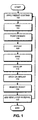
- FIG. 1 presents a flow chart illustrating the wafer fabrication process in accordance with an embodiment of the invention.
- the system starts by applying a photoresist layer to the top surface of a wafer (step 102).
- the system bakes the photoresist layer (step 104).
- the system positions a mask over the photoresist layer (step 106), and exposes the photoresist layer through the mask (step 108).
- multiple masks and/or exposures may be used in steps 106 and 108.
- the system optionally bakes the wafer again (step 114) before developing the photoresist layer (step 116).
- step 118 either a chemical etching or ion implantation step takes place (step 118) before the photoresist layer is removed (step 120). (Note that in the case of a lift-off process, a deposition can take place.) Finally, a new layer of material can be added and the process can be repeated for the new layer (step 122).
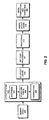
- FIG. 2 illustrates the process of creating a mask to be used in the wafer fabrication process described above in accordance with an embodiment of the invention.
- the process starts when a circuit designer produces a design 202 in VHDL, or some other hardware description language.
- VHDL is an acronym for VHSIC Hardware Description Language.
- VHSIC is a Department of Defense acronym that stands for very high-speed integrated circuits.
- the VHDL standard has been codified in Institute for Electrical and Electronic Engineers (IEEE) standard 1076-1993.
- Design 202 then feeds through a layout system 203 that performs a number of functions, such as synthesis 204, placement and routing 206 and verification 208.
- the result is an integrated circuit (IC) layout 210, which is in the form of a specification expressed in a format such as the hierarchical GDSII format.
- IC layout 210 then passes into RET post-processing system 211, which can perform resolution enhancement techniques (RETs) to facilitate printing of the IC layout 210 on the finished wafer.
- RET resolution enhancement techniques
- the IC layout 210 can be processed for RET such as phase shifting (e.g. alternating aperture dark field phase shifting) followed by OPC to compensate for proximity effects that arise during the wafer production process.
- the output of the RET post-processing system 211 feeds into fracturing process 212, which fractures the layout for subsequent mask-writing operations. This can be accomplished using any one of a number of well-known mask fracturing techniques.
- the output of fracturing process 212 is a new IC layout 218.
- New IC layout 218 subsequently passes into mask fabrication and inspection processes 220.
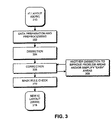
- FIG. 3 illustrates the process of generating a mask to be used in fabricating an integrated circuit in accordance with an embodiment of the invention. This flow chart describes in more detail some of the operations performed during step 211 of the flow chart illustrated in FIG. 2.
- the system starts with an IC layout 210 in GDSII format, and performs data preparation and preprocessing operations on the layout, which can include various operations, such as applying biases and identifying gates (step 302).
- the system performs a dissection operation to divide figures in the layout into segments for OPC purposes (step 304).
- the system performs the OPC operation on the segmented layout (step 306). If necessary, the system performs an additional dissection on "problem areas" in the layout that are not converging properly during the OPC process (step 308).
- the additional dissection can also involve reducing the number of segments in areas that prove to be simpler to correct than predicted.
- the system performs a mask rule check (MRC) operation to verify that the mask adheres to design rules before generating the new IC layout 218 (step 310).
- MRC mask rule check
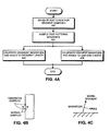
- FIG. 4A presents a flow chart illustrating how modeled intensity gradients are used in generating a segmentation in accordance with an embodiment of the invention. This flow chart describes in more detail some of the operations performed during step 211 of the flow chart illustrated in FIG. 2. The segmentations are in turn used during the dissection step 304 illustrated in FIG. 3.
- a calibrated choice of segment length can be made for any gradient value. This process involves creating test sets comprising optically significant but varying patterns, and then studying the gradient characteristics of the various features.
- the first step in this process is to develop an adequate test case to understand the implications of varying gradients (step 402). Note that the test set should include areas with known varying optical properties, but need not be particularly large.
- gradient values for a specific model may be explored.
- An understanding of gradient characteristics is obtained by sampling the gradient's angle and magnitude at various locations throughout the test set (step 404). To do this, a fine sampling of the gradient along all edges of all the test polygons is performed at a sampling frequency of 50 nm or smaller.
- a single gradient can be determined by taking four samples. Two of these samples are taken at tangential points along the edge, while the two other samples are taken along a normal to the edge. These four samples are used to compute tangential and normal components of the intensity gradient, which are combined to form the intensity gradient, which can be specified by a magnitude and an angle. Also note that it is possible to take fewer samples or more than four samples to determine a gradient. The output magnitude and angle are then correlated to correction complexity by investigating the sample segment movement when the test set is corrected in an unconstrained fashion using the model. (Note a number of different ways to sample a gradient are commonly known, so the above-described technique is just an example of one method.)
- FIG. 7 illustrates this concept, where area 701 has a correction shift variation between each sampled segment and area 704 has no correction shift variation between segments.
- the areas with a greater number of shifts need finer (smaller) correction segments, while those with small or no correction shifts between segments can have infinitely long segments.
- the gradient angle and magnitude data can be mapped to them. This mapping can be used to calibrate a gradient angle to a segment length (step 406). It can also be used to calibrate a gradient magnitude to a choice of a specific segmentation for a line-end (step 408).
- the system can use the calibrated segment lengths and line-end choices while performing the dissection operations discussed above with respect to steps 304 and 308 of FIG. 3.
- FIG. 5 presents a plot of gradient angle and magnitude versus pitch for the middle segment of a nested 4800 nm line.
- This is a one dimensional correction (ID) correction region that has special properties.
- the plot exhibits no tangential slope component, but comprises significant normal slope variation, which results in a constant ⁇ 90° angle but a varying magnitude.
- the magnitude appears to be sensitive to coherence effects.
- a series of nested segments at a distance greater than ambit from any two-dimensional feature will have the same correction shift within error for a given pitch.
- the information necessary to make segmentation choices is completely contained within the gradient angle for one dimensional correction regions. This indicates that shorter correction segments are necessary as more tangential gradient component relative to the normal gradient component is present on a segment. As two dimensional features are dissected, the angle and magnitude may be used together to decide dissection lengths.
- a similar process can be used for selecting a pre-defined segmentation for a line-end.
- the system can select between a line extension correction and a dog-ear serif correction.
- the two correction features are illustrated in FIGs 6A and 6B.
- a dog-ear serif correction divides the line-end into three correction segments of length W nm, and also divides the adjacent edges into short segments designated by run length of X nm.
- a line-end extension correction uses a single segment of length Y nm on the line-end, and Z nm segments on the edges adjacent to the line-end. When properly placed, there is little correction performance difference between the two features, but a significant segment count reduction when using the line-extension correction. Note that the segment lengths W , X , Y and Z can be varied based on design, desire, and process.
- a gradient magnitude at the line-end center can be used.
- coherence is relevant to the type of structure used during correction.
- the gradient magnitude for an isolated long line can be used to determine the trigger point for a change between a line-extension correction and a dog-ear serif correction.
- the isolated line case is a low mask error enhancement factor (MEEF) case where a correction such as a line-extension should perform well.
- MEEF mask error enhancement factor
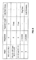
- FIG. 7 illustrates the process for mapping gradient angles to dissection length requirements. Example results of this effort are presented in the table which appears in FIG. 8.
- FIG. 7 illustrates a pattern prior to correction, with post-correction edge wire frame diagrams.
- the area highlighted in region 701 has large correction shifts applied to each correction and inspection of the gradient angles reveals angles from 45 to 75 degrees and 105 and 135 degrees.
- the correction in area 702 contrasts with that in area 701, revealing almost no variation in the correction shift applied over the regions.
- the gradient angle is checked over this region, it is found to move between approximately 90.1 and 89.9 degrees. (Note, the angle values in these examples may change based on need and are only illustrative.)
- Areas 703 and 704 are more marginal cases, where the potential for some longer segments exist, but variation is necessary to produce an adequate correction.
- the gradient angle varied from 85 to 95 degrees and the segments had small correction changes over several segments.
- the gradient angle was between 80 and 100 degrees, but it had significantly more correction shifts than were present in area 704. Therefore, area 703 angles were binned with area 701 angles, but area 704 was binned into its own angle region with an intermediate segment length.
- this lookup table (FIG. 8) is generated, it can then be refined during the correction process itself. For example, the exact transition values and segment lengths ( X and Y ) can be modified to refine the bin choices for specific patterns.
- the model-based dissection correction used in this example only performs model-based dissection on external line-end segments and one-dimensional correction segments. All other segments can be dissected using rules identical to those used for the rule-based dissection correction.
- the dissection length refers to the length of a single one-dimensional correction segment in rule-based dissection and the smallest possible correction segment in model-based dissection. (Note that in general segments can be dissected using model-based dissection, or a mix-and-match approach as discussed above.)
- FIGs. 9A-9C compare results of a model-based dissection against a rules-based dissection for a feature edge in accordance with one embodiment of the invention.
- FIG. 9A presents results of an initial gradient data-gathering step with vectors plotted at sampling points on the feature edge.
- FIG. 9B illustrates a segmentation of the feature edge, which uses rule-based dissection.
- FIG. 9C illustrates model-based segment sizing of the feature edge based upon intensity gradients in accordance with one embodiment of the invention. Note that the area with large angular deflections receives shorter segments, while those with perpendicular vectors are merged into one segment.
- the approach described herein can be applied to any type of lithographic process for fabricating semiconductor chips, including processes that make use of, deep-ultraviolet (DUV) radiation, extreme ultraviolet (EUV) radiation, X-rays, and electron beams, along with suitably modified masks.
- DUV deep-ultraviolet
- EUV extreme ultraviolet
- X-rays X-rays
- electron beams along with suitably modified masks.
- the approach described herein is not restricted to specific types of OPC, but can be generally applied to features related to a number of different correction or enhancement techniques, such as techniques that use phase shifting masks (PSM).
- PSM phase shifting masks
- a computer readable storage medium which may be any device or medium that can store code and/or data for use by a computer system.
- the transmission medium may include a communications network, such as the Internet.
- the electromagnetic wave form includes one or more of the ProteusTM and iN-TandemTM software programs, both from Synopsys, Inc., Mountain View, California.
Landscapes
- Physics & Mathematics (AREA)
- General Physics & Mathematics (AREA)
- Preparing Plates And Mask In Photomechanical Process (AREA)
- Design And Manufacture Of Integrated Circuits (AREA)
Abstract
Description
Claims (26)
- A method for dissecting a layout of an integrated circuit based on modeled intensity gradients to produce a segmentation for an optical proximity correction (OPC) process, comprising:receiving the layout for the integrated circuit;performing a model-based simulation on the layout to generate intensity gradients along edges of features in the layout; andgenerating a segmentation for edges in the layout based upon the intensity gradients, wherein the segmentation is used by a subsequent OPC process in generating corrections for the layout.
- The method of claim 1, wherein generating the segmentation involves:determining segment lengths for edges in the layout based upon the intensity gradients along the edges; andusing the segment lengths to dissect the edges in the layout, thereby generating the segmentation for the layout.
- The method of claim 2, wherein identifying a segment length for an edge involves using a predetermined association to map an intensity gradient angle (and possibly magnitude) to the segment length.
- The method of claim 1, wherein generating the segmentation involves selecting a segmentation for a line-end in the layout from a set of predetermined line-end segmentations based upon intensity gradients associated with the line-end.
- The method of claim 4, wherein the segmentation for the line-end is selected based upon a magnitude (and possibly angle) of an intensity gradient associated with the line-end.
- The method of any preceding claim, wherein performing the model-based simulation on the layout involves:dividing each edge in the layout into minimum-sized segments; andperforming a model-based simulation to determine an intensity gradient for each minimum-sized segment.
- The method of claim 6, wherein determining a gradient for a given minimum-sized segment involves performing a model-based simulation at two tangential points along the segment to determine a tangential component of the gradient.
- The method of claim 7, wherein determining the gradient for the given minimum-sized segment involves performing a model-based simulation at two points along a normal to the segment to determine a normal component of the gradient.
- The method of any preceding claim, further comprising performing the dissection again on problem areas in the layout after initial OPC operations take place.
- The method of any preceding claim, further comprising reducing the number of segments in areas that prove to be simpler to correct than predicted after initial OPC operations take place.
- The method of any preceding claim, wherein prior to receiving the layout, the method further comprises calibrating the association between gradients and segment lengths by:modeling an intensity gradient across a test pattern;identifying target regions in the test pattern that have a large amount of correction shift variation;mapping intensity gradients to the target regions;associating segment lengths with the target regions; andproducing an association between intensity gradients and segment lengths in the target regions, whereby the association is subsequently used in generating the segmentation for the layout.
- A computer program comprising instructions for implementing the method of any preceding claim.
- A computer-readable storage medium storing instructions that when executed by a computer cause the computer to perform a method for dissecting a layout of an integrated circuit based on modeled intensity gradients to produce a segmentation for an optical proximity correction (OPC) process, the method comprising:receiving the layout for the integrated circuit;performing a model-based simulation on the layout to generate intensity gradients along edges of features in the layout; andgenerating a segmentation for edges in the layout based upon the intensity gradients, wherein the segmentation is used by a subsequent OPC process in generating corrections for the layout.
- Apparatus that dissects a layout of an integrated circuit based on modeled intensity gradients to produce a segmentation for an optical proximity correction (OPC) process, comprising:a receiving mechanism configured to receive the layout for the integrated circuit;a model-based simulator configured to perform a model-based simulation on the layout to generate intensity gradients along edges of features in the layout; anda segmentation mechanism configured to generate a segmentation for edges in the layout based upon the intensity gradients, wherein the segmentation is used by a subsequent OPC process in generating corrections for the layout.
- The apparatus of claim 14, wherein the segmentation mechanism is configured to:determine segment lengths for edges in the layout based upon the intensity gradients along the edges; and touse the segment lengths to dissect the edges in the layout, thereby generating the segmentation for the layout.
- The apparatus of claim 15, wherein while identifying a segment length for an edge, the segmentation mechanism is configured to use a predetermined association to map an intensity gradient angle (and possibly magnitude) to the segment length.
- The apparatus of claim 14, wherein the segmentation mechanism is configured to select a segmentation for a line-end in the layout from a set of predetermined line-end segmentations based upon intensity gradients associated with the line-end.
- The apparatus of claim 17, wherein the segmentation mechanism is configured to select the segmentation for the line-end is selected based upon a magnitude (and possibly angle) of an intensity gradient associated with the line-end.
- The apparatus of any of claims 14 to 18, wherein the model-based simulator is configured to:divide each edge in the layout into minimum-sized segments; and toperform the model-based simulation to determine an intensity gradient for each minimum-sized segment.
- The apparatus of claim 19, wherein while determining a gradient for a given minimum-sized segment, the model-based simulator is configured to perform a model-based simulation at two tangential points along the segment to determine a tangential component of the gradient.
- The apparatus of claim 20, wherein while determining the gradient for the given minimum-sized segment, the model-based simulator is configured to perform a model-based simulation at two points along a normal to the segment to determine a normal component of the gradient.
- The apparatus of any of claims 14 to 21, wherein the segmentation mechanism is configured to perform the dissection again on problem areas in the layout after initial OPC operations take place.
- The apparatus of any of claims 14 to 22, wherein the segmentation mechanism is configured to reduce the number of segments in areas that prove to be simpler to correct than predicted after initial OPC operations take place.
- The apparatus of any of claims 14 to 23, further comprising a calibration mechanism configured to:model an intensity gradient across a test pattern;identify target regions in the test pattern that have a large amount of correction shift variation;map intensity gradients to the target regions;associate segment lengths with the target regions; and toproduce an association between intensity gradients and segment lengths in the target regions, whereby the association is subsequently used in generating the segmentation for the layout.
- An integrated circuit created through a process that dissects a layout for the integrated circuit based on modeled intensity gradients to produce a segmentation for an optical proximity correction (OPC) process, the process comprising:receiving the layout for the integrated circuit;performing a model-based simulation on the layout to generate intensity gradients along edges of features in the layout; andgenerating a segmentation for edges in the layout based upon the intensity gradients, wherein the segmentation is used by a subsequent OPC process in generating corrections for the layout.
- A mask for use in an optical lithography process for manufacturing an integrated circuit, wherein the mask is generated through a process that dissects a layout for the integrated circuit based on modeled intensity gradients to produce a segmentation for an optical proximity correction (OPC) process, the process comprising:receiving the layout for the integrated circuit;performing a model-based simulation on the layout to generate intensity gradients along edges of features in the layout; andgenerating a segmentation for edges in the layout based upon the intensity gradients, wherein the segmentation is used by a subsequent OPC process in generating corrections for the layout.
Applications Claiming Priority (2)
| Application Number | Priority Date | Filing Date | Title |
|---|---|---|---|
| US10/683,534 US7451068B2 (en) | 2003-10-10 | 2003-10-10 | Method and apparatus for generating an OPC segmentation based on modeled intensity gradients |
| US683534 | 2003-10-10 |
Publications (2)
| Publication Number | Publication Date |
|---|---|
| EP1522889A2 true EP1522889A2 (en) | 2005-04-13 |
| EP1522889A3 EP1522889A3 (en) | 2006-04-26 |
Family
ID=34314160
Family Applications (1)
| Application Number | Title | Priority Date | Filing Date |
|---|---|---|---|
| EP04256064A Ceased EP1522889A3 (en) | 2003-10-10 | 2004-09-30 | Method and apparatus for generating an OPC segmentation |
Country Status (2)
| Country | Link |
|---|---|
| US (1) | US7451068B2 (en) |
| EP (1) | EP1522889A3 (en) |
Families Citing this family (26)
| Publication number | Priority date | Publication date | Assignee | Title |
|---|---|---|---|---|
| US7080349B1 (en) * | 2004-04-05 | 2006-07-18 | Advanced Micro Devices, Inc. | Method of developing optimized optical proximity correction (OPC) fragmentation script for photolithographic processing |
| US7251807B2 (en) * | 2005-02-24 | 2007-07-31 | Synopsys, Inc. | Method and apparatus for identifying a manufacturing problem area in a layout using a process-sensitivity model |
| US7313780B2 (en) * | 2005-03-10 | 2007-12-25 | Chartered Semiconductor Manufacturing Ltd. | System and method for designing semiconductor photomasks |
| US7315999B2 (en) * | 2005-03-17 | 2008-01-01 | Synopsys, Inc. | Method and apparatus for identifying assist feature placement problems |
| US7743358B2 (en) * | 2005-04-29 | 2010-06-22 | Cadence Design Systems, Inc. | Apparatus and method for segmenting edges for optical proximity correction |
| KR100655428B1 (en) * | 2005-10-24 | 2006-12-08 | 삼성전자주식회사 | Optical proximity effect correction system and method |
| US7962868B2 (en) | 2005-10-28 | 2011-06-14 | Freescale Semiconductor, Inc. | Method for forming a semiconductor device using optical proximity correction for the optical lithography |
| US8370773B2 (en) * | 2006-08-16 | 2013-02-05 | Freescale Semiconductor, Inc. | Method and apparatus for designing an integrated circuit using inverse lithography technology |
| US20080178140A1 (en) * | 2007-01-18 | 2008-07-24 | United Microelectronics Corp. | Method for correcting photomask pattern |
| US8103984B1 (en) * | 2009-02-23 | 2012-01-24 | Cadence Design Systems, Inc. | System and method for compressed design phase contour data |
| US8321818B2 (en) * | 2009-06-26 | 2012-11-27 | International Business Machines Corporation | Model-based retargeting of layout patterns for sub-wavelength photolithography |
| US8146026B2 (en) * | 2009-11-17 | 2012-03-27 | International Business Machines Corporation | Simultaneous photolithographic mask and target optimization |
| US8230372B2 (en) * | 2009-12-03 | 2012-07-24 | International Business Machines Corporation | Retargeting for electrical yield enhancement |
| US8331646B2 (en) * | 2009-12-23 | 2012-12-11 | International Business Machines Corporation | Optical proximity correction for transistors using harmonic mean of gate length |
| US8415077B2 (en) | 2010-08-13 | 2013-04-09 | International Business Machines Corporation | Simultaneous optical proximity correction and decomposition for double exposure lithography |
| US8381153B2 (en) * | 2010-09-17 | 2013-02-19 | Taiwan Semiconductor Manufacturing Company, Ltd. | Dissection splitting with optical proximity correction and mask rule check enforcement |
| US8645876B2 (en) * | 2011-09-15 | 2014-02-04 | Globalfoundries Singapore Pte. Ltd. | Methodology for performing post layer generation check |
| US8589830B2 (en) | 2012-03-07 | 2013-11-19 | Taiwan Semiconductor Manufacturing Company, Ltd. | Method and apparatus for enhanced optical proximity correction |
| US8527916B1 (en) * | 2012-03-14 | 2013-09-03 | Taiwan Semiconductor Manufacturing Company, Ltd. | Dissection splitting with optical proximity correction to reduce corner rounding |
| US8627241B2 (en) * | 2012-04-16 | 2014-01-07 | Taiwan Semiconductor Manufacturing Company, Ltd. | Pattern correction with location effect |
| US8739080B1 (en) * | 2012-10-04 | 2014-05-27 | Taiwan Semiconductor Manufacturing Company, Ltd. | Mask error enhancement factor (MEEF) aware mask rule check (MRC) |
| US9189588B2 (en) | 2013-12-10 | 2015-11-17 | Taiwan Semiconductor Manufacturing Company, Ltd. | Polygon-based optical proximity correction |
| US9262578B2 (en) | 2014-04-25 | 2016-02-16 | Taiwan Semiconductor Manufacturing Company, Ltd. | Method for integrated circuit manufacturing |
| US9679100B2 (en) * | 2015-08-21 | 2017-06-13 | Taiwan Semiconductor Manufacturing Company, Ltd. | Environmental-surrounding-aware OPC |
| CN106599434A (en) * | 2016-12-07 | 2017-04-26 | 中国电子科技集团公司第四十七研究所 | Packaging structure anatomizing and reproducing method |
| CN106599433A (en) * | 2016-12-07 | 2017-04-26 | 中国电子科技集团公司第四十七研究所 | A system and method for anatomy and reproduction of encapsulated structures |
Family Cites Families (11)
| Publication number | Priority date | Publication date | Assignee | Title |
|---|---|---|---|---|
| US6467076B1 (en) * | 1999-04-30 | 2002-10-15 | Nicolas Bailey Cobb | Method and apparatus for submicron IC design |
| US6643616B1 (en) | 1999-12-07 | 2003-11-04 | Yuri Granik | Integrated device structure prediction based on model curvature |
| US6453457B1 (en) * | 2000-09-29 | 2002-09-17 | Numerical Technologies, Inc. | Selection of evaluation point locations based on proximity effects model amplitudes for correcting proximity effects in a fabrication layout |
| TWI285295B (en) * | 2001-02-23 | 2007-08-11 | Asml Netherlands Bv | Illumination optimization in lithography |
| US6792591B2 (en) * | 2001-02-28 | 2004-09-14 | Asml Masktools B.V. | Method of identifying an extreme interaction pitch region, methods of designing mask patterns and manufacturing masks, device manufacturing methods and computer programs |
| US20030061587A1 (en) * | 2001-09-21 | 2003-03-27 | Numerical Technologies, Inc. | Method and apparatus for visualizing optical proximity correction process information and output |
| US7082596B2 (en) * | 2002-11-27 | 2006-07-25 | Synopsys, Inc. | Simulation-based selection of evaluation points for model-based optical proximity correction |
| US7124394B1 (en) * | 2003-04-06 | 2006-10-17 | Luminescent Technologies, Inc. | Method for time-evolving rectilinear contours representing photo masks |
| US7010764B2 (en) * | 2003-04-14 | 2006-03-07 | Takumi Technology Corp. | Effective proximity effect correction methodology |
| US7043712B2 (en) * | 2003-09-09 | 2006-05-09 | International Business Machines Corporation | Method for adaptive segment refinement in optical proximity correction |
| US6978438B1 (en) * | 2003-10-01 | 2005-12-20 | Advanced Micro Devices, Inc. | Optical proximity correction (OPC) technique using generalized figure of merit for photolithograhic processing |
-
2003
- 2003-10-10 US US10/683,534 patent/US7451068B2/en not_active Expired - Lifetime
-
2004
- 2004-09-30 EP EP04256064A patent/EP1522889A3/en not_active Ceased
Also Published As
| Publication number | Publication date |
|---|---|
| US20050081179A1 (en) | 2005-04-14 |
| US7451068B2 (en) | 2008-11-11 |
| EP1522889A3 (en) | 2006-04-26 |
Similar Documents
| Publication | Publication Date | Title |
|---|---|---|
| US7451068B2 (en) | Method and apparatus for generating an OPC segmentation based on modeled intensity gradients | |
| US7624369B2 (en) | Closed-loop design for manufacturability process | |
| US11061318B2 (en) | Lithography model calibration | |
| EP1677221B1 (en) | Method and apparatus for placing assist features in a layout | |
| US8413081B2 (en) | Method for process window optimized optical proximity correction | |
| CN102566254B (en) | Methods for arranging sub-resolution auxiliary feature in mask layout and method for determining one or more positions of features | |
| US7882480B2 (en) | System and method for model-based sub-resolution assist feature generation | |
| US7475383B2 (en) | Method of fabricating photo mask | |
| US8843859B2 (en) | Layout content analysis for source mask optimization acceleration | |
| US20100269084A1 (en) | Visibility and Transport Kernels for Variable Etch Bias Modeling of Optical Lithography | |
| JP2004246223A (en) | Mask correction method | |
| US8473878B2 (en) | Lithographically enhanced edge determination | |
| KR20090085651A (en) | Printability Verification by Incremental Modeling Precision | |
| JP2003525470A (en) | Method and apparatus for mixed mode optical proximity correction | |
| US10732499B2 (en) | Method and system for cross-tile OPC consistency | |
| US8533637B2 (en) | Retargeting based on process window simulation | |
| US7082596B2 (en) | Simulation-based selection of evaluation points for model-based optical proximity correction | |
| US7251806B2 (en) | Model-based two-dimensional interpretation filtering | |
| US20090210838A1 (en) | Interpolation distance for layout desing data correction model | |
| US8619236B2 (en) | Determining lithographic set point using optical proximity correction verification simulation | |
| US20100082313A1 (en) | Optical Lithographic Process Model Calibration | |
| TW202328799A (en) | Mask synthesis integrating mask fabrication effects and wafer lithography effects | |
| WO2007048442A1 (en) | Method for forming a semiconductor device using optical proximity correction for the optical lithography | |
| Rodriguez | Melvin, III (45) Date of Patent: Nov. 11, 2008 | |
| US20250102921A1 (en) | Adaptive target control for curvilinear optical proximity correction (opc) |
Legal Events
| Date | Code | Title | Description |
|---|---|---|---|
| PUAI | Public reference made under article 153(3) epc to a published international application that has entered the european phase |
Free format text: ORIGINAL CODE: 0009012 |
|
| AK | Designated contracting states |
Kind code of ref document: A2 Designated state(s): AT BE BG CH CY CZ DE DK EE ES FI FR GB GR HU IE IT LI LU MC NL PL PT RO SE SI SK TR |
|
| AX | Request for extension of the european patent |
Extension state: AL HR LT LV MK |
|
| PUAL | Search report despatched |
Free format text: ORIGINAL CODE: 0009013 |
|
| RIC1 | Information provided on ipc code assigned before grant |
Ipc: G03F 1/14 20060101ALI20060217BHEP Ipc: G03F 7/20 20060101AFI20060217BHEP |
|
| AK | Designated contracting states |
Kind code of ref document: A3 Designated state(s): AT BE BG CH CY CZ DE DK EE ES FI FR GB GR HU IE IT LI LU MC NL PL PT RO SE SI SK TR |
|
| AX | Request for extension of the european patent |
Extension state: AL HR LT LV MK |
|
| 17P | Request for examination filed |
Effective date: 20061011 |
|
| AKX | Designation fees paid |
Designated state(s): DE FR IT NL |
|
| 17Q | First examination report despatched |
Effective date: 20080401 |
|
| STAA | Information on the status of an ep patent application or granted ep patent |
Free format text: STATUS: THE APPLICATION HAS BEEN REFUSED |
|
| 18R | Application refused |
Effective date: 20150419 |