EP1521380A1 - Apparatus and method for reducing cross-talk between transmitted signals - Google Patents
Apparatus and method for reducing cross-talk between transmitted signals Download PDFInfo
- Publication number
- EP1521380A1 EP1521380A1 EP03022147A EP03022147A EP1521380A1 EP 1521380 A1 EP1521380 A1 EP 1521380A1 EP 03022147 A EP03022147 A EP 03022147A EP 03022147 A EP03022147 A EP 03022147A EP 1521380 A1 EP1521380 A1 EP 1521380A1
- Authority
- EP
- European Patent Office
- Prior art keywords
- signal
- transmission path
- time period
- delayed
- delay time
- Prior art date
- Legal status (The legal status is an assumption and is not a legal conclusion. Google has not performed a legal analysis and makes no representation as to the accuracy of the status listed.)
- Granted
Links
- 238000000034 method Methods 0.000 title claims description 11
- 230000005540 biological transmission Effects 0.000 claims abstract description 73
- 230000003111 delayed effect Effects 0.000 claims abstract description 34
- 230000000630 rising effect Effects 0.000 claims abstract description 16
- 230000001052 transient effect Effects 0.000 claims description 2
- 238000010586 diagram Methods 0.000 description 11
- 230000000694 effects Effects 0.000 description 7
- 230000000875 corresponding effect Effects 0.000 description 2
- 230000002596 correlated effect Effects 0.000 description 1
- 230000001934 delay Effects 0.000 description 1
- 230000003071 parasitic effect Effects 0.000 description 1
- 238000005070 sampling Methods 0.000 description 1
- 230000008054 signal transmission Effects 0.000 description 1
Images



Classifications
-
- H—ELECTRICITY
- H04—ELECTRIC COMMUNICATION TECHNIQUE
- H04B—TRANSMISSION
- H04B3/00—Line transmission systems
- H04B3/02—Details
- H04B3/20—Reducing echo effects or singing; Opening or closing transmitting path; Conditioning for transmission in one direction or the other
- H04B3/23—Reducing echo effects or singing; Opening or closing transmitting path; Conditioning for transmission in one direction or the other using a replica of transmitted signal in the time domain, e.g. echo cancellers
-
- H—ELECTRICITY
- H05—ELECTRIC TECHNIQUES NOT OTHERWISE PROVIDED FOR
- H05K—PRINTED CIRCUITS; CASINGS OR CONSTRUCTIONAL DETAILS OF ELECTRIC APPARATUS; MANUFACTURE OF ASSEMBLAGES OF ELECTRICAL COMPONENTS
- H05K1/00—Printed circuits
- H05K1/02—Details
- H05K1/0213—Electrical arrangements not otherwise provided for
- H05K1/0216—Reduction of cross-talk, noise or electromagnetic interference
Definitions
- the present invention relates to an apparatus and a method for transmitting a first and a second signal on a first and a second transmission path, and in particular, to a cross-talk compensation for transmission paths on a printed circuit board.
- Cross-talk between neighboring transmission lines is a significant problem for transferring information on the transmission lines from a transmitter to a receiver.
- neighboring transmission lines are coupled by a parasitic capacitance and inductance.
- simultaneous switching signals on neighboring transmission lines influence each other.
- Simultaneously rising edges or falling edges on neighboring transmission lines result in a shorter propagation time of both signal edges.
- a computer memory subsystem comprises a plurality of multi-line parallel busses. On an address bus and a data bus of a computer memory subsystem, all signals are driven simultaneously at the transmitter side. This increases the effect of cross-talk. Cross-talk is further increased as neighboring transmission lines often run in parallel due to a limited available space on a printed circuit board and due to routing constrains.
- Fig. 3 shows a schematic view of a multi-line parallel bus which comprises three neighboring transmission lines.
- a first 302, a second 304 and a third 306 signal are driven by a first 312, a second 314 and a third 316 driver on a first 322, a second 324 and a third 326 transmission line.
- the signals 302, 304, 306 are received by a first 332, a second 334 and a third 336 receiver.
- Cross-talk is increased by a parallel routing of neighboring transmission lines.
- the transmission lines 322, 324, 326 are printed circuit board transmission lines which have a length of 101 mm, a width of 0.1 mm, a spacing between neighboring transmission lines of 0.1 mm, a thickness of 0.046 mm, a distance to a ground layer (not shown) of 0.087 mm, a dielectric permittivity of 4.5 and a characteristic trace impedance of approximately 60 ⁇ .
- the drivers 312, 314, 316 each comprise a 40 ⁇ resistor, a high level of 1.5 V, a low level of 0 V and a rise and fall time of 250 ps.
- the signals 302, 304, 306 each carry a 256 bit non-correlated pseudo-random bit sequence at a bit rate of 1.6 Gbit/s.
- the receiver 332, 334, 336 each comprise a 60 ⁇ resistor connected to a middle level voltage of 1.5 V.
- Fig. 4 shows an eye diagram 440 of the second signal 304 of Fig. 3, taken at the place marked by an "A".
- the eye diagram 440 shows a falling edge 450 and a rising edge 460 of the second signal which are not influenced by the neighboring signals shown in Fig. 3. Further, the eye diagram 440 shows influenced rising edges 450a, 450b and influenced falling edges 460a, 460b of the second signal.
- the uninfluenced edges 450, 460 relate to a state, in which neighboring signal lines are not switching or are both switching in an opposite direction.
- the influenced edges 450a, 460a arrive earlier than the uninfluenced edges 450, 460. This happens as the neighboring signals switch in the same direction as the second signal.
- the influenced edges 450b, 460b arrive later than the uninfluenced edges 450, 460. This happens if the neighboring signals switch in an opposite direction than the second signal.
- An opening 470 of the eye defines a time between two switching events, in which the state of the second signal is defined and a valid value can be sampled by a receiver. As can be seen, the opening 470 of the eye is reduced due to the influenced edges 450a, b, 460a, b. In this embodiment, the opening of the eye has a duration of 500 ps.
- the opening 470 of the eye becomes too small for securely sampling the second signal.
- cross-talk on the transmission lines has to be reduced.
- cross-talk is reduced by increasing a spacing between neighboring transmission lines or by including additional grounded guard traces. Due to space limitations and routing constrains, these methods are often not feasible.
- the present invention provides an apparatus for transmitting a first and a second signal on a first and a second transmission path which are arranged such that a cross-talk between the transmission paths takes place when the first and second signals are transmitted on the first and second transmission path, said apparatus comprising:
- the present invention further provides a method for transmitting a first and a second signal on a first and a second signal transmission path which are arranged such that the cross-talk between the transmission paths takes place when the first and second signals are transmitted on the first and second transmission path, the method comprising the steps of:
- the apparatus for transmitting a first and a second signal comprises additional means for providing separate strobe-signals which allow a receiver to latch the transmitted signals.
Landscapes
- Engineering & Computer Science (AREA)
- Computer Networks & Wireless Communication (AREA)
- Signal Processing (AREA)
- Dc Digital Transmission (AREA)
- Cable Transmission Systems, Equalization Of Radio And Reduction Of Echo (AREA)
Abstract
Description
- The present invention relates to an apparatus and a method for transmitting a first and a second signal on a first and a second transmission path, and in particular, to a cross-talk compensation for transmission paths on a printed circuit board.
- Cross-talk between neighboring transmission lines is a significant problem for transferring information on the transmission lines from a transmitter to a receiver. On a printed circuit board, neighboring transmission lines are coupled by a parasitic capacitance and inductance. Thus, simultaneous switching signals on neighboring transmission lines influence each other. Simultaneously rising edges or falling edges on neighboring transmission lines result in a shorter propagation time of both signal edges. Opposite edges, this is a falling and a rising edge, on neighboring transmission lines result in a longer propagation time. Even if all transmission lines have a same length and a same characteristic impedance, the simultaneously driven signals do not arrive simultaneously at the receiver. The arrival time of the signals depends on the state of the neighboring transmission lines.
- A computer memory subsystem comprises a plurality of multi-line parallel busses. On an address bus and a data bus of a computer memory subsystem, all signals are driven simultaneously at the transmitter side. This increases the effect of cross-talk. Cross-talk is further increased as neighboring transmission lines often run in parallel due to a limited available space on a printed circuit board and due to routing constrains.
- If a random bit sequence is driven on two neighboring transmission lines, a part of the received bits will be delayed and another part will arrive earlier. This results in a timing uncertainty of the transmitted bits at the receiver. In high data rate designs, the timing uncertainty makes it more difficult to receive the bits. Due to the timing uncertainty a data valid interval becomes very small, especially if several neighboring traces switch simultaneously with a rising or simultaneously with a falling edge.
- Fig. 3 shows a schematic view of a multi-line parallel bus which comprises three neighboring transmission lines. A first 302, a second 304 and a third 306 signal are driven by a first 312, a second 314 and a third 316 driver on a first 322, a second 324 and a third 326 transmission line. The
signals - In multi-line busses which are typically for memory systems, Cross-talk is increased by a parallel routing of neighboring transmission lines.
- In the embodiment shown in Fig. 3, the
transmission lines - The
drivers signals receiver - Fig. 4 shows an eye diagram 440 of the
second signal 304 of Fig. 3, taken at the place marked by an "A". - The eye diagram 440 shows a falling
edge 450 and a risingedge 460 of the second signal which are not influenced by the neighboring signals shown in Fig. 3. Further, the eye diagram 440 shows influenced rising edges 450a, 450b and influenced falling edges 460a, 460b of the second signal. - The
uninfluenced edges - The influenced edges 450a, 460a arrive earlier than the
uninfluenced edges uninfluenced edges - An
opening 470 of the eye defines a time between two switching events, in which the state of the second signal is defined and a valid value can be sampled by a receiver. As can be seen, the opening 470 of the eye is reduced due to the influenced edges 450a, b, 460a, b. In this embodiment, the opening of the eye has a duration of 500 ps. - Especially in high data rate designs, the opening 470 of the eye becomes too small for securely sampling the second signal. In order to increase the opening 470 of the eye, cross-talk on the transmission lines has to be reduced. According to the prior art, cross-talk is reduced by increasing a spacing between neighboring transmission lines or by including additional grounded guard traces. Due to space limitations and routing constrains, these methods are often not feasible.
- It is the object of the present invention, to provide an apparatus and a method for transmitting a first and a second signal on neighboring transmission paths which compensates cross-talk between the first and the second signal in a cost- and space-effective manner.
- This object is achieved by an apparatus for transmitting a first and a second signal according to claim 1 and a method for transmitting a first and a second signal according to claim 9.
- The present invention provides an apparatus for transmitting a first and a second signal on a first and a second transmission path which are arranged such that a cross-talk between the transmission paths takes place when the first and second signals are transmitted on the first and second transmission path, said apparatus comprising:
- a first means for driving the first signal on the first transmission path;
- a means for delaying the second signal by a delay time period and for providing a delayed signal;
- a second means for driving the delayed signal on the second transmission path; wherein the delay time period is such that rising and falling edges of the first signal and the delayed signal do not coincide.
-
- The present invention further provides a method for transmitting a first and a second signal on a first and a second signal transmission path which are arranged such that the cross-talk between the transmission paths takes place when the first and second signals are transmitted on the first and second transmission path, the method comprising the steps of:
- driving the first signal on the first transmission path;
- delaying the second signal by a delay time period and providing a delayed signal;
- driving the delayed signal on the second transmission path; wherein the delay time period is such that rising and falling edges of the first signal and the delayed signal do not coincide.
-
- The present invention is based on the finding that cross-talk between two neighboring transmission paths can be compensated by delaying one of the two signals such that the two signals switch asynchronously.
- The proposed method for cross-talk compensation can be advantageously used in a multi-line parallel bus. It does not require additional routing space and does not cause additional costs as a necessary delay-line can be implemented in an integrated circuit without additional effort. Alternatively, the proposed method allows to reduce a spacing between neighboring transmission paths without increasing the effect of cross-talk.
- According to a further embodiment of the present invention, the apparatus for transmitting a first and a second signal comprises additional means for providing separate strobe-signals which allow a receiver to latch the transmitted signals.
- Preferred embodiments of the present invention are described herein after, making reference to the append drawings.
- Fig. 1
- shows a schematic view of an apparatus for transmitting a first and a second signal on a first and a second transmission path;
- Fig. 2
- shows an eye diagram of a signal shown in Fig. 1;
- Fig. 3
- shows a schematic view of an apparatus for transmitting a first and a second signal on a first and a second transmission path according to the prior art; and
- Fig. 4
- shows an eye diagram of a signal shown in Fig. 3.
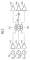
- Fig. 1 shows a schematic view of an apparatus for transmitting a first and a second signal on a first and a second transmission path. This embodiment comprises a
first signal 102, asecond signal 104 and athird signal 106. The first and thethird signal second signal 104. Thesecond signal 104 is connected to adelay line 108 which delays thesecond signal 104 by a defined delay time period and provides a delayed signal 104'. The first signals 102, 106 and the delayed signal 104' are driven by afirst driver 112, asecond driver 114 and athird driver 116 on afirst transmission path 122, asecond transmission path 124 and athird transmission path 126. Thetransmission paths first receiver 132, asecond receiver 134 and athird receiver 136 which sample the corresponding transmittedsignals signal 137, a second receivedsignal 138 and a thirdreceived signal 139. In this embodiment, the first and the thirdreceived signals third delay line - In the present embodiment, the
drivers receivers delay lines transmission paths signals drivers transmission paths receivers - According to the invention, the
second signal 104 is delayed by thedelay line 108 by a delay period such that the edges of the neighboringsignals first signals second signal 104. If the relationship is not known or is changing, a clock signal (not shown) is used for synchronizing thefirst signals second signal 104. - In order to align the received signals 137, 138, 139, the
receivers delay lines first signals delay line 108 at the transmitter side. - An eye diagram 240 of the delayed signal 104' shown in Fig. 1 at the place marked by an "A" is shown in Fig. 2. The eye diagram 240 shows a falling
edge 250 and a risingedge 260 of the delayed signal. As can be seen from Fig. 2, the embodiment as described in Fig. 1 prevents an influence of the neighboring transmission lines on theedges opening 270 of the eye has a maximum width. In this embodiment theopening 270 of the eye has a duration of 612 ps which is longer than the opening of the influenced eye diagram shown in Fig. 4. - In this embodiment, the first and second signals switch periodically with a bit-time period and the delay line period is such that the second signal is delayed by half a bit time. Therefore, edges of the first signals do not effect the delayed signal while it is switching but while it is in a stable high or
low state 280. Preferably, a voltage margin in thestable state 280 is such that a ring-back due to the cross-talk effect does not effect a signal integrity. - According to a further embodiment, the second signal is not delayed by a half bit-time period but by a shorter delay time period which equals a transient time period of the first signal. Thus, in a low data rate design, it might be unnecessary to delay the first signal at the receiver side.
- According to a further embodiment, the apparatus for transmitting a first and a second signal comprises strobe-signals. A first strobe-signal is driven correspondingly to the first signal and a second strobe-signal is driven correspondingly to the second signal. The strobe-signal indicate a switching of the first signal and the delayed signal. Thus, the delay lines on the receiver side are not necessary and the data rate can be increased.
- In an embodiment comprising a multi-line parallel bus, every second transmission path signal is delayed. The multi-line parallel bus can be part of a memory sub system or be part of any other design which comprises at least to parallel transmission paths. The transmission paths are not limited to lines on a printed circuit board but can be any transmission paths on which transmitted signals effect each other on neighboring transmission paths.
-
- 102
- first signal
- 104
- second signal
- 106
- third signal
- 108
- delay line
- 112
- first driver
- 114
- second driver
- 116
- third driver
- 122
- first transmission path
- 124
- second transmission path
- 126
- third transmission path
- 132
- first receiver
- 134
- second receiver
- 136
- third receiver
- 138, 139
- receiver delay lines
- 240
- eye diagram
- 250
- falling edge
- 260
- rising edge
- 270
- opening of the eye diagram
- 280
- stable states
- 302, 304, 306
- first, second, third signals
- 312, 314, 316
- first, second, third drivers
- 322, 324, 326
- first, second, third transmission lines
- 332, 334, 336
- first, second, third receivers
- 440
- eye diagram
- 450
- uninfluenced rising edge
- 460
- uninfluenced falling edge
- 450a, b
- influenced rising edges
- 460a, b
- influenced falling edges
- 470
- opening of the eye
Claims (9)
- Apparatus for transmitting a first signal (102) and a second signal (104) on a first transmission path (122) and a second transmission path (124) which are arranged such that a cross-talk between the transmission paths takes place when the first and the second signal are transmitted on the first and second transmission path, said apparatus comprising:wherein the delay time period is such that rising and falling edges of the first signal do not coincide with rising (260) and falling (250) edges of the delayed signal.a first means (112) for driving the first signal on the first transmission path;a means (108) for delaying the second signal by a delay time period and for providing a delayed signal (104');a second means (114) for driving the delayed signal on the second transmission path;
- Apparatus according to claim 1, further comprising a clock signal for synchronizing the first signal and the second signal.
- Apparatus according to one of claims 1 or 2, further comprising a first and a second means (132, 134) for receiving the transmitted first and the delayed signal and for providing a received first signal (137; 139) and a received second signal (138); and
a means for delaying the received first signal by the delay time period. - Apparatus according to one of claims 1 to 3, wherein the first and the second signals (102, 104) are driven periodically with a bit time period and wherein the delay time period is such that the delayed signal (104') is driven between one third or two thirds of the bit time period after the first signal is driven.
- Apparatus according to one of claims 1 to 3, wherein the delay time period is such that the delayed signal is driven after a transient effect of the first signal.
- Apparatus according to one of claims 1 to 5, further comprising a first and a second means for driving a first and a second strobe-signal, wherein the first strobe-signal corresponds to the first signal and wherein the second strobe-signal corresponds to the delayed signal.
- Apparatus according to one of claims 1 to 6, wherein the means for delaying is a delay line.
- Apparatus according to one of claims 1 to 7, wherein the first and the second transmission paths are printed circuit board transmission lines.
- Method for transmitting a first and a second signal on a first and a second transmission path which are arranged such that a cross-talk between the transmission paths takes place when the first and second signal are transmitted on the first and the second transmission path, said method comprising the steps of:wherein the delay time period is such that rising and falling edges of the first signal do not coincide with rising and falling edges of the delayed signal.driving the first signal on the first transmission path;delaying the second signal by a delay time period and providing a delayed signal;driving the delayed signal on the second transmission path;
Priority Applications (3)
| Application Number | Priority Date | Filing Date | Title |
|---|---|---|---|
| EP03022147A EP1521380B1 (en) | 2003-09-30 | 2003-09-30 | Apparatus and method for reducing cross-talk between transmitted signals |
| DE60319703T DE60319703T2 (en) | 2003-09-30 | 2003-09-30 | Apparatus and method for reducing crosstalk between transmission signals |
| US10/952,563 US20050259826A1 (en) | 2003-09-30 | 2004-09-28 | Apparatus and method for transmitting signals |
Applications Claiming Priority (1)
| Application Number | Priority Date | Filing Date | Title |
|---|---|---|---|
| EP03022147A EP1521380B1 (en) | 2003-09-30 | 2003-09-30 | Apparatus and method for reducing cross-talk between transmitted signals |
Publications (2)
| Publication Number | Publication Date |
|---|---|
| EP1521380A1 true EP1521380A1 (en) | 2005-04-06 |
| EP1521380B1 EP1521380B1 (en) | 2008-03-12 |
Family
ID=34306807
Family Applications (1)
| Application Number | Title | Priority Date | Filing Date |
|---|---|---|---|
| EP03022147A Expired - Lifetime EP1521380B1 (en) | 2003-09-30 | 2003-09-30 | Apparatus and method for reducing cross-talk between transmitted signals |
Country Status (3)
| Country | Link |
|---|---|
| US (1) | US20050259826A1 (en) |
| EP (1) | EP1521380B1 (en) |
| DE (1) | DE60319703T2 (en) |
Families Citing this family (2)
| Publication number | Priority date | Publication date | Assignee | Title |
|---|---|---|---|---|
| US9369308B2 (en) | 2013-11-07 | 2016-06-14 | International Business Machines Corporation | Signal transmission reducing coupling caused delay variation |
| CN116491852B (en) * | 2023-05-12 | 2026-04-07 | 深圳拓邦股份有限公司 | A communication anti-interference method and a handheld vacuum cleaner |
Citations (3)
| Publication number | Priority date | Publication date | Assignee | Title |
|---|---|---|---|---|
| EP1085672A2 (en) * | 1999-08-23 | 2001-03-21 | Nec Corporation | Method and system for minimising crosstalk |
| US20020199049A1 (en) * | 2001-06-20 | 2002-12-26 | Mitsubishi Denki Kabushiki Kaisha | Signal bus arrangement |
| US20030038664A1 (en) * | 2001-08-21 | 2003-02-27 | Nec Corporation | Semiconductor integrated circuit |
Family Cites Families (3)
| Publication number | Priority date | Publication date | Assignee | Title |
|---|---|---|---|---|
| FR2818838A1 (en) * | 2000-12-21 | 2002-06-28 | Cit Alcatel | ADJUSTABLE DIFFERENTIAL GROUP DELAY GENERATOR AND POLARIZATION DISPERSION COMPENSATOR INCORPORATING SAME |
| US20030081709A1 (en) * | 2001-10-30 | 2003-05-01 | Sun Microsystems, Inc. | Single-ended IO with dynamic synchronous deskewing architecture |
| TWI256542B (en) * | 2002-03-22 | 2006-06-11 | Via Tech Inc | Data latch time control method and device |
-
2003
- 2003-09-30 DE DE60319703T patent/DE60319703T2/en not_active Expired - Fee Related
- 2003-09-30 EP EP03022147A patent/EP1521380B1/en not_active Expired - Lifetime
-
2004
- 2004-09-28 US US10/952,563 patent/US20050259826A1/en not_active Abandoned
Patent Citations (3)
| Publication number | Priority date | Publication date | Assignee | Title |
|---|---|---|---|---|
| EP1085672A2 (en) * | 1999-08-23 | 2001-03-21 | Nec Corporation | Method and system for minimising crosstalk |
| US20020199049A1 (en) * | 2001-06-20 | 2002-12-26 | Mitsubishi Denki Kabushiki Kaisha | Signal bus arrangement |
| US20030038664A1 (en) * | 2001-08-21 | 2003-02-27 | Nec Corporation | Semiconductor integrated circuit |
Also Published As
| Publication number | Publication date |
|---|---|
| US20050259826A1 (en) | 2005-11-24 |
| DE60319703D1 (en) | 2008-04-24 |
| EP1521380B1 (en) | 2008-03-12 |
| DE60319703T2 (en) | 2009-03-19 |
Similar Documents
| Publication | Publication Date | Title |
|---|---|---|
| EP0940758B1 (en) | Serial bus speed-up circuit | |
| JPH069040B2 (en) | Data processing device | |
| IE54982B1 (en) | Communication bus | |
| US6625206B1 (en) | Simultaneous bidirectional data transmission system and method | |
| US5101347A (en) | System for reducing skew in the parallel transmission of multi-bit data slices | |
| EP0687399B1 (en) | BiCMOS differential delay element with constant pulse width | |
| US6346830B1 (en) | Data input/output circuit and interface system using the same | |
| US6657460B2 (en) | Spatially filtered data bus drivers and receivers and method of operating same | |
| US6249142B1 (en) | Dynamically terminated bus | |
| US6697974B2 (en) | Method and apparatus for adaptively compensating skews during data transmission on a bus | |
| US6681338B1 (en) | Method and system for reducing signal skew by switching between multiple signal routing layers | |
| EP1521380A1 (en) | Apparatus and method for reducing cross-talk between transmitted signals | |
| US5585742A (en) | Bus drivers using skew compensation delay circuits for enabling tristate output buffers | |
| US7116126B2 (en) | Intelligent delay insertion based on transition | |
| US6618816B1 (en) | System for compensating delay of high-speed data by equalizing and determining the total phase-shift of data relative to the phase of clock signal transmitted via separate path | |
| US6646982B1 (en) | Redundant source synchronous busses | |
| US5933799A (en) | Noise eliminating bus receiver | |
| US6737883B2 (en) | Transmission mode signaling with a slot | |
| US4918331A (en) | Logic circuits with data resynchronization | |
| KR100548565B1 (en) | Memory device with repeater for address signal and control signal | |
| US20050062554A1 (en) | Termination stub system and method | |
| US6711640B1 (en) | Split delay transmission line | |
| US7454543B2 (en) | Early high speed serializer-deserializer (HSS)internal receive (Rx) interface for data sampling clock signals on parallel bus | |
| US6484293B1 (en) | Method for determining optimal configuration for multinode bus | |
| JP2001060977A (en) | Transmission system |
Legal Events
| Date | Code | Title | Description |
|---|---|---|---|
| PUAI | Public reference made under article 153(3) epc to a published international application that has entered the european phase |
Free format text: ORIGINAL CODE: 0009012 |
|
| AK | Designated contracting states |
Kind code of ref document: A1 Designated state(s): AT BE BG CH CY CZ DE DK EE ES FI FR GB GR HU IE IT LI LU MC NL PT RO SE SI SK TR |
|
| AX | Request for extension of the european patent |
Extension state: AL LT LV MK |
|
| 17P | Request for examination filed |
Effective date: 20050317 |
|
| AKX | Designation fees paid |
Designated state(s): DE GB IE |
|
| GRAP | Despatch of communication of intention to grant a patent |
Free format text: ORIGINAL CODE: EPIDOSNIGR1 |
|
| GRAC | Information related to communication of intention to grant a patent modified |
Free format text: ORIGINAL CODE: EPIDOSCIGR1 |
|
| RIC1 | Information provided on ipc code assigned before grant |
Ipc: H04B 3/32 20060101AFI20071001BHEP |
|
| GRAS | Grant fee paid |
Free format text: ORIGINAL CODE: EPIDOSNIGR3 |
|
| GRAA | (expected) grant |
Free format text: ORIGINAL CODE: 0009210 |
|
| AK | Designated contracting states |
Kind code of ref document: B1 Designated state(s): DE GB IE |
|
| REG | Reference to a national code |
Ref country code: GB Ref legal event code: FG4D |
|
| REG | Reference to a national code |
Ref country code: IE Ref legal event code: FG4D |
|
| REF | Corresponds to: |
Ref document number: 60319703 Country of ref document: DE Date of ref document: 20080424 Kind code of ref document: P |
|
| PLBE | No opposition filed within time limit |
Free format text: ORIGINAL CODE: 0009261 |
|
| STAA | Information on the status of an ep patent application or granted ep patent |
Free format text: STATUS: NO OPPOSITION FILED WITHIN TIME LIMIT |
|
| 26N | No opposition filed |
Effective date: 20081215 |
|
| GBPC | Gb: european patent ceased through non-payment of renewal fee |
Effective date: 20080930 |
|
| PG25 | Lapsed in a contracting state [announced via postgrant information from national office to epo] |
Ref country code: IE Free format text: LAPSE BECAUSE OF NON-PAYMENT OF DUE FEES Effective date: 20080930 |
|
| PG25 | Lapsed in a contracting state [announced via postgrant information from national office to epo] |
Ref country code: DE Free format text: LAPSE BECAUSE OF NON-PAYMENT OF DUE FEES Effective date: 20090401 |
|
| PG25 | Lapsed in a contracting state [announced via postgrant information from national office to epo] |
Ref country code: GB Free format text: LAPSE BECAUSE OF NON-PAYMENT OF DUE FEES Effective date: 20080930 |