BACKGROUND OF THE INVENTION
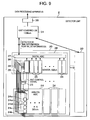
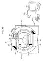
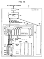
The present invention relates to a nuclear
medicine diagnostic apparatus, and more particularly,
to a positron emission tomography (hereinafter referred
to as "PET") apparatus, which is a kind of a nuclear
medicine diagnostic apparatus using a semiconductor
radiation detector, semiconductor radiation detection
apparatus or detector unit.
A detector using a NaI scintillator is known
as a conventional radiation detector for detecting
radiation such as γ-rays. With a gamma camera (a kind
of nuclear medicine diagnostic apparatus) provided with
a NaI scintillator, radiation (γ-rays) incident on the
scintillator at an angle restricted by many collimators
interacts with NaI crystals and emits scintillation
light. This light travels in such a way as to sandwich
a light guide, reaches a photoelectric multiplier and
becomes an electrical signal. The electrical signal is
shaped by a measuring circuit mounted on a measuring
circuit fixing board and transferred from an output
connector to an external data collection system. All
these scintillator, light guide, photoelectric
multiplier and measuring circuit, measuring circuit
fixing board, etc., are housed in a light shielding
case and shielded from electromagnetic waves other than
external radiation.
Since a gamma camera using a scintillator has
a structure with a large photoelectric multiplier (also
called "photomultiplier") placed after one large
crystal such as NaI, its position resolution remains on
the order of 10 mm. Furthermore, since the scintillator
detects radiation in multi-stages of conversion
from radiation to visible light, from visible light to
electrons, it has a problem of having considerably poor
energy resolution. For example, there is a PET
apparatus (positron emission tomography apparatus)
having position resolution of 5 to 6 mm or a high-end
PET apparatus having position resolution of 4 mm or so,
but since their photoelectric multipliers use vacuum
tubes, it is difficult to further improve position
resolution.
There are radiation detectors for detecting
radiation according to principles different from those
of such a scintillator, such as semiconductor radiation
detectors provided with a semiconductor radiation
detection element using a semiconductor material such
as CdTe (cadmium telluride), TlBr (thallium bromide)
and GaAs (gallium arsenide).
This semiconductor radiation detector is
attracting attention because its semiconductor
radiation detection element converts electrical charge
produced by interaction between radiation and the
semiconductor material to an electrical signal, and
therefore it has better efficiency of conversion to an
electrical signal than the scintillator and can also be
miniaturized.
Meanwhile, when a semiconductor material such
as T1 making up a semiconductor radiation detection
element interacts with radiation in a semiconductor
radiation detector, holes having positive electrical
charge and electrons having negative electrical charge
are generated. While mobility of electrons is
relatively large, mobility of holes is relatively
small. That is, electrons move relatively easily and
holes move with difficulty. This takes more time for
holes to reach an electrode than electrons. Moreover,
holes may be annihilated before reaching the electrode.
This involves a problem that the detection sensitivity
of radiation is worsened. Thus, these problems require
solutions.
It is an object of the present invention to
provide a semiconductor radiation detector capable of
improving detection sensitivity.
SUMMARY OF THE INVENTION
In order to solve the above described
problems, a first embodiment of the present invention
improves detection sensitivity by shortening a distance
between electrodes for charge collection of a
semiconductor radiation detector. That is, the
distance between an anode electrode and cathode
electrode or the thickness of a semiconductor area
sandwiched between the anode electrode and cathode
electrode is 0.2 to 2 mm. In this structure, the
distance from positions of electrons and holes
generated by interaction between the semiconductor
material and radiation to the electrodes is shortened,
and therefore the time required for them to reach the
electrodes is shortened. Furthermore, shortening the
distance up to the electrodes reduces the probability
that holes may be annihilated midway the distance.
A second embodiment of the present invention
is a nuclear medicine diagnostic apparatus comprising a
plurality of unit substrates including a plurality of
semiconductor radiation detectors for introducing
radiation and an integrated circuit for processing
radiation detection signals output from the plurality
of semiconductor radiation detectors. This allows the
semiconductor radiation detectors and the integrated
circuits which process the outputs to be disposed close
to one another, with the result that when weak output
signals of the semiconductor radiation detectors are
transmitted to the integrated circuits, it is possible
to reduce influences of noise on the weak output
signals.
The semiconductor radiation detector, analog
LSI (Large Scale Integrated Circuit), AD converter and
digital LSI are preferably arranged on the unit
substrate in that order and the respective elements are
connected by wiring so that a signal detected by the
semiconductor radiation detector is processed by the
analog LSI, the signal processed by the analog LSI is
processed by the AD converter, and the signal processed
by the AD converter is processed by the digital LSI.
By shortening the distance between the semiconductor
radiation detector and analog LSI in particular, this
structure can shorten the wiring distance between the
semiconductor radiation detector and analog LSI and
thereby reduce noise superimposed on the wiring until
the signal detected by the semiconductor radiation
detector reaches the analog LSI. In an embodiment
which will be described later, the LSI (integrated
circuit) corresponds to an ASIC. Also, the
semiconductor radiation detection apparatus corresponds
to a combined substrate (detector substrate + ASIC
substrate) in the embodiment which will be described
later.
According to the second embodiment, detection
signals when the semiconductor radiation detectors
detect radiation are processed by an application-specific
IC called "ASIC (Application Specific
Integrated Circuit)" and this embodiment is intended to
solve an additional problem discovered by the inventor
et al. that since the detection signals output from the
semiconductor radiation detectors are weak, the ASIC is
easily affected by noise. A reduction of the noise
leads to substantial improvement of detection
sensitivity (count, peak value, time detection
accuracy) by the semiconductor radiation detectors.
Different substrates are preferably used as
the substrate for mounting the semiconductor radiation
detectors and the substrate for mounting the LSI.
During ordinary operation, the two substrates are used
in combination as a combined substrate (unified
substrate) so that in the event of trouble, only the
troubled substrate can be replaced to thereby
facilitate maintenance and examination, etc.
A third embodiment of the present invention
adopts a unit-type construction in which a plurality of
unit substrates including semiconductor radiation
detectors and an integrated circuit are mounted in a
frame in a detachable/attachable manner. Since it is
only necessary to mount a detector unit including a
plurality of unit substrates on a nuclear medicine
diagnostic apparatus, a plurality of semiconductor
radiation detectors can be mounted on the nuclear
medicine diagnostic apparatus at a time. In this way,
the time required to mount the semiconductor radiation
detectors on the nuclear medicine diagnostic apparatus
can be shortened drastically.
The embodiment is preferably adapted so that
these unit substrates can be removed from the detector
unit one by one or the whole detector unit can be
removed from the nuclear medicine diagnostic apparatus,
or more specifically, from the camera, which
facilitates maintenance and examination.
Note that many semiconductor radiation
detectors are used for a nuclear medicine diagnostic
apparatus (radiological diagnostic apparatus) such as
PET, SPECT and gamma camera. For example, a PET uses a
hundred thousand to several hundreds of thousands of
(channels) semiconductor radiation detectors and there
is a demand for shortening the time required to mount
these many semiconductor radiation detectors on the
nuclear medicine diagnostic apparatus. A fourth
embodiment of the present invention is implemented to
meet such a demand. There is also a demand for
facilitating maintenance and examination of
semiconductor radiation detectors.
The present invention can prevent or reduce
deterioration of the detection sensitivity of radiation
using semiconductor radiation detectors. The present
invention can also prevent or reduce deterioration of
signals detected by the semiconductor radiation
detectors. This allows, for example, a nuclear
medicine diagnostic apparatus to obtain clear images.
Other objects, features and advantages of the
invention will become apparent from the following
description of the embodiments of the invention taken
in conjunction with the accompanying drawings.
BRIEF DESCRIPTION OF THE DRAWINGS
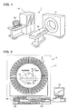
Fig. 1 is a perspective view showing a
structure of a PET apparatus as a nuclear medicine
diagnostic apparatus according to this embodiment;
Fig. 2 schematically shows a cross section in
a circumferential direction of the camera of the PET
apparatus in Fig. 1;
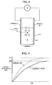
Fig. 3 schematically shows a structure of a
semiconductor radiation detector in a minimum
construction;
Fig. 4 is a graph comparing a "time-peak
value curve" between a case where a thickness t of a
semiconductor material of the semiconductor radiation
detector is large and a case where it is small;
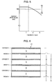
Fig. 5 is a graph schematically showing a
relationship between the thickness t of a semiconductor
material and a peak value (maximum value) of a
semiconductor radiation detector;
Fig. 6 schematically illustrates a
construction of a semiconductor radiation detector
having a laminated structure of semiconductor materials
and electrodes (anodes, cathodes);
Fig. 7A is a front view of a combined
substrate which combines a detector substrate and an
ASIC substrate of the semiconductor radiation detectors
according to this embodiment, Fig. 7B is a side view of
Fig. 7A and Fig. 7C is a perspective view schematically
showing a construction of the semiconductor radiation
detector mounted on the detector substrate in Fig. 7A;
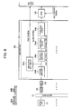
Fig. 8 is a block diagram schematically
showing an analog detection circuit;
Fig. 9 is a block diagram showing a schematic
construction of a digital ASIC and a connection
relationship between an analog ASIC and the digital
ASIC;
Fig. 10 is a perspective view quoted to
illustrate a construction of a detector unit housing a
plurality of semiconductor radiation detectors;
Fig. 11 is a side view of the detector unit
in Fig. 10 without the side plate;
Fig. 12A is a partially exploded perspective
view of a camera when the detector unit is mounted on
the camera and Fig. 12B is a cross-sectional view of
the central part of the camera;
Fig. 13 is a perspective view showing a
construction of a SPECT apparatus as a nuclear medicine
diagnostic apparatus according to another embodiment;
Fig. 14 is a block diagram schematically
showing a circuit construction of an analog ASIC of the
SPECT apparatus in Fig. 13; and
Fig. 15 is a block diagram showing a
schematic construction of a digital ASIC in the SPECT
apparatus in Fig. 13 and a connection relationship
between the analog ASIC and digital ASIC.
DESCRIPTION OF THE EMBODIMENTS
[Embodiment 1]
A nuclear medicine diagnostic apparatus which
is a preferred embodiment of the present invention will
be explained with reference to attached drawings in
detail below as appropriate. The following are
explanations of the nuclear medicine diagnostic
apparatus according to this embodiment, distance
between electrodes of a semiconductor radiation
detector, arrangement (layout) of elements such as
analog ASIC on a substrate, and elements applicable to
this embodiment for construction of substrate units,
etc. Note that an analog ASIC refers to an ASIC
(Application Specific Integrated Circuit) which is an
application-specific IC for processing analog signals
and is a kind of LSI.
«Nuclear medicine diagnostic apparatus»
First, the nuclear medicine diagnostic
apparatus (radiological diagnostic apparatus) according
to this embodiment will be explained. As shown in Fig.
1, a PET apparatus 1 as the nuclear medicine diagnostic
apparatus is constructed by including a camera (image
pickup apparatus) 11, a data processing apparatus 12, a
display apparatus 13, etc. An examinee is laid on a
bed 14 to be photographed using the camera 11. The
camera 11 incorporates many semiconductor radiation
detectors 21 (see Fig. 3, Figs. 7A-7C, Fig. 10) to
detect γ-rays emitted from the body of the examinee
using semiconductor radiation detectors (hereinafter
simply referred to as "detectors") 21. The camera 11
is provided with an integrated circuit (ASIC) for
measuring peak values, detection times of γ-rays and is
designed to measure peak values and detection times of
detected radiations (γ-rays). The data processing
apparatus 12 includes a storage apparatus, a
simultaneous measuring apparatus 12A (see Fig. 2) and a
tomographic information creation apparatus 12B (see
Fig. 2). The data processing apparatus 12 takes in
data of peak values, detection times of detected γ-rays
and packet data including detector (channel) IDs. The
simultaneous measuring apparatus 12A carries out
simultaneous measurements based on this packet data,
especially data of detection times and detector IDs,
identifies detection positions of 511 KeV γ-rays and
stores them in the storage apparatus. The tomographic
information creation apparatus 12B creates a functional
image based on the identified positions and displays it
on the display apparatus 13.
As shown in Fig. 2, inside the camera 11,
many detector units 2 (see Fig. 10 for details) housing
a plurality of combined substrates 20 (see Fig. 7 for
details) provided with many detectors 21 for detecting
γ-rays emitted from the examinee are disposed
circumferentially. The examinee is laid on the bed 14
and positioned at the center of the camera 11. At this
time, the detectors are disposed so as to surround the
bed 14. The detector unit 2 is designed to output for
each detector 21 included in the detector unit 2, peak
value information of γ-rays obtained based on a
detection signal when a detector 21 interact with γ-rays,
time information on γ-ray detection and address
information (detector ID) of each detector 21. The
constructions of the detector 21, combined substrate 20
and detector unit 2 will be explained in detail later.
The examinee is administered radiopharmaceuticals, for
example, fluorodeoxyglucose (FDG) containing 18F whose
half-life is 110 minutes. γ-rays (annihilated γ-rays)
are emitted from the body of the examinee when
positrons emitted from the FDG annihilate.
Hereafter, the characteristic parts of this
embodiment will be explained.
«Semiconductor radiation detector; distance between
electrodes»
First, the detector 21 applied to this
embodiment will be explained. As shown in Fig. 3, the
detector 21 is constructed of a semiconductor radiation
detection element (hereinafter referred to as "detection
element") 211 made of a tabular semiconductor
material S, both sides of which are covered with thin-plate
(film) electrodes (anode A, cathode C) (minimum
construction). Of these components, the semiconductor
material S is made up of a single crystal of any one of
the above described CdTe (cadmium telluride), TlBr
(thallium bromide), GaAs (gallium arsenide), etc.
Furthermore, the electrodes (anode A, cathode C) are
made of any one material of Pt (platinum), Au (gold),
In (indium), etc. In the following explanations,
suppose the semiconductor material S is obtained by
slicing a CdTe single crystal. Furthermore, suppose
radiation to be detected is 511 KeV γ-rays used for the
PET apparatus.
An overview of the principle of γ-ray
detection using the detector 21 will be explained using
Fig. 3. When γ-rays are introduced into the detector 21
and interaction occurs between γ-rays and the
semiconductor material S constituting the detector 21,
an amount of hole and electron pairs schematically
shown in the figure with "+" and "-" corresponding to
the energy of γ-rays is generated. Here, a voltage
(e.g., 300 V) for charge collection is applied between
the electrodes of the anode A and cathode C of the
detector 21. Because of this, holes are moved
attracted to the cathode C and electrons are moved
attracted to the anode A. When holes and electrons are
compared, as described in "Disclosure of the invention"
the ease of movement (mobility) of electrons is
relatively large and therefore electrons reach the
anode in a shorter time. On the other hand, the
mobility of holes is relatively small and therefore
holes take more time to reach the cathode. Note that
holes may be annihilated before reaching the electrode.
As shown in Fig. 4 which shows a comparison
in the "time-peak value curve" between a case where the
semiconductor material S (detection element 211) of the
detector 21 is thick and a case where it is thin, the
semiconductor material S having a smaller thickness t
has a quicker rise of peak value and a higher maximum
value of the peak value. Having a quicker rise of the
peak value contributes to improvement of the accuracy
of simultaneous measurement of the PET, for example.
Furthermore, having a higher peak value contributes to
increasing energy resolution. Thus, a smaller
thickness t speeds up rising of the peak value and
increases the peak value (the efficiency of charge
collection improves) because the time for electrons and
holes to reach the electrodes (anode A, cathode C)
(time of charge collection) is shortened. This is also
because holes which would be conventionally annihilated
midway can reach the electrode (cathode C) without
annihilation because of the shorter distance. Note
that the thickness t can also be expressed by the
distance between the electrodes, anode A and cathode C
facing each other.
The thickness (distance between electrodes) t
of the detection element 211 is preferably 0.2 mm to
2 mm. This is because a thickness t of not less than
2 mm slows down the rising speed of the peak value and
reduces the maximum value of the peak value as well.
On the other hand, a thickness t of smaller than 0.2 mm
relatively increases the thickness (volume) of the
electrodes (anode, cathode) and when installed on a
substrate, the proportion of the very semiconductor
material S that interacts with radiation decreases.
That is, reducing the thickness t of the semiconductor
material S relatively increases the thickness of the
electrode which does not interact with γ-rays on one
hand, and the proportion of the semiconductor material
S which interacts with γ-rays relatively decreases on
the other, with the result that the sensitivity of
detecting γ-rays decreases (γ-rays pass by). Furthermore,
a smaller thickness t may cause more leakage
current preventing a high voltage from being applied
for charge collection.
For the same reason, the thickness t of the
semiconductor material S is preferably 0.5 mm to 1.5 mm
and such a thickness t allows more reliable detection
of γ-rays and more correct measurement of the peak
value, etc.
In the case of the PET apparatus 1, since it
carries out simultaneous measurement, one of problems
to be solved is to correctly measure a γ-ray detection
time. For example, in Fig. 3, there is a difference in
a detection time when positions at which γ-rays interact
with the semiconductor material S are closer to the
cathode C and when those positions are closer to the
anode A. That is, since the moving speed of holes is
lower, the detection time when the interaction occurs
closer to the anode A is relatively late, while the
detection time when the interaction occurs closer to
the cathode C is relatively early (approximates to a
real time). That is, also when γ-rays interact with the
semiconductor material S in the same detection element
211, there is a problem that the detection time changes
depending on the position at which the interaction
takes place. More specifically, when the thickness t
is large, the difference in the detection time
depending on the position at which the interaction
takes place increases. Such an event constitutes no
big problem in other fields, but it constitutes a big
problem in the case of the PET apparatus 1, which
carries out simultaneous measurement (simultaneous
counting) on the order of nsec (nanoseconds).
Therefore, in this sense, too, it is possible to
determine the detection time appropriately within the
above described thickness range. The detection time is
determined by the PET according to an LET system or CFD
system.
As shown in Fig. 5 which schematically shows
a relationship between the thickness t of the
semiconductor material S and peak value (maximum value)
of the detector 21, the maximum value of the peak value
decreases as the thickness t of the semiconductor
material S increases. One of reasons that the peak
value decreases is that holes are annihilated before
reaching the electrode. When the thickness t becomes
2 mm, the peak value of detected radiation falls short
of a threshold whereby it is possible to discriminate
511 KeV γ-rays, and therefore it is not preferable to
increase the thickness t of the semiconductor material
S more than 2 mm as described above.
As shown in Fig. 6, the detector 21 includes
the semiconductor materials S (detection elements 211)
laminated in five layers each sandwiched between the
cathode C and anode A. Each layer of the semiconductor
material S is a single layer detector 21 having the
aforementioned thickness t (0.2 to 2 mm (more
preferably 0.5 to 1.5 mm)). The thickness of the anode
A and cathode C is approximately 20 microns. In the
detector 21 having a laminated structure shown in this
Fig. 6, the different anodes A or different cathodes C
are connected to a common wire, and therefore each
layer is not designed to detect radiation independently
of other layers. In other words, when γ-rays interact
with the semiconductor material S, it is not possible
to discriminate whether the interaction takes place on
the top layer or bottom layer. Of course, it is also
possible to adopt a structure in which radiation is
detected by each layer. This five-layer structure is
adopted because reducing the thickness t of the
semiconductor material S is preferable in increasing
the rising speed of the peak value and increasing the
maximum value of the peak value, but a small thickness
t causes more γ-rays to pass by, and therefore reducing
the amount of γ-rays that pass by while increasing the
efficiency of charge collection increases interaction
between the semiconductor material S and γ-rays (to
increase a count value).
Adopting the detector 21 having such a
laminated structure can obtain a better peak value
rising speed and an accurate peak value and increase
the number of γ-rays (count value)(increase the
sensitivity) that interact with the semiconductor
material S.
An area s of the electrode (anode A, cathode
C) is preferably 4 to 120 mm2. An increase of the area
s increases the capacity (stray capacitance) of the
detector 21 and this increase in the stray capacitance
makes noise easier to superimpose, and therefore the
area s of the electrode is preferably as small as
possible. Furthermore, charge produced when γ-rays are
detected is partially accumulated in the stray
capacitance, and therefore there is a problem that when
the stray capacitance increases, the amount of charge
stored in a charge amplifier 24b of an analog ASIC 24
or further an output voltage (peak value) decreases.
When CdTe is used for the detector 21, its dielectric
constant is 11 and if the area s of the detector 21 is
120 mm2, thickness t is 1 mm, then the capacity is 12
pF, which is not negligible considering the fact that
the stray capacitance of connectors, etc. of the
circuit is several pF. Therefore, the area s of the
electrode is preferably 120 mm2 or less.
Furthermore, the lower limit of the area s of
the electrode is determined by position resolution of
the PET apparatus. The position resolution of the PET
apparatus is determined by not only the size (array
pitch) of the detector 21 but also the positron range,
etc., but since the range of positron of 18F is 2 mm,
setting the size of the detector 21 to 2 mm or less is
meaningless. The method of mounting so that the area
of the electrode becomes a minimum is a case where the
surface of the electrode is placed perpendicular to the
radius direction of the camera 11 and from the above
described consideration, the lower limit of one side of
the electrode is 2 mm and the lower limit of the area s
of the electrode is 4 mm2.
In the above described explanations, CdTe is
used as the semiconductor material S which interacts
with γ-rays, but it goes without saying that the
semiconductor material S may also be TlBr or GaAs, etc.
Moreover, the terms "laminated structure", "upper
layer" and "lower layer" have been used, but these
terms are based on Fig. 6 and when the viewing
direction is turned by 90° toward the horizontal
direction, the laminated structure may be read as a
parallel structure and top/bottom may be read as
right/left, for example. Moreover, the direction of
incident γ-rays may also be upward, downward, rightward
and leftward in Fig. 6. In other words, the detector
21 has a structure in which a plurality of (e.g., five)
semiconductor materials S are arranged in parallel in
such a way as to sandwich cathodes C and anodes A
alternately.
«Combined substrate; detector substrate and ASIC
substrate»
A detailed structure of the combined
substrate (unit substrate) 20 installed in the detector
unit 2 (Fig. 10) will be explained using Figs. 7A-7C.
The combined substrate (semiconductor radiation
detection apparatus) 20 comprises a detector substrate
(first substrate) 20A in which a plurality of detectors
21 are arranged and an ASIC substrate (second
substrate) 20B in which a capacitor 22, a resistor 23,
analog ASICs 24, analog/digital converters (hereinafter
referred to as "ADC") 25 and a digital ASIC 26 are
arranged.
(Detector substrate)
With reference to Figs. 7A-7C, the detector
substrate 20A provided with the detectors 21 will be
explained. As shown in Fig. 7A, the detector substrate
20A has a grid-like arrangement (mounting) of a
plurality of detectors 21 on one side of a substrate
body 20a (4 rows of 16 detectors 21 = horizontal 16 x
vertical 4 = total 64 detectors). In the radius
direction of the camera 11, the detectors 21 are
arranged in four rows on the substrate body 20a. The
16 detectors 21 in the horizontal direction are
arranged in the axial direction of the camera 11, that
is, in the longitudinal direction of the bed 14.
Furthermore, as shown in Fig. 7B, since the
semiconductor radiation detectors 21 are arranged on
both sides of the detector substrate 20A, a total of
128 detectors 21 are arranged on one detector substrate
20A. Here, as the number of detectors 21 to be
installed increases, it is easier to detect γ-rays and
it is possible to increase position accuracy when γ-rays
are detected. For this reason, the detectors 21 are
disposed on the detector substrate 20A as densely as
possible. In Fig. 7A, when γ-rays emitted from the
examinee on the bed 14 travel from bottom to top in the
figure (direction indicated by an arrow 32, that is,
radius direction of the camera 11), arranging the
detectors 21 in the left-to-right direction densely on
the detector substrate 20A is preferable because in
this way, the number of γ-rays that pass by (the number
of γ-rays that pass through the gap between the
detectors 21) is reduced. This increases the detection
efficiency of γ-rays and increases spatial resolution of
an image obtained.
As shown in Fig. 7B, the detector substrate
20A of this embodiment arranges the detectors 21 on
both sides of the substrate body 20a, and therefore the
substrate body 20a can be shared by both sides compared
to the case where the detectors 21 are arranged only on
one side. For this reason, it is possible to reduce
the number of substrate bodies 20a by half and arrange
the detectors 21 more densely in the circumferential
direction. Moreover, as described above, the number of
detector substrates 20A (combined substrates 20) can be
reduced by half, and therefore there is a merit of
saving time and trouble to mount the combined
substrates 20 in the housing 30 (see Fig. 10) which
will be described later.
In the above described explanations, the 16
horizontal detectors 21 are arranged in the axial
direction of the camera 11, but the arrangement is not
limited to this. For example, the 16 horizontal
detectors 21 may also be arranged in the circumferential
direction of the camera 11.
As shown in Fig. 7C, each detector 21 has a
laminated structure of single crystals of the
aforementioned thin-film semiconductor materials S
(detection elements 211). The structure and function
thereof have already been explained with reference to
Fig. 6, but supplementary explanations will be given
here. As described above, the detector 21 is provided
with the anode A and cathode C and a potential
difference (voltage) of, for example, 300 V is applied
between the anode A and cathode C for charge
collection. This voltage is supplied from the ASIC
substrate 20B to the detector substrate 20A via the
connector C1 (Fig. 7A). Furthermore, the signal
detected by each detector 21 is supplied to the ASIC
substrate 20B via the connector C1. Thus, on-board
wiring (for charge collection and signal exchange) (not
shown) for connecting the connector C1 and each
detector 21 is provided in the substrate body 20a of
the detector substrate 20A. This on-board wiring has a
multi-layered structure. In this embodiment, the
detection elements 211 of the detector 21 are arranged
in parallel to the substrate body 20a. However, the
detectors 21 may also be provided so that the
respective detection elements 211 are disposed
perpendicular to the substrate body 20a.
(ASIC substrate)
Then, the ASIC substrate 20B incorporating
the ASIC will be explained. As shown in Fig. 7A, the
ASIC substrate 20B is provided with two analog ASICs 24
and one digital ASIC 26 on one side of the substrate
body 20b. Furthermore, as shown in Fig. 7B, since the
analog ASICs 24 are provided on both sides of the
substrate body 20b, one ASIC substrate 20B includes a
total of four analog ASICs 24. Furthermore, the ASIC
substrate 20B includes eight (=4×2) ADCs 25 on one side
of the substrate body 20b and sixteen ADCs 25 on both
sides. Furthermore, as many capacitors 22 and
resistors 23 as the detectors 21 are arranged on both
sides of one substrate body 20b. Furthermore, to
electrically connect theses capacitors 22, resistors
23, analog ASICs 24, ADCs 25 and digital ASIC 26, the
ASIC substrate 20B (substrate body 20b) is provided
with on-board wiring (not shown) as with the above
described detector substrate 20A. This on-board wiring
also has a laminated structure.
These elements 22, 23, 24, 25 and 26 are
arranged (on-board wiring) so that a signal supplied
from the detector substrate 20A is supplied to the
capacitor 22, resistor 23, analog ASIC 24, ADC 25 and
digital ASIC 26 in that order.
The ASIC substrate 20B includes a connector
(spiral contact) C1 which is connected to the on-board
wiring which is connected to each capacitor 22 to make
electrical connections to the detector substrate 20A
and a substrate connector C2 which makes electrical
connections to the data processing apparatus (the unit
combination FPGA which will be described later). Note
that the above described detector substrate 20A also
includes the connector C1 connected to the on-board
wiring which is connected to each detector 21.
(Connection structure between detector substrate and
ASIC substrate)
The connection structure between the detector
substrate 20A and ASIC substrate 20B will be explained.
The detector substrate 20A and ASIC substrate
20B are connected not with their respective end faces
(ends) facing each other but by providing an overlap
area where both ends overlap with each other and
connecting the connectors C1 in this overlap area as
shown in Fig. 7B. This connection is made in a
detachable/attachable manner using screws for clamping.
These connections are made for the following reason.
That is, when the combined substrate 20 made up of the
detector substrate 20A and ASIC substrate 20B connected
(combined) together is supported on one end (cantilever
support) or on both ends in the horizontal direction, a
force which flexes or bends the combined substrate 20
downward is applied to the central area (connection
area) of the combined substrate 20. Here, in the case
where both ends are the connection area where their
respective end faces (ends) face each other, the
connection area is easily flexed or bent, which is not
preferable.
With consideration given to this aspect, this
embodiment connects the detector substrate 20A and ASIC
substrate 20B not with the respective end faces facing
each other but by providing the overlap area so that
the areas close to the ends overlap with each other as
described above. This improves toughness against
flexure or bending compared to the connection with the
end faces facing each other, which is preferable.
Moreover, improving toughness against flexure or
bending of the combined substrate suppresses
dislocation of the detectors 21 and prevents
deterioration of accuracy of identifying positions at
which γ-rays are generated. As shown in Fig. 2, the
camera 11 of the PET apparatus 1 is provided with many
detector units 2 (Fig. 10) including the combined
substrate 20 shown in Figs. 7A-7C in a doughnut shape
and these combined substrates 20 disposed at positions
of 3 o'clock and 9 o'clock in the horizontal direction
in Fig. 2 are liable to flexure or bending. Thus, the
toughness of the combined substrates 20 against flexure
or bending becomes important.
The detector substrate 20A and ASIC substrate
20B are electrically connected using the aforementioned
overlap area. For this purpose, a connector C1 (Fig.
7A) which electrically connects the on-board wiring of
both the substrates 20A and 20B is provided in the
respective overlap areas of the detector substrate 20A
and ASIC substrate 20B shown in Fig. 7B. For the
connector C1, for example, a spiral contact (R) is used
to improve electrical connections. The spiral
contact(R) is made of a ball-shaped connection terminal
contacting a spiral contactor over a wide area and
provides a characteristic of realizing optimal
electrical connections. Note that when the ball-shaped
connection terminal is provided on the ASIC substrate
20B side, the spiral contactor is provided on the
detector substrate 20A side, and when the ball-shaped
connection terminal is provided on the detector
substrate 20A side, the spiral contactor is provided on
the ASIC substrate 20B side.
Using such an electrical connection structure
between the detector substrate 20A and ASIC substrate
20B allows signals to be sent from the detector
substrate 20A to the ASIC substrate 20B with low loss.
Note that when loss is small, the energy resolution on
the part of the detectors 21 improves.
Furthermore, as described above, the detector
substrate 20A and ASIC substrate 20B are connected in a
freely detachable/attachable manner by means of screws,
etc. Thus, even when trouble occurs in the semiconductor
radiation detectors 21 or ASICs 24, 26, all that
should be done is just to replace the part with
trouble. Therefore, this eliminates waste that the
entire combined substrate 20 must be replaced due to
trouble in that part. Moreover, since electrical
connection between the detector substrate 20A and ASIC
substrate 20B is made by the connector C1 such as the
aforementioned spiral contactor (R), connection or
disconnection (combination or dissociation) between the
substrates can be done easily.
In the above described construction, one
detector substrate 20A is connected to the ASIC
substrate 20B, but it is also possible to divide the
detector substrate into a plurality of portions. For
example, two detector substrates may be connected to
the ASIC substrate, each consisting of eight horizontal
by four vertical detectors 21. According to this
construction, if one detector 21 has trouble, of the
two detector substrates, only the one including the
faulty detector 21 needs to be replaced and it is
therefore possible to reduce waste in maintenance (cost
reduction).
(Element layout)
Then, the layout of elements such as the
detectors 21, ASICs 24, 26 of the combined substrate 20
will be explained with reference to Figs. 7A-7C and
Fig. 8.
As shown in Fig. 8, the detector 21 is
connected to the analog ASIC 24 through the connector
C1, capacitor 22 and resistor 23 by means of electrical
wiring (not shown) and a detection signal of γ-rays
detected by the detector 21 is passed through the
capacitor 22 and resistor 23 by means of the electrical
wiring and processed by the analog ASIC 24.
Furthermore, the signal processed by the analog ASIC 24
is also processed by the ADC 25 and digital ASIC 26.
Here, the shorter the length of the circuit
and length (distance) of the wiring, the better,
because there is less influence of noise or less
attenuation of a signal. Furthermore, when
simultaneous measurement processing is carried out by
the PET apparatus 1, a shorter circuit or wiring is
preferred because its time delay is smaller (preferable
because the accuracy of detection time is not lost).
For this reason, in order of the detector 21, capacitor
22, resistor 23, analog ASIC 24, ADC 25 and digital
ASIC 26 from the center axis of the camera 11 outward
in the radius direction of the camera 11, that is, the
elements 21, 22, 23, 24, 25 and 26 are arranged
(layout) in this embodiment as shown in Fig. 7A. This
order is the same as the signal processing order by the
elements 21, 22, 23, 24, 25 and 26 (see Fig. 8, Fig.
9). That is, from the center axis of the camera 11
outward, the "detector, analog integrated circuit, AD
converter and digital integrated circuit" are arranged
on the substrate in that order and wired in the same
order. Thus, it is possible to transmit a weak signal
detected by the detector 21 to the analog ASIC 24 with
the wiring length (distance) shortened.
Since the signal of the analog ASIC 24 is
subjected to processing such as amplification, it is
less susceptible to influences of noise even if the
length of wiring from the analog ASIC 24 onward is
long. That is, considering noise, there is no problem
even if the wiring length from the analog ASIC 24
onward is long. However, with lengthy wiring, there is
a delay in signal transmission and the accuracy of the
above described detection time may deteriorate.
In this embodiment, since not only the
detector 21 but also the analog ASIC 24 and digital
ASIC 26 are included in one combined substrate 20, the
detector 21, analog ASIC 24 and digital ASIC 26 can be
arranged in the longitudinal direction of the bed 14,
that is, the direction perpendicular to the body axis
of the examinee subject to an examination, and
therefore this eliminates the need to extend the length
of the camera (image pickup apparatus) 11 in the
longitudinal direction of the bed more than necessary.
It is also possible to consider the possibility of
arranging the analog ASIC 24 and digital ASIC 26
outside in the radius direction of the annularly
arranged detector group, and in the longitudinal
direction of the bed 14, but this causes the length of
the camera 11 in the longitudinal direction of the bed
to become longer than necessary. Furthermore,
semiconductor radiation detectors are used as the
detectors 21, and analog ASIC 24 and digital ASIC 26
are used as signal processing apparatuses, the length
of the combined substrate 20 in the longitudinal
direction is shortened and the length of the camera 11
in the orthogonal direction can be shortened
significantly compared to the case where a scintillator
is used. Furthermore, the combined substrate 20 is
provided with the detector 21, analog ASIC 24 and
digital ASIC 26 in that order in the longitudinal
direction thereof, and therefore it is possible to
shorten the length of the wiring connecting them and
simplify the wiring on the substrate.
Here, in this embodiment, one analog ASIC 24
is connected to 32 detectors 21 to process signals
obtained from the detectors 21. As shown in Fig. 8 and
Fig. 9, one analog ASIC 24 is provided with 32 sets of
an analog signal processing circuit (analog signal
processing apparatus) 33 made up of a slow system and
fast system. One analog signal processing circuit 33
is provided for each detector 21 and connected to one
detector 21. Here, the fast system is provided with a
timing pick off circuit 24a to output a timing signal
for identifying a detection time of γ-rays. On the
other hand, the slow system is provided with a polarity
amplifier (linear amplifier) 24c, a band pass filter
(waveform shaping apparatus) 24d and a peak hold
circuit (peak value holding apparatus) 24e connected in
this order for the purpose of calculating a peak value
of the detected γ-rays. Note that the slow system is
named "slow" because it takes a certain degree of
processing time to calculate a peak value. Reference
numeral 24b denotes a charge amplifier (preamplifier).
A γ-ray detection signal output from the detector 21 and
passed through the capacitor 22 and resistor 23 is
amplified at the charge amplifier 24b and polarity
amplifier 24c. The amplified gamma-ray detection
signal is passed through the band pass filter 24d and
input to the peak hold circuit 24e. The peak hold
circuit 24e holds a maximum value of the detection
signal, that is, the peak value of a γ-ray detection
signal proportional to energy of the detected γ-rays.
One analog ASIC 24 is an LSI which integrates 32 sets
of analog signal processing circuits 33.
The capacitor 22 and resistor 23 can also be
provided inside the analog ASIC 24, but this embodiment
arranges the capacitor 22 and resistor 23 outside the
analog ASIC 24 for reasons such as obtaining an
appropriate capacitance and appropriate resistance and
reducing the size of the analog ASIC 24. Note that the
capacitor 22 and resistor 23 are preferably disposed
outside because in this way variations in the
individual capacitance and resistance are reduced.
In the analog ASIC 24 shown in Fig. 8, the
output of the slow system of this analog ASIC 24 in
this embodiment is designed to be supplied to an ADC
(analog/digital converter) 25. Moreover, the output of
the fast system of the analog ASIC 24 is designed to be
supplied to the digital ASIC 26.
The analog ASIC 24 and each ADC 25 are
connected via one wire which sends slow system signals
corresponding to 8 channels all together. Furthermore,
each analog ASIC 24 and digital ASIC 26 are connected
via 32 wires which send 32-channel fast system signals
one by one. That is, one digital ASIC 26 is connected
to four analog ASICs 24 via a total of 128 wires.
The output signal of the slow system output
from the analog ASIC 24 is an analog peak value
(maximum value of the graph shown in Fig. 4).
Furthermore, the output signal of the fast system
output from the analog ASIC 24 to the digital ASIC is a
timing signal showing the timing corresponding to the
detection time. Of these signals, the peak value which
is the slow system output is input to the ADC 25 via
the wire (wire uniting 8 channels into one) connecting
the analog ASIC 24 and ADC 25 and converted to a
digital signal by the ADC 25. The ADC 25 converts a
peak value to, for example, an 8-bit (0 to 255) digital
peak value (e.g., 511 KeV→255). On the other hand, a
timing signal which is a slow system output is supplied
to the digital ASIC 26 via the above described wire
connecting the analog ASIC 24 and digital ASIC 26.
The ADC 25 sends the digitized 8-bit peak
value information to the digital ASIC 26. For this
purpose, each ADC 25 and digital ASIC 26 are connected
via a wire. For example, since there are sixteen ADCs
25 on both sides, the digital ASIC 26 is connected to
the ADC 25 via a total of sixteen wires. One ADC 25
processes signals corresponding to 8 channels (signals
corresponding to eight detection elements). The ADC 25
is connected to the digital ASIC 26 via one wire for
transmission of an ADC control signal and one wire for
transmission of peak value information.
As shown in Fig. 9, the digital ASIC 26
comprises a plurality of packet data generation
apparatuses 34 including eight time decision circuits
(time information generation apparatuses) 35 and one
ADC control circuit (ADC control apparatus) 36, and a
data transfer circuit (data transmission apparatus) 37,
and integrates all these elements into one LSI. All
the digital ASICs 26 provided for the PET apparatus 1
receive a 500 MHz clock signal from a clock generation
apparatus (crystal oscillator) (not shown) and operates
synchronously. The clock signal input to each digital
ASIC 26 is input to the respective time decision
circuits 35 in all the packet data generation
apparatuses 34. One time decision circuit 35 is
provided for each detector 21 and receives a timing
signal from the timing pick off circuit 24a of the
corresponding analog signal processing circuit 33. The
time decision circuit 35 determines the detection time
of γ-rays based on the clock signal when the timing
signal is input. Since the timing signal is based on
the fast system signal of the analog ASIC 24, a time
close to a real detection time can be set as the
detection time (time information). The ADC control
circuit 36 receives a timing signal for the timing at
which γ-rays are detected from the time decision circuit
35 and identifies the detector ID. That is, the ADC
control circuit 36 stores a detector ID corresponding
to each time decision circuit 35 connected to the ADC
control circuit 36 and can identify, when time
information is input from a certain time decision
circuit 35, the detector ID corresponding to the time
decision circuit 35. This is possible because one time
decision circuit 35 is provided for each detector 21.
Moreover, after inputting the time information, the ADC
control circuit 36 outputs an ADC control signal
including detector ID information to the ADC 25. The
ADC 25 outputs the peak value information output from
the peak hold circuit 24e of the analog signal
processing circuit 33 corresponding to the detector ID
by converting it to a digital signal. This peak value
information is input to the ADC control circuit 36.
The ADC control circuit 36 adds the peak value
information to the time information and detector ID to
create packet data. The ADC control circuit 36 has the
functions of the ADC control apparatus for controlling
the ADC 25 and the information combination apparatus
for combining the detector ID information (detector
position information), time information and peak value
information. The information combination apparatus
outputs combination information (packet information)
which is digital information including those three
kinds of information. The packet data (including
detector ID, time information and peak value
information) output from the ADC control circuit 36 of
each packet data generation apparatus 34 is input to
the data transfer circuit 38.
The data transfer circuit 38 sends packet
data which is digital information output from the ADC
control circuit 36 of each packet data generation
apparatus 34 to the integrated circuit (unit
combination FPGA (Field Programmable Gate array)) 31
for unit combination provided for the housing 30 of the
detector unit 2 (Fig. 10, Fig. 11) which houses twelve
combined substrates 20, for example, periodically. The
unit combination FPGA (hereinafter referred to as
"FPGA") 31 sends the digital information to the data
processing apparatus 12 through an information
transmission wire connected to the connector 38.
Since the ADC 25 converts the peak value
information output from the peak hold circuit 24e
corresponding to the detector ID information included
in a control signal output from the ADC control circuit
36 to a digital signal, one ADC 25 is provided for a
plurality of analog signal processing circuits 33 in
one analog ASIC 24. Therefore, there is no need to
provide one ADC 25 for each of a plurality of analog
signal processing circuits 33 and it is possible to
thereby significantly simplify the circuit construction
of the ASIC substrate 20B. Also one information
combination apparatus for generating combination
information is enough for a plurality of analog signal
processing circuits 33 in one analog ASIC 24, which can
simplify the circuit construction of the digital ASIC
26. Moreover, only one ADC control apparatus for
identifying detector IDs needs to be provided for a
plurality of analog signal processing circuits 33 in
one analog ASIC 24, simplifying the circuit
construction of the digital ASIC 26.
In this way, packet data output from the
digital ASIC 26 and including detector IDs for uniquely
identifying (1) peak value information, (2) determined
time information and (3) detector 21, one by one is
sent to the next data processing apparatus 12 (see Fig.
1) through an information transmission wire. The
simultaneous measuring apparatus 12A of the data
processing apparatus 12 carries out simultaneous
measuring processing (when two γ-rays with predetermined
energy are detected with a time window with a set time,
this processing regards these γ-rays as a pair of γ-rays
generated by annihilation of one positron) based on the
packet data sent from the digital ASIC 26, counts the
simultaneously measured pair of γ-rays as one γ-ray and
identifies the positions of the two detectors 21 which
have detected the pair of γ-rays using those detector
IDs. When there are three or more γ-rays detection
signals detected within the above described time window
(when there are three or more detected detectors 21
which have detected γ-rays) the data processing
apparatus 12 identifies the two detectors 21 into which
γ-rays are introduced first out of three or more
detectors 21 using peak value information, etc., on
those γ-ray detection signals. The identified one pair
of detectors 21 are simultaneously measured and one
count value is generated. Furthermore, the tomographic
information creation apparatus 12B of the data
processing apparatus 12 creates tomographic information
on the examinee at the position where radiopharmaceuticals
are concentrated, that is, position of malignant
tumor, using count values obtained by simultaneous
measurement and position information on the detectors
21. This tomographic information is displayed on the
display apparatus 13. Information such as the above
described digital information, count value obtained by
simultaneous measurement and position information on
the detectors 21 and tomographic information are stored
in the storage apparatus of the data processing
apparatus 12.
According to the above described
explanations, the detector substrate 20A includes the
detectors 21 and the ASIC substrate 20B includes the
capacitor 22, resistor 23, analog ASIC 24, ADC 25 and
digital ASIC 26. However, the detector substrate
(first substrate) 20A may include the detector 21,
capacitor 22, resistor 23 and analog ASIC 24, etc., and
the ASIC substrate (second substrate) 20B may include
the ADC 25 and digital ASIC 26, etc. By the detector
substrate 20A including the detectors 21 and analog
ASIC 24, the distance (wire length) between the
detector 21 and analog ASIC 24 can be further
shortened. Thus, it is possible to further reduce
influences of noise.
Furthermore, the combined substrate 20 may
include three substrates (detector substrate 20A,
analog ASIC substrate and digital ASIC substrate) and
they may be connected in a detachable/attachable manner
through their respective connectors.
In this case, of the three substrates, the
detector substrate 20A includes the detectors 21, the
analog ASIC substrate includes the capacitor 22,
resistor 23 and analog ASIC 24 and the digital ASIC
substrate includes the ADC 25 and digital ASIC 26.
This structure separates the substrate incorporating
the analog circuit from the substrate incorporating the
digital circuit to thereby prevent noise on the digital
circuit side from entering the analog circuit.
Furthermore, this structure separates the substrate
incorporating the analog ASIC from the substrate
incorporating the digital ASIC and connects the two
substrates using a detachable/attachable connector, and
therefore even when only the digital ASIC malfunctions,
only the digital ASIC substrate needs to be replaced.
In this way, this structure can further reduce waste.
In the above explanations, the substrate body
20a (detector substrate 20A) for mounting the detectors
21 is different from the substrate body 20b (ASIC
substrate 20B) for mounting the ASICs 24, 26. Thus,
when, for example, both ASICs are soldered to a
substrate by means of a BGA (Ball Grid Array) using
reflow, only the ASIC substrate can be soldered and
this is preferable because the semiconductor radiation
detector 21 need not be exposed to a high temperature.
Of course, it is also possible to arrange all the
elements 21 to 26 on the same substrate and use no
connector C1.
«Detector unit; unit construction through housing of
combined substrate»
Next, a unit construction by housing the
above described combined substrate 20 in the housing 30
will be explained. This embodiment constructs a
detector unit (twelve substrate units) 2 by housing
twelve combined substrates 20 in the housing (frame)
30. The camera 11 of the PET apparatus 1 has a
structure in which 60 to 70 detector units 2 are
arranged in the circumferential direction in a
detachable/attachable manner (see Fig. 12B) so as to
facilitate maintenance and examination (see Fig. 2).
(Housing in housing)
As shown in Fig. 10, the detector unit 2 is
provided with a housing 30, etc., for housing or
holding the above described 12 combined substrates 20,
a high-voltage power supply PS for supplying a charge
collecting voltage to these 12 combined substrates 20,
the above described FPGA 31, signal connectors for
exchanging signals with the outside and power
connectors for receiving a power supply from the
outside.
As shown in Fig. 10 and Fig. 11, the combined
substrates 20 are housed in the housing 30, arranged in
three rows in the depth direction (longitudinal
direction of the bed 14) without overlapping with one
another and in four rows in the width direction
(circumferential direction of the camera 11). Namely,
one housing 30 houses twelve combined substrates 20.
To realize such housing, a guide member 39 consisting
of four rows of guide grooves (guide rails) G1
extending in the depth direction and arranged at
appropriate intervals in the circumferential direction
is disposed in the housing 30 and fitted at the upper
end of the housing (cover) 30. The guide member 39 has
an opening 40 opposed to each connector C3 of a ceiling
plate 30a in the portion of each guide groove G1.
Furthermore, a bottom plate 30b of the housing 30 is
provided with four guide members 41 having one guide
groove (guide rail) G2 extending in the depth direction
arranged at appropriate intervals in the circumferential
direction (see Fig. 11). The guide grooves G1, G2
have a depth corresponding to a capacity of housing
three combined substrates 20. An end of the combined
substrate 20 on the ASIC substrate 20B side is housed
in the guide groove G1 and an end of the combined
substrate 20 on the detector substrate 20A side is
housed in the guide groove G2. Three combined
substrates 20 are held in the depth direction of the
guide grooves G1, G2. Note that since the end of the
combined substrate 20 on the ASIC substrate 20B side
and the other end on the detector substrate 20A side
are designed to be slidable in the guide grooves G1,
G2, it is possible to easily position the combined
substrates 20 at predetermined locations by sliding
them in the guide grooves G1, G2 with fingers, for
example. In this case, each substrate connector C2 is
positioned in the portion of each opening 40. After a
predetermined number of combined substrates 20 are
arranged in the housing 30, the ceiling plate 30a is
attached at the top end of the housing 30 in a
detachable/attachable manner using screws, etc. Each
connector C3 fitted in the ceiling plate 30a is
inserted in the corresponding opening 40 and connected
to the corresponding substrate connector C2. The terms
"upper" and "lower" sections of the housing 30 are
applicable when the housing 30 is removed from the
camera 11, and when the housing 30 is mounted in the
camera 11 as shown in Fig. 2, the upper and lower
sections may be inverted or turned 90 degrees to be
"right" and "left" sections or located diagonally.
As shown in Fig. 11, the ceiling plate 30a of
the housing 30 is provided with not only the four rows
of guide grooves G1 but also FPGA 31 and connector 38.
The connector 38 is connected to the FPGA 31. The FPGA
31 is programmable in the field. In this aspect, the
FPGA 31 is different from the ASIC in that it is not
programmable. Therefore, as with this embodiment, even
if the number or type of the combined substrates 20 to
be housed changes, the FPGA 31 can be programmed in the
field to be adaptable to changes in the number of
substrates appropriately.
Since the detectors 21 using CdTe as the
semiconductor material S in this embodiment generate
charge in reaction with light, the housing 30 is made
of a material having light shielding properties such as
aluminum and an alloy of aluminum and designed in such
a way as to eliminate gaps through which light enter.
That is, the housing 30 is constructed to secure light
shielding properties. If, for example, light shielding
properties are secured by other means, the housing 30
itself need not be provided with light shielding
properties and the housing 30 can be a frame
(framework) to hold the detectors 21 in a detachable/attachable
manner (e.g., no light shielding plane
member (panel), etc., is required).
As shown in Fig. 12A, the detector unit 2 is
mounted via a unit support member 2A. Furthermore, as
shown in Fig. 12B, the detector unit 2 is mounted in
the camera 11 with one end supported by the unit
support member 2A. The unit support member 2A has a
hollow disk (doughnut) shape and is provided with many
windows (as many as the detector units 2 to be mounted)
in the circumferential direction of the camera 11. In
order to support the detector units 2 at one end, a
flange portion serving as a stopper is provided on the
front side in the axial direction of the body of the
housing 30 of the detector unit 2. Note that the
flange portions inside in the circumferential direction
become obtrusive when the detector units 2 are arranged
as dense as possible in the circumferential direction.
Therefore, it is possible to remove the obtrusive
flange portions from the housing 30 and allow the
flange portions outside in the circumferential
direction to remain. Or it is also possible to provide
another unit support member 2A and support both ends of
the detector unit 2 by the two unit support members 2A.
In order to mount the detector units 2 in the
unit support member 2A, this embodiment allows many
detectors 21 to be mounted in the camera 11 at a time.
This can considerably shorten the time of mounting the
detectors 21 in the camera 11. Furthermore, packet
data (all packet data for all detectors 21 of a
combined substrate 20) output from the data transfer
apparatus 38 of all the combined substrates 20 in the
detection unit 2 is sent from the unit combination FPGA
31 provided in the detection unit 2 to the data
processing apparatus 12. In this way, the number of
wires through which packet data is transmitted to the
data processing apparatus 12 in this embodiment is also
significantly reduced compared to the case where packet
data is sent from each data transfer apparatus 38 of
the combined substrate 20 to the data processing
apparatus 12.
When the detector units 2 is mounted in the
camera 11, a cover 11a is removed to make the unit
support member 2A exposed so that the detector units 2
are inserted until the detector units 2 touch the
flange portions. When the detector units 2 are
inserted and fitted, connections between the camera 11
and the detector units 2 are made, and signals and
power supply are connected between the camera 11 and
the detector units 2.
(Power supply)
Then, the high-voltage power supply apparatus
PS for supplying a charge collection voltage will be
explained. As shown in Fig. 10, the detector unit 2
provides the high-voltage power supply apparatus PS for
supplying a charge collection voltage to each detector
21 in a space formed inside the housing 30 on the back
of the FPGA 31. This high-voltage power supply
apparatus PS receives a low voltage power supply,
boosts the voltage to 300 V using a DC-DC converter
(means for boosting the voltage, which is not shown)
and supplies the voltage to each detector 21. 64
detectors 21 are provided per one combined substrate 20
(= detector substrate 20A) on one side, and 128 on both
sides. Twelve such combined substrates 20 are housed
in one housing 30 (that is, one detector unit 2).
Thus, the high-voltage power supply apparatus PS
supplies voltages to 128x12=1536 detectors 21.
Conventionally, a supply voltage of 300 V
with extremely small fluctuations is supplied from a
precision power supply apparatus in a remote place, but
since (1) when the distance from the precision power
supply apparatus increases, a wider insulating
structure for high voltage wiring is required (the
insulating distance increases) and (2) the voltage
fluctuates due to a temperature variation of the
detectors 21, there is a problem that supplying a
precise voltage from the precision power supply
apparatus does not necessarily result in a precise
voltage in the part of the target detectors 21.
Furthermore, to facilitate maintenance and
examination, it is also possible to consider providing
the detector unit 2 according to this embodiment with a
power connector (not shown) and removing a high-voltage
power line extending from the precision power supply
apparatus at this power connector. That is, according
to this embodiment, it is possible to consider
supplying a high-voltage power supply to the detector
units 2 from outside the units 2 via power connectors.
However, in the case of a high voltage of 300 V, this
results in a problem that the size of the power
connector increases in addition to the above described
problem of insulation.
According to this embodiment, the high-voltage
power supply apparatus PS built in the detector
unit 2 is connected to an external low voltage (5 to 15
V) DC power supply through the power connector 42 and
connector 38 provided on the ceiling plate 30a via
power wiring. A high-voltage terminal of the high-voltage
power supply apparatus PS is connected to
twelve connectors C3 provided on the ceiling plate 30a
through the connector 43 provided on the ceiling plate
30a and connected to electrodes C of the respective
detectors 21 provided on the substrate body 20a through
the connector C2 of the respective combined substrates
20, power wiring (not shown) in the substrate body 20b,
connector C1 and power wiring (not shown) in the
substrate body 20a. The connectors C1, C2 include not
only connectors for transmitting output signals of the
detectors 21 but also connectors for power wiring.
Since the high-voltage power supply apparatus PS boosts
a low voltage applied from the power supply to 300 V
using a DC-DC converter, it is possible to reduce the
high-voltage section and thereby shorten the insulation
distance. That is, this eliminates the necessity for
using high-voltage wiring for a portion from the
connector 42 to the DC power supply. It also
facilitates maintenance, etc. For the problem with
voltage fluctuations, this embodiment provides not the
high-precision power supply apparatus but the high-voltage
power supply apparatus PS having accuracy
according to a temperature fluctuation of the voltage.
This eliminates the necessity for a high-precision
power supply. Furthermore, since it is a low voltage
that is received from an external power supply, it is
possible to use a small power connector to be provided
for the connector 38. Using the small power connector
increases the degree of freedom in the layout.
Furthermore, since the high-voltage power supply
apparatus PS is arranged in a space formed in the
housing 30 on the back side of the FPGA 31, the
arrangement of the high-voltage power supply apparatus
PS in the housing 30 makes the detector unit 2 more
compact instead of upsizing. It is also possible to
directly connect the high-voltage power supply
apparatus PS to the power wiring provided on the
substrate body 20a through the connector, without the
ceiling plate 30a. Furthermore, the power connector
can also be separated from the output signal connector
of the detector 21. This prevents noise from entering
the signal wiring from the power supply system.
Furthermore, by reducing a supply voltage to
the detector unit 2, it is possible to supply power to
the high-voltage power supply apparatus PS at a low
voltage through the unit combination FPGA 31 as with
power supplies to the ASICs 24, 26.
Furthermore, supplying power using the high-voltage
power supply apparatus PS eliminates the
necessity for insulation from the housing (GND).
The voltage supplied from the FPGA 31 to the
high-voltage power supply apparatus PS is boosted to
300 V by a DC-DC converter (not shown) in the high-voltage
power supply apparatus PS and after boosting,
passed through the ceiling plate 30a of the housing 30
and supplied from ASIC substrate 20B→detector substrate
20A→each detector 21 for each combined substrate 20.
That is, the housing 30 (ceiling plate 30a) is provided
with wiring for voltage supply (not shown) for
supplying a voltage from the high-voltage power supply
apparatus PS to each combined substrate 20.
Furthermore, each combined substrate 20 is provided
with wiring for voltage supply which supplies a voltage
supplied from the high-voltage power supply apparatus
PS to each detector 21 via the substrate connector C2.
[Embodiment 2]
A nuclear medicine diagnostic apparatus
according to another embodiment will be explained. The
nuclear medicine diagnostic apparatus of this embodiment
is single photon emission computer tomography
(SPECT) apparatus.
This SPECT apparatus 51 will be explained
using Figs. 13 to 15. The SPECT apparatus 51 is
provided with a pair of radiation detection blocks 52,
a rotary holder (body of rotation) 57, a data
processing apparatus 12A and a display apparatus 13.
The radiation detection blocks 52 are disposed at two
positions with a 180° difference in the circumferential
direction of the rotary holder 57. More specifically,
the respective unit support members 56 of the radiation
detection blocks 52 are mounted on the rotary holder 57
with a 180° difference in the circumferential direction.
A plurality of detector units 2A each including twelve
combined substrates 53 are mounted on the respective
unit support members 56 in a detachable/attachable
manner. Thus, the detectors 21 are supported by the
unit support member. The construction of each detector
unit 2A is the same as that of the detector unit 2
according to Embodiment 1 except the construction of
the combined substrate 53.
The combined substrate 53 includes a detector
substrate 20A and an ASIC substrate 53B as with the
above described combined substrate 20 (Fig. 14). The
detectors 21 at one end of each detector substrate 20A
are arranged facing the bed 14. A collimator 55 made
of a radiation shielding member (e.g., lead, tungsten,
etc.) is provided on each radiation detection block 52.
Each collimator 55 forms many radiation passages
through which radiation (e.g., γ-rays) passes. These
radiation passages are provided in a one-to-one
correspondence with the detectors 21 positioned at one
end of all the detector substrates 20A of one radiation
detection block 52. All the combined substrates 53 and
collimators 55 are arranged within a light/electromagnetic
shield 54 mounted on the rotary holder 57.
The collimator 55 is mounted in the light/electromagnetic
shield 54. The light/electromagnetic shield
54 cuts off influences of electromagnetic waves other
than γ-rays on the detectors 21, etc.
When the bed 14 on which an examinee
administered with radiopharmaceuticals is laid is
moved, the examinee is moved between the pair of
radiation detection blocks 52. When the rotary holder
57 is rotated, the detector units 2A of each radiation
detection block 52 revolve around the examinee. γ-rays
emitted form an area in the body of the examinee where
radiopharmaceuticals are concentrated (e.g., affected
area) C pass through the radiation passages of the
collimator 55 and are introduced into the corresponding
detectors 21. The detectors 21 output γ-rays detection
signals. These γ-ray detection signals are processed by
analog ASIC 24A and digital ASIC 26A, which will be
described later.
The construction of the detector substrate
20A used in this embodiment (Embodiment 2) is the same
as that in Embodiment 1 and therefore the explanations
will be omitted in this embodiment. The ASIC substrate
53B making up the combined substrate 53 will be
explained using Figs. 14 and 15. As with the combined
substrate 20, the ASIC substrate 53B connected to the
detector substrate 20A through the connector C1
includes a capacitor 22 and a resistor 23, four analog
ASICs 24A and one digital ASIC 26A for each detector
21.
One analog ASIC 24A is provided with 32 sets
of analog signal processing circuits (analog signal
processing apparatuses) 33A having a slow system and
fast system. One analog signal processing circuit 33A
is provided for each detector 21. Here, the fast
system includes a trigger output circuit 24f which
outputs a trigger signal for specifying detection of γ-rays.
As with the analog ASIC 24, the slow system is
provided with a charge amplifier 24b, a polarity
amplifier 24c, a band pass filter 24d and a peak hold
circuit 24e connected in this order. One analog ASIC
24A integrates 32 sets of analog signal processing
circuits 33A into one LSI. A γ-ray detection signal
which is output from the detector 21 and has passed
through the capacitor 22 and resistor 23 are guided
through the charge amplifier 24b, polarity amplifier
24c and band pass filter 24d and input to the peak hold
circuit 24e. The peak hold circuit 24e holds a peak
value of the γ-ray detection signal. The γ-ray
detection signal output from the band pass filter 24d
is input to the trigger output circuit 24f. The
trigger output circuit 24f outputs a trigger signal
when a γ-ray detection signal at a set level or higher
is input to remove influences of noise.
The digital ASIC 26A includes a packet data
generation apparatus 34A and a data transfer circuit 37
and integrates them into one LSI. The above described
trigger signal is input to the ADC control circuit 36A
of the packet data generation apparatus 34A. All the
digital ASICs 26A provided on the SPECT apparatus 51
receive a 64 MHz clock signal from a clock generation
apparatus (crystal oscillator) (not shown) and operate
synchronously. The clock signal input to each digital
ASIC 26A is input to the respective ADC control
circuits 36A in all the packet data generation
apparatuses 34A. The ADC control circuit 36A
identifies the detector ID when the trigger signal is
input. That is, the ADC control circuit 36A stores a
detector ID for each trigger output circuit 24f
connected to the ADC control circuit 36A and can
identify, when a trigger signal is input from a certain
trigger output circuit 24f, the detector ID
corresponding to the trigger output circuit 24f. The
ADC control circuit 36A outputs an ADC control signal
including the detector ID information to the ADC 25.
The ADC 25 converts the peak value information output
from the peak hold circuit 24e of the analog signal
processing circuit 33A corresponding to the detector ID
to a digital signal and outputs it. This peak value
information is input to the ADC control circuit 36.
The ADC control circuit 36A adds the peak value
information to the detector ID to generate packet data.
The packet data (including detector ID and peak value
information) which is the digital information output
from the ADC control circuit 36A of each packet data
generation apparatus 34A is input to the data transfer
circuit 37. The data transfer circuit 37 sends the
packet data output from each ADC control circuit 36A to
the unit combination FPGA 31 of the detector unit 2A
periodically. The unit combination FPGA 31 outputs the
digital information to the information transmission
wiring connected to the connector 38.
Packet data output from the unit combination
FPGA 31 is sent to the data processing apparatus 12A.
A rotation angle detected by an angle gauge (not shown)
connected to the rotation shaft of a motor (not shown)
for rotating the rotary holder 57 is input to the data
processing apparatus 12A. This rotation angle
indicates the rotation angle of each radiation
detection block 52 and more specifically indicates the
rotation angle of each detector 21. Based on this
rotation angle, the data processing apparatus 12A
determines the position (position coordinates) of each
revolving detector 21 on the revolving orbit. In this
way, the position (position coordinates) of the
detector 21 when γ-rays are detected is calculated.
Based on the calculated position of the detector 21,
the data processing apparatus 12A counts γ-rays whose
peak value information reaches and exceeds a set value.
This counting is performed on each area obtained by
dividing the revolving circle into 0.5° portions
relative to the rotational center of the rotary holder
57. The peak value information is an accumulated value
of peak values of respective γ-ray detection signals of
a plurality of detectors 21 (four detectors 21 arranged
on a straight line in Fig. 7A) positioned on an
extension of the radiation passage of the collimator
55. Using the position information of the detectors 21
and count value (count information) of γ-rays when γ-rays
are detected, the data processing apparatus 12A
creates tomographic information on a position at which
radiopharmaceuticals are concentrated, that is,
position of malignant tumor of the examinee. This
tomographic information is displayed on the display
apparatus 13. Information such as the above described
packet information, count value obtained by
simultaneous measurement, position information of the
detector 21 and tomographic information are stored in
the storage apparatus of the data processing apparatus
12.
The foregoing embodiments have described the
PET apparatus 1 and SPECT apparatus 51, but the present
invention is also applicable to a γ camera. Functional
images obtained from the γ camera are two-dimensional
and the γ camera is provided with a collimator for
regulating angles of incidence of γ-rays. Moreover, it
is also possible to adopt a construction of a nuclear
medicine diagnostic apparatus combining the PET
apparatus 1 and SPECT apparatus 51, and an X-ray CT.
Mounting (housing) of the detector unit 2 in
the camera 11 is not limited to the mounting using the
above described unit support member 2A, but any
mounting/housing means or method can be used.
It should be further understood by those
skilled in the art that although the foregoing
description has been made on embodiments of the
invention, the invention is not limited thereto and
various changes and modifications may be made without
departing from the spirit of the invention and the
scope of the appended claims.