EP1520449B1 - Power supply unit for light-emitting diodes - Google Patents
Power supply unit for light-emitting diodes Download PDFInfo
- Publication number
- EP1520449B1 EP1520449B1 EP03762563A EP03762563A EP1520449B1 EP 1520449 B1 EP1520449 B1 EP 1520449B1 EP 03762563 A EP03762563 A EP 03762563A EP 03762563 A EP03762563 A EP 03762563A EP 1520449 B1 EP1520449 B1 EP 1520449B1
- Authority
- EP
- European Patent Office
- Prior art keywords
- emitting diodes
- power supply
- light emitting
- current
- diode
- Prior art date
- Legal status (The legal status is an assumption and is not a legal conclusion. Google has not performed a legal analysis and makes no representation as to the accuracy of the status listed.)
- Expired - Lifetime
Links
Images
Classifications
-
- H—ELECTRICITY
- H05—ELECTRIC TECHNIQUES NOT OTHERWISE PROVIDED FOR
- H05B—ELECTRIC HEATING; ELECTRIC LIGHT SOURCES NOT OTHERWISE PROVIDED FOR; CIRCUIT ARRANGEMENTS FOR ELECTRIC LIGHT SOURCES, IN GENERAL
- H05B45/00—Circuit arrangements for operating light-emitting diodes [LED]
- H05B45/10—Controlling the intensity of the light
- H05B45/14—Controlling the intensity of the light using electrical feedback from LEDs or from LED modules
-
- H—ELECTRICITY
- H05—ELECTRIC TECHNIQUES NOT OTHERWISE PROVIDED FOR
- H05B—ELECTRIC HEATING; ELECTRIC LIGHT SOURCES NOT OTHERWISE PROVIDED FOR; CIRCUIT ARRANGEMENTS FOR ELECTRIC LIGHT SOURCES, IN GENERAL
- H05B45/00—Circuit arrangements for operating light-emitting diodes [LED]
- H05B45/30—Driver circuits
- H05B45/36—Circuits for reducing or suppressing harmonics, ripples or electromagnetic interferences [EMI]
-
- H—ELECTRICITY
- H05—ELECTRIC TECHNIQUES NOT OTHERWISE PROVIDED FOR
- H05B—ELECTRIC HEATING; ELECTRIC LIGHT SOURCES NOT OTHERWISE PROVIDED FOR; CIRCUIT ARRANGEMENTS FOR ELECTRIC LIGHT SOURCES, IN GENERAL
- H05B45/00—Circuit arrangements for operating light-emitting diodes [LED]
- H05B45/30—Driver circuits
- H05B45/37—Converter circuits
- H05B45/3725—Switched mode power supply [SMPS]
-
- H—ELECTRICITY
- H05—ELECTRIC TECHNIQUES NOT OTHERWISE PROVIDED FOR
- H05B—ELECTRIC HEATING; ELECTRIC LIGHT SOURCES NOT OTHERWISE PROVIDED FOR; CIRCUIT ARRANGEMENTS FOR ELECTRIC LIGHT SOURCES, IN GENERAL
- H05B45/00—Circuit arrangements for operating light-emitting diodes [LED]
- H05B45/30—Driver circuits
- H05B45/395—Linear regulators
-
- F—MECHANICAL ENGINEERING; LIGHTING; HEATING; WEAPONS; BLASTING
- F21—LIGHTING
- F21V—FUNCTIONAL FEATURES OR DETAILS OF LIGHTING DEVICES OR SYSTEMS THEREOF; STRUCTURAL COMBINATIONS OF LIGHTING DEVICES WITH OTHER ARTICLES, NOT OTHERWISE PROVIDED FOR
- F21V31/00—Gas-tight or water-tight arrangements
- F21V31/04—Provision of filling media
-
- F—MECHANICAL ENGINEERING; LIGHTING; HEATING; WEAPONS; BLASTING
- F21—LIGHTING
- F21Y—INDEXING SCHEME ASSOCIATED WITH SUBCLASSES F21K, F21L, F21S and F21V, RELATING TO THE FORM OR THE KIND OF THE LIGHT SOURCES OR OF THE COLOUR OF THE LIGHT EMITTED
- F21Y2115/00—Light-generating elements of semiconductor light sources
- F21Y2115/10—Light-emitting diodes [LED]
-
- Y—GENERAL TAGGING OF NEW TECHNOLOGICAL DEVELOPMENTS; GENERAL TAGGING OF CROSS-SECTIONAL TECHNOLOGIES SPANNING OVER SEVERAL SECTIONS OF THE IPC; TECHNICAL SUBJECTS COVERED BY FORMER USPC CROSS-REFERENCE ART COLLECTIONS [XRACs] AND DIGESTS
- Y02—TECHNOLOGIES OR APPLICATIONS FOR MITIGATION OR ADAPTATION AGAINST CLIMATE CHANGE
- Y02B—CLIMATE CHANGE MITIGATION TECHNOLOGIES RELATED TO BUILDINGS, e.g. HOUSING, HOUSE APPLIANCES OR RELATED END-USER APPLICATIONS
- Y02B20/00—Energy efficient lighting technologies, e.g. halogen lamps or gas discharge lamps
- Y02B20/30—Semiconductor lamps, e.g. solid state lamps [SSL] light emitting diodes [LED] or organic LED [OLED]
Definitions
- the present invention relates to a power supply for LEDs.
- a transducer principle is used which generates a periodically fluctuating by a DC value, triangular alternating current through the light emitting diodes.
- LEDs Light-emitting diodes
- LEDs have long since gained their place in many fields where there is a need for low-power optical display systems or lighting systems, e.g. in traffic and signaling technology.
- the raw LED chip with the structure and the terminals is mounted face-up with conductive adhesive on the circuit board.
- This process is referred to in Anglo-American usage as "the bonding".
- the bonding After curing of the adhesive takes place in an additional step connecting the chip terminals to the circuit board using a known from the production of integrated circuits wire bonder.
- the individual chip connections and the circuit board are connected with a gold wire.
- special printed circuit board materials excellent thermal conduction properties can be achieved. This results in a longer life and a higher light output per area.
- the LED array is protected from mechanical damage by shock or vibration.
- Special printed circuit boards with reflector layers serve for light bundling and increasing the light intensities at smaller radiation angles.
- LED modules can thus by using light emitting diodes, which are applied by means of COB technology as LED arrays on a circuit board, efficient lighting units high luminous efficacy, long life, space-saving design and a relatively low cost can be produced. Due to the achievable luminous flux values, these modules are not just signal and Rear lighting interesting, but can be used directly as a means of lighting. COB-technology LED arrays with a 180 ° beam angle allow for bright illumination of surfaces with a homogeneous light distribution comparable to the illumination of a 40 to 50 mA fluorescent lighting system. Another advantage is the 50% lower power consumption compared to such a lighting system.
- Point light sources made of high-performance light-emitting diodes in COB technology are ideal for small work and reading lights, as flexibly usable light sources in spotlights, as a central light source for orientation lights, etc.
- EP 948241 A2 discloses a circuit for controlling LEDs by means of a converter, wherein a storage inductor, LEDs and a switching element are connected in series.
- the circuit has a freewheeling current path, which is connected in parallel with the storage inductor and the LEDs.
- the disclosed circuit for controlling the LEDs makes it possible to ensure a reliable power supply of the LEDs.
- a charge as well as a discharge current of the storage inductor can flow through the LEDs.
- the circuit also makes it possible to measure a zero crossing of the discharge current of the storage inductor, in which a switching of the switching element takes place.
- the thus enabled control of the current profile has a large current deviation between the maximum value and the zero value, which can be disadvantageous for the power supply of an LED.
- the present invention is intended to provide a power supply for light-emitting diodes, which can be easily adapted to different LEDs. In addition, of course, a good efficiency should be achieved.
- the present invention discloses a power supply for at least one powered by a power supply network with alternating luminescence diode, comprising at least one as a storage inductor in series with the light emitting diode connected inductive reactance, switching stages for switching between the running in the storage choke loading and unloading operations when or undershooting threshold values of their respective control voltages, a free-running current path connected in parallel with the series connection of the light-emitting diodes and the storage choke for at least a portion of the discharge current delivered by the storage choke upon blocking of the first switching stage to the light-emitting diodes, and a shunt measuring resistor for detecting the leakage current the light-emitting diodes during a discharging process running in the storage choke discharge diode current.
- this control circuit operates on a converter principle in which a periodically fluctuates by a DC value, triangular current flows through the LED. It is ensured by means of a circuit measure that both the charging and the discharge of a connected as a storage inductor in series with the light-emitting diodes inductive reactance as a diode current flows through the light emitting diodes.
- the advantage of this method over the prior art is the provision of a circuit with which a continuous measurement of the diode current can take place. In addition, there is a reduction in the total power loss of the LED lighting module.
- FIGS. 1 to 3 the functions of the assemblies included in an embodiment of the present invention as shown in FIGS. 1 to 3 shown, described in more detail.
- the meaning of the symbols provided with reference symbols in FIGS. 1 to 3 can be taken from the attached list of reference symbols.
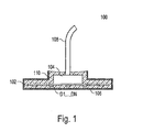
- Fig. 1 the basic structure of an LED lighting module 100 is shown schematically in longitudinal section. It has an AC-powered arrangement of a number of series-connected light emitting diodes D1, ..., DN, which are applied as a so-called LED dice on a printed circuit board 102 in a "chip-on-board” (COB) technology.
- COB chip-on-board
- the invention can also be applied to the driving of other configurations of LEDs and in particular a single LED.
- the heat-conductive, ceramic circuit board 102 of the LED lighting module 100 via a direct mains power supply consisting of a power supply 104 and a led out of the power supply 104 connection cable, plug and / or socket 108 for connection to an AC power.
- the light-emitting diodes D1,..., DN are accommodated in a transparent housing 106 with a highly transparent polymer mass 110 serving as an optically active lens surface for protection against mechanical damage.
- the LED illumination module 100 also has so-called Fresnel lenses in the form of a lens plate, which centrically above a each light-emitting diode D1, ..., DN are positioned within the transparent housing 106 and adhesively bonded laterally.
- the individual unhoused LED dice D1,..., DN are injection-molded directly with the highly transparent polymer mass 110 as part of an injection molding process or another suitable casting process.
- the polymer mass 110 consists of a thermally highly conductive material, which acts electrically insulating.
- the addition of a color conversion agent into the polymer mass 110 in the region of the main beam direction above the position monochromatic photon radiation in the spectral range of the color of blue emitting light emitting diodes D1, ..., DN is provided.
- the overall height of the overall arrangement of the LED lighting module 100 according to the invention is not more than, for example, 1.0 cm.
- the individual light-emitting diodes D1,..., DN are dimmable, wherein a control via radio or infrared signals or a microcontroller connected to a bus is conceivable for dimming the brightness of the photon radiation emitted by them.
- the power supply 104 for ensuring a direct mains power supply of the printed circuit board 102 can be operated according to the invention in a voltage input range of 100 V to 277 V. It can also be provided that the power supply 104 is operable with both AC voltage and DC voltage and in addition to the operation of individual LEDs for the Operation with serial as well as for operation with parallel-connected light-emitting diodes D1, ..., DN can be used.
- the inner sides of the transparent housing 106 (with the exception of the light-emitting region) according to the invention consist of a thermally highly conductive material, which is coated on the outside for heat dissipation of an electrically non-conductive material.
- the transparent housing 106 can be contacted by means of a plug, socket and / or connecting cable 108 led out of the housing laterally.
- each individual as a LED-formed light-emitting diode D1, ..., DN a parabolic or funnel-shaped, consisting of a thermally highly conductive, highly reflective material existing reflector of a reflector plate on the bottom is electrically insulated, is placed from above on the circuit board 102.
- Each reflector consists of a plastic with mirrored inside.
- the rear side of the printed circuit board 102 is coupled according to the invention to a heat sink, which is used for transmitting the heat generated during operation of the LED lighting module 100 to the housing 106 or a holder (not shown).
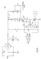
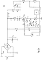
- a rectifier full-bridge circuit V1 rectifies the positive and / or negative half-circuits of the alternating current I mains supplied by a power supply network .
- At the storage capacitor connected to the ground node C1 at the output gate of the rectifier full bridge V1 is thus a varying with the mains voltage U network , smoothed and rectified DC link voltage U C1 .
- this first electronically controllable switching stage becomes electrically conductive, so that a drain current begins to flow which, as a result of the Energy storage acting storage inductor L1 continuously increases and flows as a diode current I D through the light emitting diodes D1, ..., DN.
- the increase of this diode current I D when charging the storage inductor L1 is detected by a first low-impedance shunt resistor R5, which is also arranged in the load circuit of the first power switch M1 and in the control circuit of the second power switch Q1 and connected to the ground node.
- a time-dependent control can also be provided for switching between the charging and discharging processes taking place in the storage inductor L1.
- This shunt measuring resistor R5 can preferably be designed as a potentiometer for dimming the light intensity I V [mcd] (ie the brightness) proportional to the diode current I D [mA] of the photon radiation emitted by the light-emitting diodes D1,..., DN.
- the semiconductor power switch Q1 becomes electrically conductive so that a collector current I C begins to flow and the gate voltage U G of the first electronically controllable switching stage M1 temporarily drops to "low" level, whereby in turn, the switching stage M1 is briefly blocked.
- the falling of the low impedance shunt measuring resistor R4 voltage U R4 serves for detection of the area bounded by the switching threshold of the second electronically controllable switch circuit Q1 to a minimum value falling of the current flowing through the light emitting diodes D1, ..., DN diode current I D in the free-running current path.
- both the charging and discharging current I L1 of the inductive reactance X L1 flows as diode current I D through the arrangement of the series-connected light emitting diodes D1, ..., DN of the LED illumination module 100 according to the invention, so that a periodically about an average oscillating, triangular current through the LED results.
- the tapped in the feedback path of the second measuring resistor R4, flowing through the light-emitting diodes D1, ..., DN current I D to the control input of the first switching stage M1 for galvanic decoupling (potential separation) of the voltage drop across the second measuring resistor R4 voltage U R4 and the Control voltage U G of the first switching stage M1 used signal transmission element U1 can preferably be used as an optocoupler diode (see. Fig. 2a ) or as level offset stage (cf. Fig. 2b ) be formed.
- a zener diode Z1 serves as a voltage limiter for stabilizing the control voltage U G of the first electronically controllable semiconductor power transistor M1 which can be tapped off at the output terminals of the optocoupler diode or level offset stage U1.
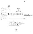
- Fig. 3 the temporal course of the current flowing through the light emitting diodes D1, ..., DN diode current I D is mapped. It is, as shown, to a periodically fluctuating around an average, triangular alternating current whose frequency through the switching thresholds required to control the two power transistors M1 and Q1 control voltages U G and U BE , the size of the inductance of the light emitting diodes D1 , ..., DN upstream inductor L1 and the instantaneous value of the voltage drop across the storage capacitor C1 DC link voltage U C1 is determined.
- these parameters were dimensioned so that the resulting diode current I D preferably has a frequency of less than 100 kHz.
- the DC offset forming the mean value of the diode current I D obtained can be set by suitably dimensioning the two shunt measurement resistors R 4 and R 5 in order to adapt the current source to the respective LED. In this way, a cost-effective adaptation of the diode current I D is made possible to different LEDs without circuitry additional measures.
- the solution according to the invention is much more space-saving.
- user-specific integrated circuits English: “application-specific integrated circuits", ASICs
- ASICs application-specific integrated circuits
- No. circuit symbol 100 LED lighting strip system comprising a powered via a power supply network with alternating current I grid arrangement of a plurality of series connected light emitting diodes D1, ..., DN, the (COB) technology on a circuit board in a "chip-on-board" as LED Dice are upset 102 thermally conductive, ceramic circuit board 104 Power supply for ensuring a direct mains power supply of the printed circuit board 104 106 transparent housing for protecting the printed circuit board 102 and the light-emitting diodes D1, ..., DN mounted thereon as LED dice from mechanical damage 108 laterally led out of the supply part 104 connecting cable, plug and / or socket for connection to an AC power supply 110 serving as the optically active lens surface highly transparent polymer composition, introduced into the transparent housing 108th 200a First variant of the control circuit according to the invention for providing a regulated power supply for a powered via a power grid with AC I network arrangement of several as a LED dice on a printed circuit board 102 applied, connected in series Lumineszenz
- Potential offset stage realized as a bipolar pnp transistor T2 second transistor stage for the in the context of the second variant of the control circuit 200b according to the invention as a signal transmission element U1 provided level or.
- Potential offset stage realized as bipolar npn transistor U1 Signal transmission member in the feedback branch of the tapped at the second measuring resistor R4, flowing through the high-power light emitting diodes D1, ..., DN current I D to the control input of the first switching stage M1 for galvanic decoupling (potential separation) of the voltage drop across the second measuring resistor R4 voltage U R4 and the control voltage U G of the first switching stage M1, realized as an optocoupler diode (see. Fig. 2a ) or as a level or potential offset stage (cf.
- V1 Rectifier full-bridge for rectifying the positive and / or negative half-circuits of the mains supplied by a power grid alternating current I network X L1 Inductive reactance of a coil L1, as a ballast choke for filtering harmonics in series with the high-performance light emitting diodes D1, ..., DN, to extend the current flow duration of the current flowing through the high-power light emitting diodes D1, ..., DN current I D Z1 Zener diode as a voltage limiter for stabilizing the input voltage U Z1 at the output terminals 3 and 4 of the optocoupler diode, level and potential offset stage U1 uP Microprocessor for controlling the series resistance R3 designed as a potentiometer for dimming the high-power light-emitting diodes D1,..., DN
Landscapes
- Physics & Mathematics (AREA)
- Electromagnetism (AREA)
- Circuit Arrangement For Electric Light Sources In General (AREA)
- Led Devices (AREA)
- Luminescent Compositions (AREA)
- Credit Cards Or The Like (AREA)
- Control Of El Displays (AREA)
Abstract
Description
Die vorliegende Erfindung bezieht sich auf eine Stromversorgung für LEDs. Dabei kommt ein Wandlerprinzip zur Anwendung, das einen periodisch um einen Gleichstromwert schwankenden, dreieckförmigen Wechselstrom durch die Lumineszenzdioden erzeugt. Durch dieses Verfahren wird dafür gesorgt, dass sowohl der Lade- als auch der Entladestrom eines induktiven Blindwiderstands im Lastkreis als Diodenstrom durch die Lumineszenzdioden fließt.The present invention relates to a power supply for LEDs. In this case, a transducer principle is used which generates a periodically fluctuating by a DC value, triangular alternating current through the light emitting diodes. By this method it is ensured that both the charging and the discharge of an inductive reactance in the load circuit as a diode current flows through the light emitting diodes.
Hochleistungsfähige lichtemittierende Halbleiter-Lumineszenzdioden (engl.: "Light-Emitting Diodes", LEDs), kurz Leuchtdioden genannt, haben schon lange ihren Platz in vielen Bereichen erobert, in denen ein Bedarf an optischen Anzeigesystemen oder Beleuchtungssystemen mit geringem Energieverbrauch besteht, wie z.B. in der Verkehrs- und Signaltechnik. Durch entscheidende technische Innovationen im Bereich der lichtemittierenden Halbleiter-Bauelemente, mit Hilfe derer heute eine höhere Lichtausbeute sowie eine Ausweitung des Farbspektrums auf den gesamten Wellenlängenbereich des sichtbaren Lichts zwischen 780 nm (violett) und 380 nm (dunkelrot) erreichbar ist, erschließt sich der Optoelektronik lichttechnisch ein völlig neuer Markt.High-performance light emitting diodes (LEDs), or light-emitting diodes, have long since gained their place in many fields where there is a need for low-power optical display systems or lighting systems, e.g. in traffic and signaling technology. Key technological innovations in the field of light-emitting semiconductor devices, which nowadays enable higher luminous efficacy and an expansion of the color spectrum over the entire wavelength range of visible light between 780 nm (violet) and 380 nm (dark red), open up for optoelectronics technically a completely new market.
Zur Erzielung einer gleichmäßigen Ausleuchtung von Flächen werden dabei in der Regel Streuscheiben verwendet. Aufgrund des Netzbetriebes, vor allem bei Anwendungen im Außenbereich, sind üblicherweise Leuchtengehäuse erforderlich, um die verwendeten elektronischen Bauteile vor dem Eindringen von Feuchtigkeit zu schützen.To achieve a uniform illumination of surfaces usually lenses are used. Due to the network operation, especially in outdoor applications, usually housing lights are required to protect the electronic components used from the ingress of moisture.
Um die zentrale Idee der vorliegenden Erfindung zu verstehen, soll im Folgenden kurz auf die wichtigsten Merkmale konventioneller Verfahren und Technologien nach dem Stand der Technik zur Herstellung von Halbleiter-Lumineszenzdioden eingegangen werden, vor allem auf die sogenannte "Chip-on-Board" (COB)-Technologie, welche in den letzten Jahren stark an Bedeutung gewonnen hat.In order to understand the central idea of the present invention, the main features of conventional methods and technologies according to the state of the art for the production of semiconductor light-emitting diodes will be briefly discussed below, in particular the so-called "chip-on-board" (COB ) Technology, which has become increasingly important in recent years.
Bei der "Chip-on-Board" (COB)-Technologie wird der, rohe LED-Chip mit der Struktur und den Anschlüssen nach oben (engl.: "face up") mit Leitkleber auf der Leiterplatte angebracht. Dieser Vorgang wird im angloamerikanischen Sprachgebrauch als "Die Bonding" bezeichnet. Nach dem Aushärten des Klebers erfolgt in einem zusätzlichen Arbeitsschritt das Verbinden der Chipanschlüsse mit der Leiterplatte mit Hilfe eines aus der Herstellung integrierter Schaltungen bekannten Wire-Bonders. Dabei werden die einzelnen Chipanschlüsse und die Leiterplatte mit einem Golddraht verbunden. Durch die Verwendung von speziellen Leiterplatten-Materialien können hervorragende Wärmeleiteigenschaften erreicht werden. Daraus resultiert eine längere Lebensdauer und eine höhere Lichtausbeute pro Fläche. Nach Aufbringung einer polymeren Schicht ist das LED-Array vor mechanischer Beschädigung durch Erschütterung oder Vibrationen geschützt. Spezielle Leiterplatten mit Reflektorschichten dienen dabei zur Lichtbündelung und Erhöhung der Lichtstärken bei kleineren Abstrahlwinkeln.In "chip-on-board" (COB) technology, the raw LED chip with the structure and the terminals is mounted face-up with conductive adhesive on the circuit board. This process is referred to in Anglo-American usage as "the bonding". After curing of the adhesive takes place in an additional step connecting the chip terminals to the circuit board using a known from the production of integrated circuits wire bonder. The individual chip connections and the circuit board are connected with a gold wire. By using special printed circuit board materials excellent thermal conduction properties can be achieved. This results in a longer life and a higher light output per area. After application of a polymeric layer, the LED array is protected from mechanical damage by shock or vibration. Special printed circuit boards with reflector layers serve for light bundling and increasing the light intensities at smaller radiation angles.
Im Vergleich zu herkömmlichen LED-Modulen können somit durch Verwendung von Lumineszenzdioden, die mittels COB-Technologie als LED-Arrays auf einer Leiterplatte aufgebracht sind, effiziente Beleuchtungseinheiten hoher Lichtausbeute, langer Lebensdauer, platzsparender Bauweise und einem relativ geringen Kostenaufwand hergestellt werden. Aufgrund der erreichbaren Lichtstromwerte sind diese Module nicht nur als Signal- und Hinterbeleuchtungen interessant, sondern können direkt als Beleuchtungsmittel eingesetzt werden. In COB-Technologie hergestellte LED-Arrays mit einem Abstrahlwinkel von 180° erlauben eine helle Ausleuchtung von Flächen mit einer homogenen Lichtverteilung, die mit der Ausleuchtung durch eine mit 40 bis 50 mA betriebenen Beleuchtungsanlage mit Leuchtstofflampen vergleichbar ist. Ein weiterer Pluspunkt ist der um 50 % geringere Stromverbrauch gegenüber einer derartigen Beleuchtungsanlage.Compared to conventional LED modules can thus by using light emitting diodes, which are applied by means of COB technology as LED arrays on a circuit board, efficient lighting units high luminous efficacy, long life, space-saving design and a relatively low cost can be produced. Due to the achievable luminous flux values, these modules are not just signal and Rear lighting interesting, but can be used directly as a means of lighting. COB-technology LED arrays with a 180 ° beam angle allow for bright illumination of surfaces with a homogeneous light distribution comparable to the illumination of a 40 to 50 mA fluorescent lighting system. Another advantage is the 50% lower power consumption compared to such a lighting system.
Aus hochleistungsfähigen Lumineszenzdioden aufgebaute Punktlichtquellen in COB-Technologie eignen sich ideal für kleine Arbeits- und Leseleuchten, als flexibel nutzbare Lichtquellen in Spotbeleuchtungen, als zentrale Lichtquelle für Orientierungsleuchten etc.Point light sources made of high-performance light-emitting diodes in COB technology are ideal for small work and reading lights, as flexibly usable light sources in spotlights, as a central light source for orientation lights, etc.
Aus der Offenlegungsschrift
Bei herkömmlichen Kondensatornetzteilen nach dem Stand der Technik kann (im Gegensatz zu der erfindungsgemäßen elektronischen Lösung) der Effektivwert der Eingangswechselspannung variabel gewählt werden (z.B. zwischen 100 VAC und 277 VAC); sogar eine Versorgung des Netzteils mit Gleichspannung ist möglich.In conventional capacitor power supplies according to the prior art can be chosen to be variable the effective value of the input AC voltage (for example between 100 V AC and 277 V AC) (in contrast to the inventive electronic solution); even a supply of the power supply with DC voltage is possible.
Da jedoch bei einer Kondensatornetzteilschaltung die Größe der verwendeten Kondensatoren mit steigender Betriebsleistung stark zunimmt, können mit einem derartigen Netzteil nur ge ringe Leistungen bei akzeptabler Baugröße realisiert werden. Zudem verschlechtert sich die Leistung der in Kondensatornetzteilen üblicherweise verwendeten Elektrolytkondensatoren mit der Zahl der Betriebsstunden. Aus den vorstehend genannten Gründen ist für den Betrieb von Hochleistungs-LEDs (mit einer Betriebsleistung von bis zu 4 W) der Einsatz alternativer elektronischer Lösungen erforderlich.However, since in a capacitor power supply circuit, the size of the capacitors used with increasing operating power increases sharply, with such a power supply only ge achievements with an acceptable size. In addition, the performance of the electrolytic capacitors commonly used in capacitor power supplies deteriorates with the number of operating hours. For the reasons mentioned above, the use of high-power LEDs (with an operating power of up to 4 W) requires the use of alternative electronic solutions.
Neben den oben beschriebenen Aufgaben, soll die vorliegende Erfindung eine Stromversorgung für Lumineszenzdioden bereitstellen, die in einfacher Weise auf unterschiedliche LEDs angepasst werden kann. Darüber hinaus soll natürlich auch ein guter Wirkungsgrad erreicht werden. In addition to the objects described above, the present invention is intended to provide a power supply for light-emitting diodes, which can be easily adapted to different LEDs. In addition, of course, a good efficiency should be achieved.
Diese Aufgabe wird erfindungsgemäß durch die Merkmale der unabhängigen Patentansprüche gelöst. Vorteilhafte Ausführungsbeispiele, die den Gedanken der Erfindung weiterbilden, sind in den abhängigen Patentansprüchen definiert.This object is achieved by the features of the independent claims. Advantageous embodiments which further develop the idea of the invention are defined in the dependent claims.
Die vorliegende Erfindung nach Anspruch 1 offenbart eine Stromversorgung für wenigstens eine über ein Stromversorgungsnetz mit Wechselstrom gespeiste Lumineszenzdiode, aufweisend mindestens einen als Speicherdrossel in Serie zu der Lumineszenzdiode geschalteten induktiven Blindwiderstand, Schaltstufen zur Umschaltung zwischen den in der Speicherdrossel ablaufenden Lade- bzw. Entladevorgängen bei Über- bzw. Unterschreiten von Schwellwerten ihrer jeweiligen Steuerspannungen, einen parallel zur Serienschaltung der Lumineszenzdioden und der Speicherdrossel geschalteten freilaufenden Strompfad für wenigstens einen Teil des von der Speicherdrossel bei Sperrung der ersten Schaltstufe an die Lumineszenzdioden abgegebenen Entladestroms, sowie einen Nebenschluss-Messwiderstand zur Erfassung des durch die Lumineszenzdioden während eines in der Speicherdrossel ablaufenden Entladevorgangs fließenden Diodenstroms.The present invention according to claim 1 discloses a power supply for at least one powered by a power supply network with alternating luminescence diode, comprising at least one as a storage inductor in series with the light emitting diode connected inductive reactance, switching stages for switching between the running in the storage choke loading and unloading operations when or undershooting threshold values of their respective control voltages, a free-running current path connected in parallel with the series connection of the light-emitting diodes and the storage choke for at least a portion of the discharge current delivered by the storage choke upon blocking of the first switching stage to the light-emitting diodes, and a shunt measuring resistor for detecting the leakage current the light-emitting diodes during a discharging process running in the storage choke discharge diode current.
Bei Verwendung des erfindungsgemäßen Schaltungsprinzips können auch mehrere in Serie geschaltete Lumineszenzdioden an Niedervoltspannungen von mehr als 30 V angeschlossen werden. Die Regelschaltung wirkt dabei als Konstantstromquelle.When using the circuit principle according to the invention, several series-connected light-emitting diodes can be connected to low-voltage voltages of more than 30 V. The control circuit acts as a constant current source.
Das mit Hilfe dieser Regelschaltung realisierte Verfahren arbeitet nach einem Wandlerprinzip, bei dem ein periodisch um einen Gleichstromwert schwankender, dreieckförmiger Strom durch die LED fließt. Dabei ist mit Hilfe einer schaltungstechnischen Maßnahme dafür gesorgt, dass sowohl der Lade- als auch der Entladestrom eines als Speicherdrossel in Serie zu den Lumineszenzdioden geschalteten induktiven Blindwiderstands als Diodenstrom durch die Lumineszenzdioden fließt.The realized with the help of this control circuit operates on a converter principle in which a periodically fluctuates by a DC value, triangular current flows through the LED. It is ensured by means of a circuit measure that both the charging and the discharge of a connected as a storage inductor in series with the light-emitting diodes inductive reactance as a diode current flows through the light emitting diodes.
Der Vorteil dieses Verfahrens gegenüber dem Stand der Technik besteht in der Bereitstellung einer Schaltung, mit der eine kontinuierliche Messung des Diodenstroms erfolgen kann. Zusätzlich erfolgt eine Reduzierung der Gesamtverlustleistung des LED-Beleuchtungsmoduls. The advantage of this method over the prior art is the provision of a circuit with which a continuous measurement of the diode current can take place. In addition, there is a reduction in the total power loss of the LED lighting module.
Weitere Eigenschaften, Merkmale, Vorteile und Zweckmäßigkeiten der zugrunde liegenden Erfindung resultieren aus den untergeordneten abhängigen Patentansprüchen, welche nunmehr, bezugnehmend auf die Figuren der begleitenden Zeichnungen und anhand einer detaillierten Beschreibung eines Ausführungsbeispiels der zugrunde liegenden Erfindung, erläutert werden sollen. Hierbei zeigen:
- Fig. 1
- ein LED-Beleuchtungsmodul, bestehend aus einer über ein Stromversorgungsnetz mit Wechselstrom gespeisten Anordnung mehrerer in Serie geschalteter Lumineszenzdioden, die auf einer Leiterplatte in einer "Chip-on-Board" (COB)-Technologie als LED-Dice aufgebracht sind,
- Fig. 2a
- eine erste Variante einer Regelschaltung zur Bereitstellung einer geregelten Stromversorgung für LEDs, bei der ein im Rückkopplungszweig zur galvanischen Entkopplung (Potenzialtrennung) verwendete Signalübertragungsglied als Optokopplerdiode realisiert ist,
- Fig. 2b
- eine zweite Variante der erfindungsgemäßen Regelschaltung zur Bereitstellung einer geregelten Stromversorgung für LEDs, bei der ein im Rückkopplungszweig zur galvanischen Entkopplung (Potenzialtrennung) verwendete Signalübertragungsglied als Pegel- bzw. Potenzialversatzstufe realisiert ist und
- Fig. 3
- den Zeitverlauf des durch eine Lumineszenzdiode fließenden Stromes.
- Fig. 1
- an LED lighting module, consisting of an AC-powered arrangement of a plurality of series-connected light-emitting diodes, which are mounted on a printed circuit board in a "chip-on-board" (COB) technology as an LED dice
- Fig. 2a
- a first variant of a control circuit for providing a regulated power supply for LEDs, in which a signal transmission element used in the feedback path for galvanic decoupling (electrical isolation) is implemented as an optocoupler diode,
- Fig. 2b
- a second variant of the control circuit according to the invention for providing a regulated power supply for LEDs, in which a used in the feedback path for galvanic decoupling (potential separation) signal transmission element is implemented as a level or potential offset stage and
- Fig. 3
- the time course of the current flowing through a light emitting diode current.
Im Folgenden werden die Funktionen der in einem Ausführungsbeispiel der vorliegenden Erfindung enthaltenen Baugruppen, wie in den
In
Es ist zu erwähnen, dass die optischen und mechanischen Eigenschaften des LED-Beleuchtungsmoduls nachIt should be noted that the optical and mechanical properties of the LED lighting module after
Die Erfindung lässt sich indessen ebenso auf die Ansteuerung anderer Konfigurationen von LEDs und insbesondere einer einzelnen LED anwenden.However, the invention can also be applied to the driving of other configurations of LEDs and in particular a single LED.
Nach einem Ausführungsbeispiel der Erfindung verfügt die wärmeleitende, keramische Leiterplatte 102 des LED-Beleuchtungsmoduls 100 über eine direkte Netzstromversorgung, bestehend aus einem Netzteil 104 und einem seitlich aus dem Netzteil 104 herausgeführten Anschlusskabel, Stecker und/oder Stecksockel 108 zum Anschluss an ein Wechselstromnetz. Die Lumineszenzdioden D1,...,DN sind dabei zum Schutz vor mechanischer Beschädigung in einem transparenten Gehäuse 106 mit einer als optisch aktive Linsenfläche dienenden hochtransparenten Polymermasse 110 untergebracht.According to one embodiment of the invention, the heat-conductive,
Zur Erzielung einer gebündelten, homogenen Lichtverteilung im Bereich der Hauptstrahlrichtungen der einzelnen Lumineszenzdioden D1,...,DN verfügt das erfindungsgemäße LED-Beleuchtungsmodul 100 darüber hinaus über sogenannte Fresnel-Linsen in Form einer Linsenplatte, welche zentrisch oberhalb einer jeden Lumineszenzdiode D1,...,DN innerhalb des transparenten Gehäuses 106 positioniert und seitlich verklebt sind.To achieve a bundled, homogeneous light distribution in the region of the main beam directions of the individual light-emitting diodes D1,..., DN, the
Um auf der Seite der Leiterplatte 102, auf der die Lumineszenzdioden D1,...,DN aufgebracht sind, beim Vergießen der hochtransparenten Polymermasse 110 innerhalb des transparenten Gehäuses 106 die Entstehung von Luftblasen zu vermeiden, sind auf der Leiterplatte 102 Löcher eingebracht. Bei der Herstellung des LED-Beleuchtungsmoduls 100 werden die einzelnen ungehäusten LED-Dice D1,...,DN im Rahmen eines Spritzgussverfahrens oder eines anderen geeigneten Gießverfahrens direkt mit der hochtransparenten Polymermasse 110 umspritzt. Die Polymermasse 110 besteht dabei aus einem thermisch gut leitenden Material, das elektrisch isolierend wirkt.In order to avoid the formation of air bubbles on the side of the printed
Da weißes Licht mit Hilfe einzelner Lumineszenzdioden nicht erzeugt werden kann, ist erfindungsgemäß die Zugabe eines Farbkonversionsmittels in die Polymermasse 110 im Bereich der Hauptstrahlrichtung oberhalb der Position monochromatische Photonenstrahlung im Spektralbereich der Farbe blau emittierender Lumineszenzdioden D1,...,DN vorgesehen.Since white light can not be generated with the aid of individual light emitting diodes, according to the invention the addition of a color conversion agent into the
Aufgrund einer platzsparenden Anordnung der verwendeten Bauteile und der Verwendung des oben erwähnten effizienten COB-Herstellungsverfahrens beträgt die Bauhöhe der Gesamtanordnung des erfindungsgemäßen LED-Beleuchtungsmoduls 100 nicht mehr als beispielsweise 1,0 cm.Due to a space-saving arrangement of the components used and the use of the above-mentioned efficient COB manufacturing process, the overall height of the overall arrangement of the
Nach einem Ausführungsbeispiel der zugrunde liegenden Erfindung sind die einzelnen Lumineszenzdioden D1,...,DN dimmbar, wobei zur Dimmung der Helligkeit der von ihnen emittierten Photonenstrahlung eine Ansteuerung über Funk- oder Infrarotsignale bzw. einen an einen Bus angeschlossenen Mikrocontroller denkbar ist.According to one embodiment of the underlying invention, the individual light-emitting diodes D1,..., DN are dimmable, wherein a control via radio or infrared signals or a microcontroller connected to a bus is conceivable for dimming the brightness of the photon radiation emitted by them.
Das Netzteil 104 zur Gewährleistung einer direkten Netzstromversorgung der Leiterplatte 102 kann erfindungsgemäß in einem Spannungseingangsbereich von 100 V bis 277 V betrieben werden. Es kann dabei auch vorgesehen sein, dass das Netzteil 104 sowohl mit Wechselspannung als auch mit Gleichspannung betreibbar ist und neben dem Betrieb einzelner LEDs für den Betrieb mit seriell als auch für den Betrieb mit parallel geschalteten Lumineszenzdioden D1,...,DN verwendet werden kann.The
Die Innenseiten des transparenten Gehäuses 106 (mit Ausnahme des lichtemittierenden Bereiches) bestehen erfindungsgemäß aus einem thermisch gut leitenden Material, das auf der Außenseite zur Wärmeabfuhr von einem elektrisch nicht leitenden Material überzogen ist. Dabei kann das transparente Gehäuse 106 mit Hilfe eines seitlich aus dem Gehäuse herausgeführten Steckers, Stecksockels und/oder Anschlusskabels 108 kontaktiert werden.The inner sides of the transparent housing 106 (with the exception of the light-emitting region) according to the invention consist of a thermally highly conductive material, which is coated on the outside for heat dissipation of an electrically non-conductive material. In this case, the
Nach einem Ausführungsbeispiel der zugrunde liegenden Erfindung ist dabei vorgesehen, dass um jede einzelne, als LED-Die ausgebildete Lumineszenzdiode D1,...,DN ein parabolisch oder trichterförmig ausgeformter, aus einem thermisch gut leitfähigen, hochreflektierenden Material bestehender Reflektor einer Reflektorplatte, die auf der Unterseite elektrisch isoliert ist, von oben auf die Leiterplatte 102 aufgesetzt ist. Jeder einzelne Reflektor besteht dabei aus einem Kunststoff mit verspiegelter Innenseite.According to one embodiment of the underlying invention, it is provided that around each individual, as a LED-formed light-emitting diode D1, ..., DN a parabolic or funnel-shaped, consisting of a thermally highly conductive, highly reflective material existing reflector of a reflector plate on the bottom is electrically insulated, is placed from above on the
Die Rückseite der Leiterplatte 102 ist erfindungsgemäß an einen Kühlkörper angekoppelt, welcher zur Übertragung der beim Betrieb des LED-Beleuchtungsmoduls 100 entstehenden Abwärme auf das Gehäuse 106 oder eine Halterung (nicht dargestellt) dient.The rear side of the printed
Bezugnehmend auf
Über eine Gleichrichter-Vollbrückenschaltung V1 werden die positiven und/oder negativen Netzhalbwellen des von einem Stromversorgungsnetz gelieferten Wechselstroms I Netz gleichgerichtet. An dem mit dem Masseknoten verbundenen Speicherkondensator C1 am Ausgangstor der Gleichrichter-Vollbrücke V1 liegt somit eine mit der Netzspannung U Netz variierende, geglättete und gleichgerichtete Zwischenkreisspannung U C1 an.A rectifier full-bridge circuit V1 rectifies the positive and / or negative half-circuits of the alternating current I mains supplied by a power supply network . At the storage capacitor connected to the ground node C1 at the output gate of the rectifier full bridge V1 is thus a varying with the mains voltage U network , smoothed and rectified DC link voltage U C1 .
Nach dem Anlegen einer geeignet dimensionierten Steuerspannung U G an das Gate eines beispielsweise als selbstsperrender n-Kanal-MOS-Feldeffekttransistor realisierten ersten Halbleiter-Leistungsschalters M1 wird diese erste elektronisch steuerbare Schaltstufe elektrisch leitend, so dass ein Drainstrom zu fließen beginnt, der infolge der als Energiespeicher wirkenden Speicherdrossel L1 kontinuierlich ansteigt und als Diodenstrom I D durch die Lumineszenzdioden D1,...,DN hindurchfließt. Der Anstieg dieses Diodenstroms I D bei Ladung des Speicherdrossel L1 wird von einem ersten niederohmigen Nebenschluss-Messwiderstand R5 erfasst, der zugleich im Lastkreis des ersten Leistungsschalters M1 sowie im Steuerkreis des zweiten Leistungsschalters Q1 angeordnet und mit dem Masseknoten verbunden ist. Neben den beiden Leistungsschaltern M1 und Q1 kann erfindungsgemäß auch eine zeitabhängige Steuerung zur Umschaltung zwischen den in der Speicherdrossel L1 ablaufenden Lade- bzw. Entladevorgängen vorgesehen sein.After the application of a suitably dimensioned control voltage U G to the gate of a first semiconductor power switch M1 implemented, for example, as a normally-off n-channel MOS field-effect transistor, this first electronically controllable switching stage becomes electrically conductive, so that a drain current begins to flow which, as a result of the Energy storage acting storage inductor L1 continuously increases and flows as a diode current I D through the light emitting diodes D1, ..., DN. The increase of this diode current I D when charging the storage inductor L1 is detected by a first low-impedance shunt resistor R5, which is also arranged in the load circuit of the first power switch M1 and in the control circuit of the second power switch Q1 and connected to the ground node. In addition to the two power switches M1 and Q1, according to the invention, a time-dependent control can also be provided for switching between the charging and discharging processes taking place in the storage inductor L1.
Dieser Nebenschluss-Messwiderstand R5 kann dabei vorzugsweise als Potentiometer zur Dimmung der dem Diodenstrom I D [mA] proportionalen Lichtstärke IV [mcd] (d.h. der Helligkeit) der von den Lumineszenzdioden D1,...,DN emittierten Photonenstrahlung ausgebildet sein.This shunt measuring resistor R5 can preferably be designed as a potentiometer for dimming the light intensity I V [mcd] (ie the brightness) proportional to the diode current I D [mA] of the photon radiation emitted by the light-emitting diodes D1,..., DN.
Sobald nun die Basis-Emitter-Spannung U BE einer z.B. als bipolarer npn-Transistor ausgebildeten zweiten elektronisch steuerbaren Schaltstufe Q1 eine bestimmte Schaltschwelle erreicht, wird der Halbleiter-Leistungsschalter Q1 elektrisch leitend, so dass ein Kollektorstrom I C zu fließen beginnt und die Gatespannung U G der ersten elektronisch steuerbaren Schaltstufe M1 vorübergehend auf "Low"-Pegel absinkt, wodurch wiederum die Schaltstufe M1 kurzzeitig gesperrt wird. Dies hat zur Folge, dass der über die Speicherdrossel L1 aufgebaute Diodenstrom I D durch eine Freilaufdiode DF und einen zu dieser in Serie geschalteten zweiten niederohmigen Nebenschluss-Messwiderstand R4 im Parallelzweig zur Serienschaltung der Lumineszenzdioden D1,...,DN und dem durch die Speicherdrossel L1 gebildeten induktiven Blindwiderstand XL1 abgeleitet wird.As soon as the base-emitter voltage U BE of a second electronically controllable switching stage Q1 designed as bipolar npn transistor, for example, reaches a certain switching threshold, the semiconductor power switch Q1 becomes electrically conductive so that a collector current I C begins to flow and the gate voltage U G of the first electronically controllable switching stage M1 temporarily drops to "low" level, whereby in turn, the switching stage M1 is briefly blocked. This has the consequence that the diode current I D built up via the storage inductor L1 is connected through a freewheeling diode DF and a second low-resistance shunt resistor R4 connected in series to the series connection of the light-emitting diodes D1,..., DN and through the storage inductor L1 formed inductive reactance X L1 is derived.
Mit Hilfe dieser verhältnismäßig einfachen schaltungstechnischen Maßnahme wird eine Gefährdung des ersten Halbleiter-Leistungstransistors M1 durch die beim Abschalten des Drainstroms I D (beim Sperren von M1) am induktiven Blindwiderstand XL1 abfallende Induktionsspannung U L1 vermieden, die ein Vielfaches der Betriebsspannung betragen kann.With the help of this relatively simple circuit measure a danger to the first semiconductor power transistor M1 by the turning off the drain current I D (when blocking M1) at the inductive reactance X L1 falling induction voltage U L1 is avoided, which can be a multiple of the operating voltage.
Die an dem niederohmigen Nebenschluss-Messwiderstand R4 abfallende Spannung U R4 dient dabei zur Erfassung des durch die Schaltschwelle der zweiten elektronisch steuerbaren Schaltstufe Q1 auf einen Minimalwert begrenzten Absinkens des durch die Lumineszenzdioden D1,...,DN fließenden Diodenstroms I D im freilaufenden Strompfad.The falling of the low impedance shunt measuring resistor R4 voltage U R4 serves for detection of the area bounded by the switching threshold of the second electronically controllable switch circuit Q1 to a minimum value falling of the current flowing through the light emitting diodes D1, ..., DN diode current I D in the free-running current path.
Nach Rückkopplung des am zweiten Messwiderstand R4 abgegriffenen, durch die Lumineszenzdioden D1,...,DN fließenden Diodenstromes I D auf den Steuereingang der ersten Schaltstufe M1 über ein Signalübertragungsglied U1 zur galvanischen Entkopplung (Potenzialtrennung) der am zweiten Messwiderstand R4 abfallenden Spannung U R4 und der Gatespannung U G der ersten Schaltstufe M1 wirkt dieser übersetzte, abklingende Diodenstrom I D als "neuer" Gatestrom I G . Das hat zur Folge, dass die Gatespannung U G der ersten elektronisch steuerbaren Schaltstufe M1 auf dem Pegelwert "Low" verharrt und die Schaltstufe M1 daher so lange gesperrt bleibt, bis der Stromfluss durch das Signalübertragungsglied U1 unter eine bestimmte Schwelle abgesunken ist. Nachdem die Schaltstufe M1 wieder zu leiten begonnen hat, wird der oben beschriebene Vorgang in periodisch wiederkehrender Folge fortgesetzt.After feedback of the second measuring resistor R4 tapped, flowing through the light-emitting diodes D1, ..., DN diode current I D to the control input of the first switching stage M1 via a signal transmission element U1 for galvanic decoupling (potential separation) of the second measuring resistor R4 sloping voltage U R4 and the gate voltage U G of the first switching stage M1 acts this translated, decaying diode current I D as a "new" gate current I G. This has the consequence that the gate voltage U G of the first electronically controllable switching stage M1 remains at the level "low" and the switching stage M1 therefore remains disabled until the current flow through the signal transmission element U1 below a certain Threshold has dropped. After the switching stage M1 has started to conduct again, the process described above is continued in a periodically recurring sequence.
Bei dem erfindungsgemäßen Verfahren fließt also sowohl der Lade- als auch der Entladestrom I L1 des induktiven Blindwiderstands XL1 als Diodenstrom I D durch die Anordnung der seriell geschalteten Lumineszenzdioden D1,...,DN des erfindungsgemäßen LED-Beleuchtungsmoduls 100, so dass sich ein periodisch um einen Mittelwert pendelnder, dreieckförmiger Strom durch die LED ergibt.In the method according to the invention, therefore, both the charging and discharging current I L1 of the inductive reactance X L1 flows as diode current I D through the arrangement of the series-connected light emitting diodes D1, ..., DN of the
Das im Rückkopplungszweig des an dem zweiten Messwiderstand R4 abgegriffenen, durch die Lumineszenzdioden D1,...,DN fließenden Stromes I D auf den Steuereingang der ersten Schaltstufe M1 zur galvanischen Entkopplung (Potenzialtrennung) der an dem zweiten Messwiderstand R4 abfallenden Spannung U R4 und der Steuerspannung U G der ersten Schaltstufe M1 verwendete Signalübertragungsglied U1 kann dabei vorzugsweise als Optokopplerdiode (vgl.
Bei der Realisierung der zweiten Variante der erfindungsgemäßen Regelschaltung 200b mit Pegel- bzw. Potenzialversatzstufe U1 sind zusätzlich zu den für die erste Variante 200a mit Optokopplerdiode benötigten Bauelementen zwei Transistorstufen T1 und T2 sowie ein Spannungsteiler, der durch die beiden Widerstände R6 und R7 gebildet wird, erforderlich.In the realization of the second variant of the
In
Der den Mittelwert des erhaltenen Diodenstroms I D bildende Gleichstrom-Offset kann dabei durch eine geeignete Dimensionierung der beiden Nebenschluss-Messwiderstände R4 und R5 eingestellt werden, um die Stromquelle an die jeweilige LED anzupassen. Auf diese Weise wird eine kostengünstige Anpassung des Diodenstroms I D an unterschiedliche LEDs ohne schaltungstechnische Zusatzmaßnahmen ermöglicht.The DC offset forming the mean value of the diode current I D obtained can be set by suitably dimensioning the two shunt
Im Gegensatz zu herkömmlichen Kondensatornetzteilen nach dem Stand der Technik ist die erfindungsgemäße Lösung wesentlich platzsparender. Darüber hinaus sind auch anwenderspezifische integrierte Schaltungen (engl.: "Application-Specific Integrated Circuits", ASICs) mit einem vergleichsweise geringen Platzbedarf denkbar.In contrast to conventional capacitor power supplies according to the prior art, the solution according to the invention is much more space-saving. In addition, user-specific integrated circuits (English: "application-specific integrated circuits", ASICs) with a relatively small footprint are conceivable.
Claims (11)
- Power supply for at least one light emitting diode (D1, ..., DN) fed with alternating current (INetz ) via a current supply grid, having:- at least one inductive reactance (XL1) connected in series with the light emitting diode (D1, ..., DN) as a storage coil (L1),- switching stages (M1, Q1) for switching over between the charging procedures and discharging procedures occurring in the storage coil (L1) upon exceeding or undershooting values of their respective control voltages ( U G, U BE ),- a free-running current path, parallel to the series connection of the light emitting diodes (D1, ..., DN) and the storage coil (L1), for at least a part of the discharge current issued by the storage coil (L1) upon blocking of the first switching stage (M1) to the light emitting diodes (D1, ..., DN) , and- a shunt measurement resistance (R4) for detection of the diode current (ID ) flowing through the light emitting diodes (D1, ..., DN) during a discharging procedure occurring in the storage coil (L1).
- Power supply according to claim 1,
characterised by
a first shunt measurement resistance (R5) for detection of the diode current (ID ) flowing through the light emitting diodes (D1, ..., DN) during a charging procedure occurring in the storage coil (L1). - Power supply according to claim 2,
characterised in that,
the first shunt measurement resistance (R5) is adjustable for dimming the light emitting diodes (D1, ..., DN). - Power supply according to claim 1,
characterised by
a signal transmission member (U1), serving for the galvanic decoupling of the voltage dropping at the second measurement resistance (R4) and the control voltage ( U G ) of the first switching stage (M1), for feedback of the current (ID ) flowing through the light emitting diodes (D1, ..., DN), tapped off at the second measurement resistance (R4), to the control input of the first switching stage (M1). - Power supply according to claim 4,
characterised in that,
the signal transmission member (U1) used for potential separation is an optocoupler diode. - Power supply according to claim 4,
characterised in that,
the signal transmission member (U1) used for potential separation is a level offset stage. - Power supply according to any of claims 1 to 6,
characterised by
a Zener diode (Z1) as a voltage limiter for stabilization of the control voltage ( U G ), which can be tapped off at the output terminals of the optocoupler diode, level or potential offset stage (U1), of the first electronically controllable semiconductor power transistor (M1). - Power supply according to any of claims 1 to 7,
characterised by
a free-wheeling diode (DF) in the free-running current path, connected anti-parallel to the series connection of the light emitting diodes (D1, ..., DN) and the storage coil (L1). - Power supply according to any of claims 1 to 8,
characterised by
a potentiometer (R3) as a series resistance in the control circuit of the first semiconductor power transistor (M1) for dimming the light intensity (Iv ), proportional to the diode current (ID ), of the radiation emitted by the light emitting diodes (D1, ..., DN). - Power supply according to any of claims 1 to 9,
characterised by
a time-dependent control for switching over between the charging procedures and discharging procedures occurring in the storage coil (L1). - Method for regulated power supply of at least one light emitting diode (D1, ..., DN) fed with alternating current (INetz ) via a current supply grid,
characterised in that,
the charging procedures and discharging procedures occurring in the storage coil (Ll) are used for the production of an alternating current (ID ) flowing through the light emitting diodes (D1, ..., DN), varying periodically around an adjustable direct current value,
wherein at least the alternating current (ID ) flowing through the light emitting diodes (D1, ..., DN) during the charging procedures and discharging procedures is detected, and
wherein the direct current offset forming the mean value of the resulting triangular diode current (ID ) is set by means of at least one shunt measurement resistance (R4, R5).
Priority Applications (3)
| Application Number | Priority Date | Filing Date | Title |
|---|---|---|---|
| EP06010830A EP1691582A3 (en) | 2002-07-04 | 2003-06-30 | Power supply for LEDs |
| EP08164999.8A EP2001269B1 (en) | 2002-07-04 | 2003-06-30 | Electricity supply for luminescence diodes |
| EP10184377A EP2262347A1 (en) | 2002-07-04 | 2003-06-30 | Power supply for light emitting diodes |
Applications Claiming Priority (3)
| Application Number | Priority Date | Filing Date | Title |
|---|---|---|---|
| DE10230103 | 2002-07-04 | ||
| DE10230103A DE10230103B4 (en) | 2002-07-04 | 2002-07-04 | Power supply for light-emitting diodes |
| PCT/EP2003/006952 WO2004006629A2 (en) | 2002-07-04 | 2003-06-30 | Power supply unit for light-emitting diodes |
Related Child Applications (2)
| Application Number | Title | Priority Date | Filing Date |
|---|---|---|---|
| EP08164999.8A Division EP2001269B1 (en) | 2002-07-04 | 2003-06-30 | Electricity supply for luminescence diodes |
| EP06010830A Division EP1691582A3 (en) | 2002-07-04 | 2003-06-30 | Power supply for LEDs |
Publications (2)
| Publication Number | Publication Date |
|---|---|
| EP1520449A2 EP1520449A2 (en) | 2005-04-06 |
| EP1520449B1 true EP1520449B1 (en) | 2008-08-20 |
Family
ID=29723706
Family Applications (4)
| Application Number | Title | Priority Date | Filing Date |
|---|---|---|---|
| EP03762563A Expired - Lifetime EP1520449B1 (en) | 2002-07-04 | 2003-06-30 | Power supply unit for light-emitting diodes |
| EP10184377A Ceased EP2262347A1 (en) | 2002-07-04 | 2003-06-30 | Power supply for light emitting diodes |
| EP08164999.8A Expired - Lifetime EP2001269B1 (en) | 2002-07-04 | 2003-06-30 | Electricity supply for luminescence diodes |
| EP06010830A Withdrawn EP1691582A3 (en) | 2002-07-04 | 2003-06-30 | Power supply for LEDs |
Family Applications After (3)
| Application Number | Title | Priority Date | Filing Date |
|---|---|---|---|
| EP10184377A Ceased EP2262347A1 (en) | 2002-07-04 | 2003-06-30 | Power supply for light emitting diodes |
| EP08164999.8A Expired - Lifetime EP2001269B1 (en) | 2002-07-04 | 2003-06-30 | Electricity supply for luminescence diodes |
| EP06010830A Withdrawn EP1691582A3 (en) | 2002-07-04 | 2003-06-30 | Power supply for LEDs |
Country Status (4)
| Country | Link |
|---|---|
| EP (4) | EP1520449B1 (en) |
| AT (1) | ATE406079T1 (en) |
| DE (5) | DE10230103B4 (en) |
| WO (1) | WO2004006629A2 (en) |
Families Citing this family (17)
| Publication number | Priority date | Publication date | Assignee | Title |
|---|---|---|---|---|
| DE102004036744B4 (en) * | 2004-07-29 | 2008-04-10 | Novar Gmbh | Flashing circuit, in particular for a DC-powered warning light |
| JP4060840B2 (en) | 2004-10-01 | 2008-03-12 | 松下電器産業株式会社 | Light emitting diode driving semiconductor circuit and light emitting diode driving device having the same |
| EP1684001A1 (en) * | 2005-01-20 | 2006-07-26 | Christian Niederberger | Lighting device |
| EP2232950B1 (en) * | 2008-01-17 | 2012-11-21 | Osram Ag | Buck converter and method for providing a current for at least one led |
| JP2009283401A (en) | 2008-05-26 | 2009-12-03 | Panasonic Electric Works Co Ltd | Power supply device, lamp fitting, and vehicle |
| DE102008025735C5 (en) | 2008-05-29 | 2018-03-01 | Ledvance Gmbh | light unit |
| WO2010046065A1 (en) * | 2008-10-20 | 2010-04-29 | Tridonicatco Schweiz Ag | Operating circuit for leds |
| WO2010045666A1 (en) | 2008-10-20 | 2010-04-29 | Tridonicatco Gmbh & Co Kg | Operating connection for light emitting diodes |
| IT1394108B1 (en) * | 2009-05-08 | 2012-05-25 | Napoli Di | PROCESS OF MANUFACTURING OF A LIGHTING DEVICE WITH LUMINOUS DIODES, AND ILLUMINATING APPARATUS SO IT IS OBTAINED |
| DE102009042419B4 (en) * | 2009-09-21 | 2011-12-15 | Osram Gesellschaft mit beschränkter Haftung | Circuit arrangement for operating at least one LED |
| DE102009047654A1 (en) | 2009-12-08 | 2011-06-09 | Tridonic Ag | Controllable retrofit LED lamps |
| DE102010031657A1 (en) * | 2010-07-22 | 2012-01-26 | Osram Ag | Buck converter for LED, has power supply circuit that supplies current to drive device to produce auxiliary portion of control signal for buck switch, where main portion of control signal is produced by voltage drop across shunt resistor |
| DE102010031669B4 (en) * | 2010-07-22 | 2014-10-09 | Osram Gmbh | Buck converter and method for providing a current to at least one LED |
| DE102011016802B4 (en) * | 2011-04-12 | 2013-02-21 | Seuffer Gmbh & Co.Kg | Control device for LED lighting devices |
| CN102510626A (en) * | 2011-11-04 | 2012-06-20 | 祝进田 | Direct-plugging transformer-free optical electronic integrated LED (Light Emitting Diode) lamp and manufacture method thereof |
| AT13737U1 (en) | 2012-12-21 | 2014-07-15 | Tridonic Connection Technology Gmbh & Co Kg | Lamp, in particular LED module |
| DE102016201917A1 (en) * | 2016-02-09 | 2017-08-10 | Tridonic Jennersdorf Gmbh | LED light source with higher protection class |
Family Cites Families (22)
| Publication number | Priority date | Publication date | Assignee | Title |
|---|---|---|---|---|
| DE4022498A1 (en) * | 1990-07-14 | 1992-01-16 | Stahl R Schaltgeraete Gmbh | Explosion protected warning light - has light element in series circuit, contg. inductance, electronic switch and current |
| US5632551A (en) * | 1994-07-18 | 1997-05-27 | Grote Industries, Inc. | LED vehicle lamp assembly |
| US5704116A (en) * | 1996-05-03 | 1998-01-06 | Motorola, Inc. | Method of holding a component using an anhydride fluxing agent |
| US5897194A (en) * | 1996-05-14 | 1999-04-27 | Ham; Byung Il | Sign with remote power source tester |
| US6045240A (en) * | 1996-06-27 | 2000-04-04 | Relume Corporation | LED lamp assembly with means to conduct heat away from the LEDS |
| DE19732828C2 (en) * | 1997-07-30 | 2001-01-18 | Siemens Ag | Circuit arrangement for driving a light-emitting diode array |
| DE19810827A1 (en) * | 1998-03-12 | 1999-09-16 | Siemens Ag | Circuit for temperature dependent current supply to LED |
| FI104034B (en) * | 1998-03-30 | 1999-10-29 | Teknoware Oy | Method and device for supplying power to light emitting diodes |
| DE19814681B4 (en) * | 1998-04-01 | 2008-11-13 | Infineon Technologies Ag | Current Mode Switching Regulators |
| FR2786652A1 (en) * | 1998-11-30 | 2000-06-02 | St Microelectronics Sa | Electronic circuit for supplying power to light-emitting diode from grid, comprising rectifier, inductor, diode, transistor as commutator and control circuit |
| FI106770B (en) * | 1999-01-22 | 2001-03-30 | Nokia Mobile Phones Ltd | Illuminating electronic device and lighting method |
| DE19931689A1 (en) * | 1999-07-08 | 2001-01-11 | Patent Treuhand Ges Fuer Elektrische Gluehlampen Mbh | Planar LED assembly on thermally-conductive board, increases cooling, component packing density and life, whilst permitting active device integration to form display- or illumination panel in or on e.g. vehicle |
| US6166528A (en) * | 1999-11-02 | 2000-12-26 | Fairchild Semiconductor Corporation | Lossless current sensing in buck converters working with low duty cycles and high clock frequencies |
| JP4353667B2 (en) * | 1999-12-14 | 2009-10-28 | 株式会社タキオン | LED lamp device |
| DE10013215B4 (en) * | 2000-03-17 | 2010-07-29 | Tridonicatco Gmbh & Co. Kg | Control circuit for light emitting diodes |
| DE20008346U1 (en) * | 2000-05-09 | 2001-09-20 | Sidler GmbH & Co., 72072 Tübingen | Electrical arrangement with several electrical components |
| DE10025821A1 (en) * | 2000-05-25 | 2002-07-25 | Sickinger Monika | LED light source |
| DE10026661A1 (en) * | 2000-05-29 | 2001-12-06 | Insta Elektro Gmbh & Co Kg | Universal LED illumination module for internal, external mains-powered lights has LEDs supplied with electrical power, driven via capacitor supply part directly connected to mains |
| CA2312285C (en) * | 2000-06-15 | 2008-06-17 | Go Simon Sunatori | Disc-shaped light-emitting diode illumination device |
| AU2002218797A1 (en) * | 2000-07-12 | 2002-01-21 | Hella Fahrzeugteile Austria Gmbh & Co Kg | Lamp with an led light source |
| DE10038213A1 (en) * | 2000-08-04 | 2002-03-07 | Osram Opto Semiconductors Gmbh | Radiation source and method of making a lens mold |
| US6345903B1 (en) * | 2000-09-01 | 2002-02-12 | Citizen Electronics Co., Ltd. | Surface-mount type emitting diode and method of manufacturing same |
-
2002
- 2002-07-04 DE DE10230103A patent/DE10230103B4/en not_active Expired - Lifetime
-
2003
- 2003-06-30 EP EP03762563A patent/EP1520449B1/en not_active Expired - Lifetime
- 2003-06-30 DE DE50310372T patent/DE50310372D1/en not_active Expired - Lifetime
- 2003-06-30 WO PCT/EP2003/006952 patent/WO2004006629A2/en not_active Ceased
- 2003-06-30 EP EP10184377A patent/EP2262347A1/en not_active Ceased
- 2003-06-30 EP EP08164999.8A patent/EP2001269B1/en not_active Expired - Lifetime
- 2003-06-30 EP EP06010830A patent/EP1691582A3/en not_active Withdrawn
- 2003-06-30 DE DE20321643U patent/DE20321643U1/en not_active Expired - Lifetime
- 2003-06-30 DE DE20321791U patent/DE20321791U1/en not_active Expired - Lifetime
- 2003-06-30 DE DE20321678U patent/DE20321678U1/en not_active Expired - Lifetime
- 2003-06-30 AT AT03762563T patent/ATE406079T1/en active
Also Published As
| Publication number | Publication date |
|---|---|
| EP1691582A3 (en) | 2007-10-10 |
| EP2001269B1 (en) | 2016-06-22 |
| EP1691582A2 (en) | 2006-08-16 |
| EP1520449A2 (en) | 2005-04-06 |
| HK1125528A1 (en) | 2009-08-07 |
| DE50310372D1 (en) | 2008-10-02 |
| WO2004006629A3 (en) | 2004-03-25 |
| DE10230103A1 (en) | 2004-01-15 |
| ATE406079T1 (en) | 2008-09-15 |
| DE20321791U1 (en) | 2010-02-25 |
| WO2004006629A2 (en) | 2004-01-15 |
| EP2001269A1 (en) | 2008-12-10 |
| EP2262347A1 (en) | 2010-12-15 |
| DE20321678U1 (en) | 2008-10-16 |
| DE10230103B4 (en) | 2012-10-31 |
| DE20321643U1 (en) | 2008-08-07 |
Similar Documents
| Publication | Publication Date | Title |
|---|---|---|
| EP1520449B1 (en) | Power supply unit for light-emitting diodes | |
| US8207689B2 (en) | Current supply for luminescent diodes | |
| DE112015006564B4 (en) | Driver circuit, system and method for controlling solid-state lamps | |
| DE102008018242A1 (en) | High performance AC LED driver circuit | |
| DE102010008876A1 (en) | Light source with array LEDs for direct operation on AC mains | |
| DE112013000619T5 (en) | Integrated driver of a zero energy storage in an LED chip carrier | |
| DE202005006053U1 (en) | Energy-saving lamp comprises illuminating diodes arranged on plate made from a random base material and fed by a capacitive network part having storage capacitors and a phase controller | |
| EP2580946B1 (en) | Light-emitting diode arrangement and light-emitting means, in particular with such a light-emitting diode arrangement | |
| DE112015007243B4 (en) | solid state lighting assembly | |
| DE112022000873T5 (en) | CONTROL DEVICE FOR LIGHT-EMITTING ELEMENTS, LIGHTING DEVICE AND VEHICLE | |
| DE10262387B3 (en) | Power supply for light-emitting diodes | |
| DE212013000310U1 (en) | LED photovoltaic module | |
| EP2425679B1 (en) | Driver circuit for an led | |
| DE102014224564B4 (en) | SSL assembly with resonant converter and multiple AC LED chains and method of operating such a SSL module with AC | |
| DE20008408U1 (en) | LED arrangement with a power supply | |
| AT518887B1 (en) | DEVICE FOR OPERATING LEDS | |
| WO2018177813A1 (en) | Illumination device and illumination system | |
| EP2510750B1 (en) | Driver circuit for an led | |
| HK1125528B (en) | Electricity supply for luminescence diodes |
Legal Events
| Date | Code | Title | Description |
|---|---|---|---|
| PUAI | Public reference made under article 153(3) epc to a published international application that has entered the european phase |
Free format text: ORIGINAL CODE: 0009012 |
|
| 17P | Request for examination filed |
Effective date: 20041202 |
|
| AK | Designated contracting states |
Kind code of ref document: A2 Designated state(s): AT BE BG CH CY CZ DE DK EE ES FI FR GB GR HU IE IT LI LU MC NL PT RO SE SI SK TR |
|
| RAP1 | Party data changed (applicant data changed or rights of an application transferred) |
Owner name: TRIDONIC OPTOELECTRONICS GMBH Owner name: TRIDONICATCO SCHWEIZ AG |
|
| RIN1 | Information on inventor provided before grant (corrected) |
Inventor name: TASCH, STEFAN Inventor name: ZIMMERMANN, MICHAEL Inventor name: TOBLER, FELIX |
|
| 17Q | First examination report despatched |
Effective date: 20060322 |
|
| 17Q | First examination report despatched |
Effective date: 20060322 |
|
| GRAP | Despatch of communication of intention to grant a patent |
Free format text: ORIGINAL CODE: EPIDOSNIGR1 |
|
| GRAS | Grant fee paid |
Free format text: ORIGINAL CODE: EPIDOSNIGR3 |
|
| RAP1 | Party data changed (applicant data changed or rights of an application transferred) |
Owner name: TRIDONICATCO OPTOELECTRONICS GMBH Owner name: TRIDONICATCO SCHWEIZ AG |
|
| GRAA | (expected) grant |
Free format text: ORIGINAL CODE: 0009210 |
|
| AK | Designated contracting states |
Kind code of ref document: B1 Designated state(s): AT BE BG CH CY CZ DE DK EE ES FI FR GB GR HU IE IT LI LU MC NL PT RO SE SI SK TR |
|
| REG | Reference to a national code |
Ref country code: GB Ref legal event code: FG4D Free format text: NOT ENGLISH |
|
| REG | Reference to a national code |
Ref country code: CH Ref legal event code: EP |
|
| REG | Reference to a national code |
Ref country code: IE Ref legal event code: FG4D Free format text: LANGUAGE OF EP DOCUMENT: GERMAN |
|
| REG | Reference to a national code |
Ref country code: CH Ref legal event code: NV Representative=s name: BOHEST AG |
|
| REF | Corresponds to: |
Ref document number: 50310372 Country of ref document: DE Date of ref document: 20081002 Kind code of ref document: P |
|
| RAP2 | Party data changed (patent owner data changed or rights of a patent transferred) |
Owner name: LEDON LIGHTING JENNERSDORF GMBH Owner name: TRIDONICATCO SCHWEIZ AG |
|
| REG | Reference to a national code |
Ref country code: CH Ref legal event code: PFA Owner name: TRIDONICATCO SCHWEIZ AG Free format text: TRIDONICATCO SCHWEIZ AG#OBERE ALLMEIND 2#8755 ENNENDA (CH) $ TRIDONICATCO OPTOELECTRONICS GMBH#TECHNOLOGIEPARK 10#8380 JENNERSDORF (AT) -TRANSFER TO- TRIDONICATCO SCHWEIZ AG#OBERE ALLMEIND 2#8755 ENNENDA (CH) $ LEDON LIGHTING JENNERSDORF GMBH#TECHNOLOGIEPARK 10#8380 JENNERSDORF (AT) |
|
| NLT2 | Nl: modifications (of names), taken from the european patent patent bulletin |
Owner name: LEDON LIGHTING JENNERSDORF GMBH EN TRIDONICATCO SC Effective date: 20081119 |
|
| PG25 | Lapsed in a contracting state [announced via postgrant information from national office to epo] |
Ref country code: ES Free format text: LAPSE BECAUSE OF FAILURE TO SUBMIT A TRANSLATION OF THE DESCRIPTION OR TO PAY THE FEE WITHIN THE PRESCRIBED TIME-LIMIT Effective date: 20081201 |
|
| PG25 | Lapsed in a contracting state [announced via postgrant information from national office to epo] |
Ref country code: FI Free format text: LAPSE BECAUSE OF FAILURE TO SUBMIT A TRANSLATION OF THE DESCRIPTION OR TO PAY THE FEE WITHIN THE PRESCRIBED TIME-LIMIT Effective date: 20080820 Ref country code: SI Free format text: LAPSE BECAUSE OF FAILURE TO SUBMIT A TRANSLATION OF THE DESCRIPTION OR TO PAY THE FEE WITHIN THE PRESCRIBED TIME-LIMIT Effective date: 20080820 |
|
| REG | Reference to a national code |
Ref country code: IE Ref legal event code: FD4D |
|
| PG25 | Lapsed in a contracting state [announced via postgrant information from national office to epo] |
Ref country code: IE Free format text: LAPSE BECAUSE OF FAILURE TO SUBMIT A TRANSLATION OF THE DESCRIPTION OR TO PAY THE FEE WITHIN THE PRESCRIBED TIME-LIMIT Effective date: 20080820 Ref country code: DK Free format text: LAPSE BECAUSE OF FAILURE TO SUBMIT A TRANSLATION OF THE DESCRIPTION OR TO PAY THE FEE WITHIN THE PRESCRIBED TIME-LIMIT Effective date: 20080820 Ref country code: BG Free format text: LAPSE BECAUSE OF FAILURE TO SUBMIT A TRANSLATION OF THE DESCRIPTION OR TO PAY THE FEE WITHIN THE PRESCRIBED TIME-LIMIT Effective date: 20081120 |
|
| PG25 | Lapsed in a contracting state [announced via postgrant information from national office to epo] |
Ref country code: RO Free format text: LAPSE BECAUSE OF FAILURE TO SUBMIT A TRANSLATION OF THE DESCRIPTION OR TO PAY THE FEE WITHIN THE PRESCRIBED TIME-LIMIT Effective date: 20080820 Ref country code: CZ Free format text: LAPSE BECAUSE OF FAILURE TO SUBMIT A TRANSLATION OF THE DESCRIPTION OR TO PAY THE FEE WITHIN THE PRESCRIBED TIME-LIMIT Effective date: 20080820 Ref country code: SK Free format text: LAPSE BECAUSE OF FAILURE TO SUBMIT A TRANSLATION OF THE DESCRIPTION OR TO PAY THE FEE WITHIN THE PRESCRIBED TIME-LIMIT Effective date: 20080820 Ref country code: PT Free format text: LAPSE BECAUSE OF FAILURE TO SUBMIT A TRANSLATION OF THE DESCRIPTION OR TO PAY THE FEE WITHIN THE PRESCRIBED TIME-LIMIT Effective date: 20090120 |
|
| PLBE | No opposition filed within time limit |
Free format text: ORIGINAL CODE: 0009261 |
|
| STAA | Information on the status of an ep patent application or granted ep patent |
Free format text: STATUS: NO OPPOSITION FILED WITHIN TIME LIMIT |
|
| 26N | No opposition filed |
Effective date: 20090525 |
|
| PG25 | Lapsed in a contracting state [announced via postgrant information from national office to epo] |
Ref country code: EE Free format text: LAPSE BECAUSE OF FAILURE TO SUBMIT A TRANSLATION OF THE DESCRIPTION OR TO PAY THE FEE WITHIN THE PRESCRIBED TIME-LIMIT Effective date: 20080820 |
|
| NLT1 | Nl: modifications of names registered in virtue of documents presented to the patent office pursuant to art. 16 a, paragraph 1 |
Owner name: LEDON LIGHTING JENNERSDORF GMBH Owner name: TRIDONICATCO SCHWEIZ AG |
|
| BERE | Be: lapsed |
Owner name: TRIDONICATCO OPTOELECTRONICS GMBH Effective date: 20090630 Owner name: TRIDONICATCO SCHWEIZ A.G. Effective date: 20090630 |
|
| PG25 | Lapsed in a contracting state [announced via postgrant information from national office to epo] |
Ref country code: SE Free format text: LAPSE BECAUSE OF FAILURE TO SUBMIT A TRANSLATION OF THE DESCRIPTION OR TO PAY THE FEE WITHIN THE PRESCRIBED TIME-LIMIT Effective date: 20081120 Ref country code: MC Free format text: LAPSE BECAUSE OF NON-PAYMENT OF DUE FEES Effective date: 20090630 |
|
| PG25 | Lapsed in a contracting state [announced via postgrant information from national office to epo] |
Ref country code: BE Free format text: LAPSE BECAUSE OF NON-PAYMENT OF DUE FEES Effective date: 20090630 |
|
| PG25 | Lapsed in a contracting state [announced via postgrant information from national office to epo] |
Ref country code: GR Free format text: LAPSE BECAUSE OF FAILURE TO SUBMIT A TRANSLATION OF THE DESCRIPTION OR TO PAY THE FEE WITHIN THE PRESCRIBED TIME-LIMIT Effective date: 20081121 |
|
| PG25 | Lapsed in a contracting state [announced via postgrant information from national office to epo] |
Ref country code: LU Free format text: LAPSE BECAUSE OF NON-PAYMENT OF DUE FEES Effective date: 20090630 |
|
| PG25 | Lapsed in a contracting state [announced via postgrant information from national office to epo] |
Ref country code: HU Free format text: LAPSE BECAUSE OF FAILURE TO SUBMIT A TRANSLATION OF THE DESCRIPTION OR TO PAY THE FEE WITHIN THE PRESCRIBED TIME-LIMIT Effective date: 20090221 |
|
| REG | Reference to a national code |
Ref country code: DE Ref legal event code: R081 Ref document number: 50310372 Country of ref document: DE Owner name: TRIDONIC JENNERSDORF GMBH, AT Free format text: FORMER OWNER: LEDON LIGHTING JENNERSDORF GMBH, TRIDONIC AG, , CH Effective date: 20110502 Ref country code: DE Ref legal event code: R081 Ref document number: 50310372 Country of ref document: DE Owner name: TRIDONIC AG, CH Free format text: FORMER OWNER: LEDON LIGHTING JENNERSDORF GMBH, TRIDONIC AG, , CH Effective date: 20110502 Ref country code: DE Ref legal event code: R081 Ref document number: 50310372 Country of ref document: DE Owner name: TRIDONIC JENNERSDORF GMBH, AT Free format text: FORMER OWNERS: LEDON LIGHTING JENNERSDORF GMBH, JENNERSDORF, AT; TRIDONIC AG, ENNENDA, CH Effective date: 20110502 Ref country code: DE Ref legal event code: R081 Ref document number: 50310372 Country of ref document: DE Owner name: TRIDONIC AG, CH Free format text: FORMER OWNERS: LEDON LIGHTING JENNERSDORF GMBH, JENNERSDORF, AT; TRIDONIC AG, ENNENDA, CH Effective date: 20110502 |
|
| PG25 | Lapsed in a contracting state [announced via postgrant information from national office to epo] |
Ref country code: TR Free format text: LAPSE BECAUSE OF FAILURE TO SUBMIT A TRANSLATION OF THE DESCRIPTION OR TO PAY THE FEE WITHIN THE PRESCRIBED TIME-LIMIT Effective date: 20080820 |
|
| PG25 | Lapsed in a contracting state [announced via postgrant information from national office to epo] |
Ref country code: CY Free format text: LAPSE BECAUSE OF FAILURE TO SUBMIT A TRANSLATION OF THE DESCRIPTION OR TO PAY THE FEE WITHIN THE PRESCRIBED TIME-LIMIT Effective date: 20080820 |
|
| PGFP | Annual fee paid to national office [announced via postgrant information from national office to epo] |
Ref country code: CH Payment date: 20130628 Year of fee payment: 11 |
|
| REG | Reference to a national code |
Ref country code: CH Ref legal event code: PCAR Free format text: NEW ADDRESS: HOLBEINSTRASSE 36-38, 4051 BASEL (CH) |
|
| REG | Reference to a national code |
Ref country code: CH Ref legal event code: PL |
|
| PG25 | Lapsed in a contracting state [announced via postgrant information from national office to epo] |
Ref country code: CH Free format text: LAPSE BECAUSE OF NON-PAYMENT OF DUE FEES Effective date: 20140630 Ref country code: LI Free format text: LAPSE BECAUSE OF NON-PAYMENT OF DUE FEES Effective date: 20140630 |
|
| REG | Reference to a national code |
Ref country code: FR Ref legal event code: PLFP Year of fee payment: 14 |
|
| REG | Reference to a national code |
Ref country code: FR Ref legal event code: PLFP Year of fee payment: 15 |
|
| PGFP | Annual fee paid to national office [announced via postgrant information from national office to epo] |
Ref country code: AT Payment date: 20170627 Year of fee payment: 15 |
|
| REG | Reference to a national code |
Ref country code: FR Ref legal event code: PLFP Year of fee payment: 16 |
|
| PGFP | Annual fee paid to national office [announced via postgrant information from national office to epo] |
Ref country code: IT Payment date: 20180622 Year of fee payment: 16 |
|
| REG | Reference to a national code |
Ref country code: NL Ref legal event code: MM Effective date: 20180701 |
|
| REG | Reference to a national code |
Ref country code: AT Ref legal event code: MM01 Ref document number: 406079 Country of ref document: AT Kind code of ref document: T Effective date: 20180630 |
|
| PG25 | Lapsed in a contracting state [announced via postgrant information from national office to epo] |
Ref country code: NL Free format text: LAPSE BECAUSE OF NON-PAYMENT OF DUE FEES Effective date: 20180701 |
|
| PG25 | Lapsed in a contracting state [announced via postgrant information from national office to epo] |
Ref country code: AT Free format text: LAPSE BECAUSE OF NON-PAYMENT OF DUE FEES Effective date: 20180630 |
|
| REG | Reference to a national code |
Ref country code: DE Ref legal event code: R084 Ref document number: 50310372 Country of ref document: DE |
|
| REG | Reference to a national code |
Ref country code: DE Ref legal event code: R079 Ref document number: 50310372 Country of ref document: DE Free format text: PREVIOUS MAIN CLASS: H05B0033080000 Ipc: H05B0045000000 |
|
| PG25 | Lapsed in a contracting state [announced via postgrant information from national office to epo] |
Ref country code: IT Free format text: LAPSE BECAUSE OF NON-PAYMENT OF DUE FEES Effective date: 20190630 |
|
| REG | Reference to a national code |
Ref country code: DE Ref legal event code: R081 Ref document number: 50310372 Country of ref document: DE Owner name: TRIDONIC GMBH & CO KG, AT Free format text: FORMER OWNERS: TRIDONIC AG, ENNENDA, CH; TRIDONIC JENNERSDORF GMBH, JENNERSDORF, AT Ref country code: DE Ref legal event code: R081 Ref document number: 50310372 Country of ref document: DE Owner name: TRIDONIC AG, CH Free format text: FORMER OWNERS: TRIDONIC AG, ENNENDA, CH; TRIDONIC JENNERSDORF GMBH, JENNERSDORF, AT |
|
| REG | Reference to a national code |
Ref country code: DE Ref legal event code: R085 Ref document number: 50310372 Country of ref document: DE |
|
| PGFP | Annual fee paid to national office [announced via postgrant information from national office to epo] |
Ref country code: GB Payment date: 20220621 Year of fee payment: 20 |
|
| PGFP | Annual fee paid to national office [announced via postgrant information from national office to epo] |
Ref country code: FR Payment date: 20220623 Year of fee payment: 20 |
|
| PGFP | Annual fee paid to national office [announced via postgrant information from national office to epo] |
Ref country code: DE Payment date: 20220628 Year of fee payment: 20 |
|
| REG | Reference to a national code |
Ref country code: DE Ref legal event code: R071 Ref document number: 50310372 Country of ref document: DE |
|
| REG | Reference to a national code |
Ref country code: GB Ref legal event code: PE20 Expiry date: 20230629 |
|
| PG25 | Lapsed in a contracting state [announced via postgrant information from national office to epo] |
Ref country code: GB Free format text: LAPSE BECAUSE OF EXPIRATION OF PROTECTION Effective date: 20230629 |