EP1519415A2 - Electronic parts built-in substrate and method of manufacturing the same - Google Patents
Electronic parts built-in substrate and method of manufacturing the same Download PDFInfo
- Publication number
- EP1519415A2 EP1519415A2 EP04254934A EP04254934A EP1519415A2 EP 1519415 A2 EP1519415 A2 EP 1519415A2 EP 04254934 A EP04254934 A EP 04254934A EP 04254934 A EP04254934 A EP 04254934A EP 1519415 A2 EP1519415 A2 EP 1519415A2
- Authority
- EP
- European Patent Office
- Prior art keywords
- electronic parts
- semiconductor chip
- substrate
- insulating film
- built
- Prior art date
- Legal status (The legal status is an assumption and is not a legal conclusion. Google has not performed a legal analysis and makes no representation as to the accuracy of the status listed.)
- Ceased
Links
Images


Classifications
-
- H—ELECTRICITY
- H05—ELECTRIC TECHNIQUES NOT OTHERWISE PROVIDED FOR
- H05K—PRINTED CIRCUITS; CASINGS OR CONSTRUCTIONAL DETAILS OF ELECTRIC APPARATUS; MANUFACTURE OF ASSEMBLAGES OF ELECTRICAL COMPONENTS
- H05K1/00—Printed circuits
- H05K1/18—Printed circuits structurally associated with non-printed electric components
-
- H—ELECTRICITY
- H05—ELECTRIC TECHNIQUES NOT OTHERWISE PROVIDED FOR
- H05K—PRINTED CIRCUITS; CASINGS OR CONSTRUCTIONAL DETAILS OF ELECTRIC APPARATUS; MANUFACTURE OF ASSEMBLAGES OF ELECTRICAL COMPONENTS
- H05K3/00—Apparatus or processes for manufacturing printed circuits
- H05K3/46—Manufacturing multilayer circuits
-
- H—ELECTRICITY
- H10—SEMICONDUCTOR DEVICES; ELECTRIC SOLID-STATE DEVICES NOT OTHERWISE PROVIDED FOR
- H10W—GENERIC PACKAGES, INTERCONNECTIONS, CONNECTORS OR OTHER CONSTRUCTIONAL DETAILS OF DEVICES COVERED BY CLASS H10
- H10W70/00—Package substrates; Interposers; Redistribution layers [RDL]
- H10W70/01—Manufacture or treatment
- H10W70/05—Manufacture or treatment of insulating or insulated package substrates, or of interposers, or of redistribution layers
- H10W70/093—Connecting or disconnecting other interconnections thereto or therefrom, e.g. connecting bond wires or bumps
-
- H—ELECTRICITY
- H10—SEMICONDUCTOR DEVICES; ELECTRIC SOLID-STATE DEVICES NOT OTHERWISE PROVIDED FOR
- H10W—GENERIC PACKAGES, INTERCONNECTIONS, CONNECTORS OR OTHER CONSTRUCTIONAL DETAILS OF DEVICES COVERED BY CLASS H10
- H10W74/00—Encapsulations, e.g. protective coatings
- H10W74/01—Manufacture or treatment
- H10W74/012—Manufacture or treatment of encapsulations on active surfaces of flip-chip devices, e.g. forming underfills
-
- H—ELECTRICITY
- H10—SEMICONDUCTOR DEVICES; ELECTRIC SOLID-STATE DEVICES NOT OTHERWISE PROVIDED FOR
- H10W—GENERIC PACKAGES, INTERCONNECTIONS, CONNECTORS OR OTHER CONSTRUCTIONAL DETAILS OF DEVICES COVERED BY CLASS H10
- H10W74/00—Encapsulations, e.g. protective coatings
- H10W74/10—Encapsulations, e.g. protective coatings characterised by their shape or disposition
- H10W74/15—Encapsulations, e.g. protective coatings characterised by their shape or disposition on active surfaces of flip-chip devices, e.g. underfills
-
- H—ELECTRICITY
- H10—SEMICONDUCTOR DEVICES; ELECTRIC SOLID-STATE DEVICES NOT OTHERWISE PROVIDED FOR
- H10W—GENERIC PACKAGES, INTERCONNECTIONS, CONNECTORS OR OTHER CONSTRUCTIONAL DETAILS OF DEVICES COVERED BY CLASS H10
- H10W90/00—Package configurations
-
- H—ELECTRICITY
- H10—SEMICONDUCTOR DEVICES; ELECTRIC SOLID-STATE DEVICES NOT OTHERWISE PROVIDED FOR
- H10W—GENERIC PACKAGES, INTERCONNECTIONS, CONNECTORS OR OTHER CONSTRUCTIONAL DETAILS OF DEVICES COVERED BY CLASS H10
- H10W70/00—Package substrates; Interposers; Redistribution layers [RDL]
- H10W70/099—Connecting interconnections to insulating or insulated package substrates, interposers or redistribution layers
-
- H—ELECTRICITY
- H10—SEMICONDUCTOR DEVICES; ELECTRIC SOLID-STATE DEVICES NOT OTHERWISE PROVIDED FOR
- H10W—GENERIC PACKAGES, INTERCONNECTIONS, CONNECTORS OR OTHER CONSTRUCTIONAL DETAILS OF DEVICES COVERED BY CLASS H10
- H10W70/00—Package substrates; Interposers; Redistribution layers [RDL]
- H10W70/60—Insulating or insulated package substrates; Interposers; Redistribution layers
- H10W70/67—Insulating or insulated package substrates; Interposers; Redistribution layers characterised by their insulating layers or insulating parts
- H10W70/68—Shapes or dispositions thereof
- H10W70/682—Shapes or dispositions thereof comprising holes having chips therein
-
- H—ELECTRICITY
- H10—SEMICONDUCTOR DEVICES; ELECTRIC SOLID-STATE DEVICES NOT OTHERWISE PROVIDED FOR
- H10W—GENERIC PACKAGES, INTERCONNECTIONS, CONNECTORS OR OTHER CONSTRUCTIONAL DETAILS OF DEVICES COVERED BY CLASS H10
- H10W70/00—Package substrates; Interposers; Redistribution layers [RDL]
- H10W70/60—Insulating or insulated package substrates; Interposers; Redistribution layers
- H10W70/67—Insulating or insulated package substrates; Interposers; Redistribution layers characterised by their insulating layers or insulating parts
- H10W70/68—Shapes or dispositions thereof
- H10W70/685—Shapes or dispositions thereof comprising multiple insulating layers
-
- H—ELECTRICITY
- H10—SEMICONDUCTOR DEVICES; ELECTRIC SOLID-STATE DEVICES NOT OTHERWISE PROVIDED FOR
- H10W—GENERIC PACKAGES, INTERCONNECTIONS, CONNECTORS OR OTHER CONSTRUCTIONAL DETAILS OF DEVICES COVERED BY CLASS H10
- H10W72/00—Interconnections or connectors in packages
- H10W72/071—Connecting or disconnecting
- H10W72/073—Connecting or disconnecting of die-attach connectors
-
- H—ELECTRICITY
- H10—SEMICONDUCTOR DEVICES; ELECTRIC SOLID-STATE DEVICES NOT OTHERWISE PROVIDED FOR
- H10W—GENERIC PACKAGES, INTERCONNECTIONS, CONNECTORS OR OTHER CONSTRUCTIONAL DETAILS OF DEVICES COVERED BY CLASS H10
- H10W72/00—Interconnections or connectors in packages
- H10W72/20—Bump connectors, e.g. solder bumps or copper pillars; Dummy bumps; Thermal bumps
- H10W72/241—Dispositions, e.g. layouts
-
- H—ELECTRICITY
- H10—SEMICONDUCTOR DEVICES; ELECTRIC SOLID-STATE DEVICES NOT OTHERWISE PROVIDED FOR
- H10W—GENERIC PACKAGES, INTERCONNECTIONS, CONNECTORS OR OTHER CONSTRUCTIONAL DETAILS OF DEVICES COVERED BY CLASS H10
- H10W72/00—Interconnections or connectors in packages
- H10W72/851—Dispositions of multiple connectors or interconnections
- H10W72/853—On the same surface
- H10W72/856—Bump connectors and die-attach connectors
-
- H—ELECTRICITY
- H10—SEMICONDUCTOR DEVICES; ELECTRIC SOLID-STATE DEVICES NOT OTHERWISE PROVIDED FOR
- H10W—GENERIC PACKAGES, INTERCONNECTIONS, CONNECTORS OR OTHER CONSTRUCTIONAL DETAILS OF DEVICES COVERED BY CLASS H10
- H10W72/00—Interconnections or connectors in packages
- H10W72/851—Dispositions of multiple connectors or interconnections
- H10W72/874—On different surfaces
-
- H—ELECTRICITY
- H10—SEMICONDUCTOR DEVICES; ELECTRIC SOLID-STATE DEVICES NOT OTHERWISE PROVIDED FOR
- H10W—GENERIC PACKAGES, INTERCONNECTIONS, CONNECTORS OR OTHER CONSTRUCTIONAL DETAILS OF DEVICES COVERED BY CLASS H10
- H10W72/00—Interconnections or connectors in packages
- H10W72/90—Bond pads, in general
-
- H—ELECTRICITY
- H10—SEMICONDUCTOR DEVICES; ELECTRIC SOLID-STATE DEVICES NOT OTHERWISE PROVIDED FOR
- H10W—GENERIC PACKAGES, INTERCONNECTIONS, CONNECTORS OR OTHER CONSTRUCTIONAL DETAILS OF DEVICES COVERED BY CLASS H10
- H10W72/00—Interconnections or connectors in packages
- H10W72/90—Bond pads, in general
- H10W72/941—Dispositions of bond pads
- H10W72/9413—Dispositions of bond pads on encapsulations
-
- H—ELECTRICITY
- H10—SEMICONDUCTOR DEVICES; ELECTRIC SOLID-STATE DEVICES NOT OTHERWISE PROVIDED FOR
- H10W—GENERIC PACKAGES, INTERCONNECTIONS, CONNECTORS OR OTHER CONSTRUCTIONAL DETAILS OF DEVICES COVERED BY CLASS H10
- H10W90/00—Package configurations
- H10W90/20—Configurations of stacked chips
-
- H—ELECTRICITY
- H10—SEMICONDUCTOR DEVICES; ELECTRIC SOLID-STATE DEVICES NOT OTHERWISE PROVIDED FOR
- H10W—GENERIC PACKAGES, INTERCONNECTIONS, CONNECTORS OR OTHER CONSTRUCTIONAL DETAILS OF DEVICES COVERED BY CLASS H10
- H10W90/00—Package configurations
- H10W90/20—Configurations of stacked chips
- H10W90/291—Configurations of stacked chips characterised by containers, encapsulations, or other housings for the stacked chips
-
- H—ELECTRICITY
- H10—SEMICONDUCTOR DEVICES; ELECTRIC SOLID-STATE DEVICES NOT OTHERWISE PROVIDED FOR
- H10W—GENERIC PACKAGES, INTERCONNECTIONS, CONNECTORS OR OTHER CONSTRUCTIONAL DETAILS OF DEVICES COVERED BY CLASS H10
- H10W90/00—Package configurations
- H10W90/701—Package configurations characterised by the relative positions of pads or connectors relative to package parts
- H10W90/721—Package configurations characterised by the relative positions of pads or connectors relative to package parts of bump connectors
- H10W90/724—Package configurations characterised by the relative positions of pads or connectors relative to package parts of bump connectors between a chip and a stacked insulating package substrate, interposer or RDL
-
- H—ELECTRICITY
- H10—SEMICONDUCTOR DEVICES; ELECTRIC SOLID-STATE DEVICES NOT OTHERWISE PROVIDED FOR
- H10W—GENERIC PACKAGES, INTERCONNECTIONS, CONNECTORS OR OTHER CONSTRUCTIONAL DETAILS OF DEVICES COVERED BY CLASS H10
- H10W90/00—Package configurations
- H10W90/701—Package configurations characterised by the relative positions of pads or connectors relative to package parts
- H10W90/731—Package configurations characterised by the relative positions of pads or connectors relative to package parts of die-attach connectors
- H10W90/734—Package configurations characterised by the relative positions of pads or connectors relative to package parts of die-attach connectors between a chip and a stacked insulating package substrate, interposer or RDL
-
- H—ELECTRICITY
- H10—SEMICONDUCTOR DEVICES; ELECTRIC SOLID-STATE DEVICES NOT OTHERWISE PROVIDED FOR
- H10W—GENERIC PACKAGES, INTERCONNECTIONS, CONNECTORS OR OTHER CONSTRUCTIONAL DETAILS OF DEVICES COVERED BY CLASS H10
- H10W99/00—Subject matter not provided for in other groups of this subclass
Definitions
- the present invention relates to an electronic parts built-in substrate and, more particularly, an electronic parts built-in substrate having a structure in which electronic parts are packaged in a multi-layered fashion in a state that these electronic parts are buried in insulating films and a method of manufacturing the same.
- LSI technology serving as a key technology to implement multimedia devices is proceeding steadily to a higher speed and a larger capacity in data transmission.
- a higher density in the packaging technology serving as the interface between LSI and an electronic device is advanced.
- Patent Literature 1 Patent Application Publication (KOKAI) Hei 11-274734
- a multi-layered wiring structure is formed by flip-chip connecting a bare chip on the wiring substrate, then forming an insulating film on the bare chip, then forming wiring patterns on the insulating film, and then repeating these steps plural times.
- a wiring substrate including a wiring pattern having connecting pads; a first electronic parts, a bump of which is flip-chip connected to the connecting pad; a second electronic parts, a bump of which is flip-chip connected to the connecting pad arranged on an outside of a periphery of the first electronic parts and which is packaged at a predetermined interval from an upper surface of the first electronic parts; and a filling insulating body filled in a clearance between the first electronic parts and the wiring substrate and clearances between the second electronic parts and the first electronic parts and the wiring substrate; wherein the first electronic parts is buried in the filling insulating body.
- the bumps of the first electronic parts are flip-chip connected to the connecting pads of the wiring substrate that includes the wiring patterns having the connecting pads.
- the bumps of the second electronic parts having a larger area than an area of the first electronic parts are flip-chip connected to the connecting pads arranged on the outside of the periphery of the first electronic parts.
- a height of the bumps of the second electronic parts is set higher than a thickness that contains the bumps of the first electronic parts, and the second electronic parts is packaged on the wiring substrate at a predetermined interval from the upper surface of the first electronic parts, and the first electronic parts is installed in a space between the lower surface of the second electronic parts and the wiring substrate.
- the filling insulating body (the underfill resin) is filled in the clearance between the first electronic parts and the wiring substrate and clearances between the second electronic parts and the first electronic parts and the wiring substrate, and thus the first electronic parts is buried in the filling insulating body.
- the method of forming a flat insulating film on the electronic parts by eliminating easily the level difference caused by the electronic parts is explained.
- the special steps such as the step of patterning the insulating film having the opening portion in the packaging area, the step of forming the flat interlayer insulating film by filling the insulating film in the clearances between the electronic parts packaged in the packaging area and the insulating film, etc. are required.
- the insulating film used to bury the electronic parts has such disadvantages that the crack resistance is low, the sufficient flatness cannot be obtained, etc.
- the first and second semiconductor chips are flip-chip connected in sequence to the wiring substrates manufactured by the normal manufacturing method such that the first semiconductor chip is installed in the space under the second semiconductor chip, and then the filling insulating body (underfill resin) is filled at a time in the clearances under the first and second semiconductor chips. Therefore, the first semiconductor chip is easily buried in the filling insulating body (underfill resin) having the high crack resistance and then packaged.
- an insulating base substrate 100 to manufacture a built-up wiring substrate, is prepared.
- Through holes 100x are provided in the base substrate 100, then through-hole plating layers 102x connected to first wiring patterns 102 are formed on inner surfaces of the through holes 100x, and then the openings are buried with a resin body 101.
- first interlayer insulating film 104 made of resin to coat the first wiring patterns 102 is formed.
- predetermined portions of the first interlayer insulating film 104 on the first wiring patterns 102 are worked by the laser or the RIE.
- first via holes 104x each having a depth that reaches the first wiring pattern 102 are formed.
- a second wiring pattern 106 connected to the first wiring patterns 102 via the first via holes 104x is formed on the first interlayer insulating film 104.
- a semiconductor chip 110 which has connection terminals 110a and whose thickness is thinned up to about 150 ⁇ m or less is prepared. Then, a back surface of the semiconductor chip 110 is secured onto the wiring pattern 106 via an adhesive layer 111 such that the connection terminals 110a of the semiconductor chip 110 are directed upward. At this time, since the first insulating film 108a is formed in areas except the packaging area A to have a film thickness almost equal to a thickness of the semiconductor chip 110, an upper surface of the semiconductor chip 110 and an upper surface of the first insulating film 108a have an almost same height respectively and therefore the level difference caused by the semiconductor chip 110 is overcome.
- a second insulating film 108b is formed by pasting a resin film on the semiconductor chip 110 and the first insulating film 108a.
- the second insulating film 108b is filled in clearances between side surfaces of the semiconductor chip 110 and side surfaces of the opening portion 108x in the first insulating film 108a to form a coplanar upper surface.
- a second interlayer insulating film 108 consisting of the first insulating film 108a and the second insulating film 108b is obtained.
- the structure in which the semiconductor chip 110 is face-up buried in the flat second interlayer insulating film 108 and packaged is obtained.
- second via holes 108y are formed in predetermined portions in the second interlayer insulating film 108 on the connection terminals 110a of the semiconductor chip 110 and the second wiring pattern 106.
- third wiring patterns 112 connected to the connection terminals 110a of the semiconductor chip 110 and the second wiring pattern 106 via the second via holes 108y respectively are formed on the second interlayer insulating film 108.
- a solder resist film 114 having an opening portion 114x to expose predetermined portions of the third wiring patterns 112 is formed on the second interlayer insulating film 108.
- Ni/Au layers 112a are formed on the third wiring patterns 112 in the opening portion 114x by the electroless plating.
- bumps 116a of an upper semiconductor chip 116 with the bumps 116a are flip-chip connected to the Ni/Au plating layers 112a on the third wiring patterns 112. Then, an underfill resin 118 is filled in clearances under the upper semiconductor chip 116. With the above, the electronic parts built-in substrate of the related art 1 can be obtained.
- the level difference caused due to the semiconductor chip 110 when the semiconductor chip 110 is buried in the second interlayer insulating film 108 can be easily eliminated, nevertheless a crack is prone to occur in portions of the second insulating film (resin film) 108b buried in the clearances on the outside of the periphery of the semiconductor chip 110 (in particular, the portions corresponding to the corner portions of the semiconductor chip) when the temperature cycle test is applied in the range of 125 to -55 °C. Therefore, the measure must be taken such that a special resin film having a high crack resistance should be used as the second insulating film 108b, and so forth, and it is possible that an increase in a production cost is brought about.
- the base substrate 100 having the first wiring patterns 102 is prepared, like the related art 1.
- the second wiring patterns 106 connected to the first wiring patterns 102 via the first via holes 104x formed in the first interlayer insulating film 104 are formed on the first interlayer insulating film 104.
- the first insulating film 108a having the opening portion 108x in the packaging area A in which the semiconductor chip is mounted is formed.
- connecting pads 106x of the second wiring patterns 106, to which the semiconductor chip is flip-chip connected later, are exposed from the packaging area A.
- Ni/Au layers 106a are formed on the connecting pads 106x of the second wiring patterns 106, which are exposed from the packaging area A, by the electroless plating.
- the semiconductor chip 110 which has the bumps 110a and whose thickness is thinned up to about 150 ⁇ m or less is prepared.
- the bumps 110a of the semiconductor chip 110 are flip-chip connected to the Ni/Au layers 106a on the connecting pads 106x of the second wiring patterns 106.
- an underfill resin 108c is filled in the clearances under the semiconductor chip 110 and the clearances between the side surfaces of the semiconductor chip 110 and the side surfaces of the opening portion 108x in the first insulating film 108a.
- the second insulating film 108b is formed on the upper surface of the semiconductor chip 110.
- the second interlayer insulating film 108 consisting of the first insulating film 108a, the second insulating film 108b, and the underfill resin 108c is obtained.
- the second via holes 108y are formed in the predetermined portions in the second interlayer insulating film 108 on the second wiring patterns 106.
- the third wiring patterns 112 connected to the second wiring patterns 106 via the second via holes 108y are formed on the second interlayer insulating film 108.
- the solder resist film 114 having the opening portion 114x to expose the predetermined portions of the third wiring patterns 112 is formed on the second interlayer insulating film 108.
- the Ni/Au layers 112a are formed on the third wiring patterns 112, which are exposed from the opening portion 114x, by the electroless plating.
- the bumps 116a of an upper semiconductor chip 116 having the bumps 116a are flip-chip connected to the Ni/Au layers 112a on the third wiring patterns 112. Then, the underfill resin 118 is filled in the clearances under the upper semiconductor chip 116. With the above, the electronic parts built-in substrate of the related art 2 can be obtained.
- the level difference caused due to the semiconductor chip 110 when such semiconductor chip 110 is buried in the first interlayer insulating film 108 can be easily eliminated.
- An electronic parts built-in substrate according to an embodiment of the present invention to be explained in the following can overcome disadvantages of the above related arts 1 and 2.
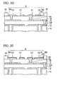
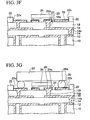
- FIGS.3A to 3H are sectional views showing a method of manufacturing an electronic parts built-in substrate according to an embodiment of the present invention in order.
- a base substrate 10 is prepared to manufacture a build-up wiring substrate.
- This base substrate 10 is made of insulating material such as glass epoxy resin, or the like.
- Through holes 10a are provided in the base substrate 10, then a through-hole plating layer 10b connected to a first wiring pattern 12 on the base substrate 10 respectively is formed on inner surfaces of the through holes 10a, and then the openings are buried with a resin body 10c.
- a first interlayer insulating film 14 is formed on the first wiring patterns 12.
- a resin such as epoxy resin, polyimide resin, polyphenylene ether resin, or the like may be employed.
- a resin film is formed by laminating a resin film on the first wiring patterns 12 and then thermally treating the film at 80 to 140 °C to cure.
- the resin film may be formed by the spin coating method or the printing.
- first interlayer insulating film 14 on the first wiring patterns 12 are worked by the laser or the RIE.
- first via holes 14x each having a depth that reaches the first wiring pattern 12 are formed.
- second wiring patterns 16 connected to the first wiring patterns 12 via the first via holes 14x are formed on the first interlayer insulating film 14 by the semi-additive process.
- a seed Cu layer (not shown) is formed on inner surfaces of the first via holes 14x and the first interlayer insulating film 14 by the electroless plating or the sputter method, and then a resist film (not shown) having opening portions that correspond to the second wiring patterns 16 is formed. Then, Cu film patterns (not shown) are formed in the opening portions in the resist film by the electrolytic plating using the seed Cu layer as a plating power-supply layer. Then, the resist film is removed and then the seed Cu film is etched while using the Cu film patterns as a mask. In this case, the subtractive process or the full additive process may be used in place of the semi-additive process.
- a second interlayer insulating film 18 made of the same material as the first interlayer insulating film 14 is formed on the second wiring patterns 16, and then second via holes 18x are formed in predetermined portions of the second interlayer insulating film 18 on the second wiring patterns 16.
- third wiring patterns 20 connected to the second wiring patterns 16 via the second via holes 18x are formed on the second interlayer insulating film 18 by the same method as the method of forming the second wiring patterns 16.
- the third wiring patterns 20 are formed in a state that a first connecting pad C1 to which the bump of the first semiconductor chip is connected later and a second connecting pad C2 to which the bump of the second semiconductor chip is connected are provided thereto.
- solder resist film 22 (protection insulating film) having an opening portion 22x to expose collectively the packaging area A, in which a plurality of first, second connecting pads C1, C2 of the third wiring patterns 20 are arranged, is formed. That is, the solder resist film 22 is formed to surround the packaging area A.
- an Ni (nickel)/Au (gold) layer 21 is formed on the third wiring patterns 20 containing the first, second connecting pads C1, C2, which are exposed from the packaging area A, by the electroless plating while using the solder resist film 22 as a mask.
- a first semiconductor chip 24 (first electronic parts) having bumps 24a is prepared.
- This semiconductor chip 24 is obtained by grinding a semiconductor wafer (not shown) having elements such as transistors, etc. and connecting terminals on the element forming surface side to reduce a thickness and then dicing the semiconductor wafer into individual pieces.
- the semiconductor chip 24 (except the bumps 24a) is reduced in thickness up to 150 ⁇ m or less, preferably 10 to 100 ⁇ m.
- the bumps 24a of the first semiconductor chip 24 are formed on the connecting terminals of the semiconductor chip 24, before or after the semiconductor wafer is subjected to the dicing.
- the bumps 24a of the first semiconductor chip 24 are flip-chip connected to the Ni/Au layers 21 on the first connecting pads C1 of the third wiring patterns 20 (FIG.3E).
- the Au bump, the solder bump, or the like may be used as the bumps 24a of the first semiconductor chip 24.
- Au bump When the Au bump is used, Au and Au are bonded by the ultrasonic wave. Also, when the solder bump is used, the solder and Au are bonded by the reflow heating.
- a second semiconductor chip 26 (second electronic parts) having bumps 26a and having an area that is larger than an area of the first semiconductor chip 24 is prepared.
- the bumps 26a of the second semiconductor chip 26 are flip-chip connected to the Ni/Au layers 21 on the second connecting pads C2 of the third wiring patterns 20 (FIG.3E) arranged on the outside of the periphery of the first semiconductor chip 24. Accordingly, the second semiconductor chip 26 is packaged at a predetermined interval from the upper surface of the first semiconductor chip 24, and the first semiconductor chip 24 is installed into a space between the lower surface of the second semiconductor chip 26 and the wiring substrate.
- a height of the bumps 26a of the second semiconductor chip 26 is set higher than a thickness containing the bumps 24a of the first semiconductor chip 24.
- a height of the bumps 26a of the second semiconductor chip 26 is set to about 100 ⁇ m when a thickness of the first semiconductor chip 24 is about 50 ⁇ m and a height of the bumps 24a is about 20 ⁇ m.
- the semiconductor chip is taken as an example of the electronic parts. But various electronic parts such as the capacitor parts, or the like may be employed.
- a filling insulating body 28 is formed by filling the underfill resin in the clearance under the first semiconductor chip 24, the clearances on both surface sides of the first semiconductor chip 24, the clearance between the upper surface of the first semiconductor chip 24 and the lower surface of the second semiconductor chip 26, and the clearances between the side surfaces of the second semiconductor chip 26 and the opening portion 22x of the solder resist film 22 and then thermally treating the resin to cure.
- the first semiconductor chip 24 is buried in the filling insulating body 28 but also the clearances under the second semiconductor chip 26 and on the side surface side thereof are filled with the filling insulating body 28.
- the filling insulating body 28 on the side surface side of the second semiconductor chip 26 is formed in a state that such body is dammed up by the side surface of the opening portion 22x of the solder resist film 22.
- the resin which contains filler (silica), and has a coefficient of thermal expansion (CTE) of 20 to 30 ppm/°C and has a Young's modulus of 10 to 15 GPa is used.
- the first semiconductor chip 24 is mounted on the wiring substrate in a state that such first semiconductor chip 24 is buried in the filling insulating body 28, and the second semiconductor chip 26 is mounted on the wiring substrate in a state that such second semiconductor chip 26 is stacked three-dimensionally over the first semiconductor chip 24.
- the solder resist film 22 having the opening portion 22x to expose collectively the packaging area A in which a plurality of first, second connecting pads C1, C2 are arranged is formed.
- a desired bonding area can be assured upon bonding the bumps 24a, 26a of the semiconductor chips 24, 26 to the connecting pads C1, C2 and thus the reliability of the electrical bonding can be improved, even though a pitch between the connecting pads C1, C2 is narrowed (e.g., about 150 ⁇ m or less).
- the opening portions in the solder resist film are liable to displace from the major portions of the connecting pads C1, C2 in formation due to displacements in the forming step when a pitch between the connecting pads C1, C2 is narrowed. Therefore, the bonding area between the bumps of the semiconductor chip and the connecting pads C1, C2 is reduced and the bonding failure, and the like are readily caused with the reduction in a bonding strength of the bumps.
- the first to third wiring patterns 12, 16, 20 are formed on the base substrate 10 in a multi-layered fashion, and then these wiring patterns 12, 16, 20 are connected mutually via the first and second via holes 14x, 18x provided in the first and second interlayer insulating films 14, 18.
- the third wiring patterns 20 have a plurality of connecting pads C1, C2, and the solder resist film 22 having the opening portion 22x to expose collectively the packaging area A in which the first, second connecting pads C1, C2 are arranged is formed on the second interlayer insulating film 18.
- the bumps 24a of the first semiconductor chip 24 are flip-chip connected to the Ni/Au layers 21 on the first connecting pads C1 of the third wiring patterns 20.
- the bumps 26a of the second semiconductor chip 26, which have a larger area than an area of the first semiconductor chip 24, are flip-chip connected to the Ni/Au layers 21 on the second connecting pads C2 arranged on the outside of the periphery of the first semiconductor chip 24. Then, a height of the bumps 26a of the second semiconductor chip 26 is set higher than a thickness containing the bumps 24a of the first semiconductor chip 24, whereby the first semiconductor chip 24 is installed into an area between the lower surface of the second semiconductor chip 26 and the wiring substrate.
- the filling insulating body 28 is filled in the clearances under the first semiconductor chip 24 and the second semiconductor chip 26 and on the side surface sides thereof, and the first semiconductor chip 24 is mounted to be buried in the filling insulating body 28.
- the first semiconductor chip 24 is buried in the filling insulating body 28 made of the underfill resin for which the material having a high crack resistance can be easily chosen. For this reason, no crack is generated in the filling insulating body 28 on the peripheral portion of the first semiconductor chip 24 during the temperature cycle test, and thus the reliability of the electronic parts built-in substrate 1 can be improved.
- the special steps such as the step of patterning the insulating film having the opening portion in the packaging area, the step of forming the flat interlayer insulating film by filling the insulating film in the clearances between the electronic parts packaged in the packaging area and the insulating film, etc. are required.
- the first and second semiconductor chips 24, 26 are flip-chip connected in sequence to the wiring substrates manufactured by the normal manufacturing method such that the first semiconductor chip 24 is installed in the space under the second semiconductor chip 26, and then the filling insulating body 28 is filled at a time in the clearances under the first and second semiconductor chips 24, 26. Therefore, the electronic parts built-in substrate 1 of the present embodiment can be manufactured by very simple manufacturing steps and at a low cost rather than the related arts 1 and 2.
- the film thickness of the insulating film of the wiring substrate should be formed to coincide with the thickness of the semiconductor chip. Therefore, since the film thickness of the insulating film can be adjusted appropriately to meet the characteristics of the wiring substrate, an overall thickness of the electronic parts built-in substrate can be adjusted thinly rather than the related arts 1 and 2.
- the substrate in which three wiring patterns are stacked on the base substrate is exemplified as the wiring substrate.
- various wiring substrates in which the wiring patterns are provided in the n-layered (n is an integer of 1 or more) fashion may be employed.
- a mode in which the n-layered (n is an integer of 1 or more) wiring pattern is also formed on the back surface side of the base substrate 10 may be employed.
Landscapes
- Engineering & Computer Science (AREA)
- Microelectronics & Electronic Packaging (AREA)
- Manufacturing & Machinery (AREA)
- Production Of Multi-Layered Print Wiring Board (AREA)
- Structures For Mounting Electric Components On Printed Circuit Boards (AREA)
- Wire Bonding (AREA)
Abstract
Description
- The present invention relates to an electronic parts built-in substrate and, more particularly, an electronic parts built-in substrate having a structure in which electronic parts are packaged in a multi-layered fashion in a state that these electronic parts are buried in insulating films and a method of manufacturing the same.
- The development of LSI technology serving as a key technology to implement multimedia devices is proceeding steadily to a higher speed and a larger capacity in data transmission. With this development, a higher density in the packaging technology serving as the interface between LSI and an electronic device is advanced.
- In reply to the request for the higher density, an electronic parts built-in substrate having the structure in which electronic parts are packaged on a wiring substrate in a multi-layered fashion in a state that semiconductor chips are buried in an insulating film was developed. As an example, in Patent Literature 1 (Patent Application Publication (KOKAI) Hei 11-274734), it is set forth that a multi-layered wiring structure is formed by flip-chip connecting a bare chip on the wiring substrate, then forming an insulating film on the bare chip, then forming wiring patterns on the insulating film, and then repeating these steps plural times.
- Meanwhile, in the production of the above electronic parts built-in substrate, upon forming the insulating film on the semiconductor chip, such insulating film is formed in the situation that a level difference is caused due to a thickness of the semiconductor chip. If the level difference is caused in the insulating film on the semiconductor chip, defocus is liable to occur in the photolithography applied to form the wiring patterns on the insulating film. Thus, it becomes difficult to form the wiring patterns on the insulating film with good precision.
- Further, since a level difference is also caused in the wiring patterns formed on the insulating film, there is a possibility of lowering the reliability of the electrical bonding applied to flip-chip bond the upper semiconductor chip to the wiring patterns.
- Therefore, a technology capable of forming easily a flat insulating film on the semiconductor chip is desired.
- Accordingly, it is desirable to provide an electronic parts built-in substrate in which electronic parts are buried in insulating films and packaged at low cost with good reliability to cause no disadvantage, and a method of manufacturing the same.
- According to an electronic parts built-in substrate embodying the present invention, there is provided a wiring substrate including a wiring pattern having connecting pads; a first electronic parts, a bump of which is flip-chip connected to the connecting pad; a second electronic parts, a bump of which is flip-chip connected to the connecting pad arranged on an outside of a periphery of the first electronic parts and which is packaged at a predetermined interval from an upper surface of the first electronic parts; and a filling insulating body filled in a clearance between the first electronic parts and the wiring substrate and clearances between the second electronic parts and the first electronic parts and the wiring substrate; wherein the first electronic parts is buried in the filling insulating body.
- In an electronic parts built-in substrate embodying the present invention, first the bumps of the first electronic parts (the thinned semiconductor chip, or the like) are flip-chip connected to the connecting pads of the wiring substrate that includes the wiring patterns having the connecting pads. Then, the bumps of the second electronic parts (the semiconductor chip, or the like) having a larger area than an area of the first electronic parts are flip-chip connected to the connecting pads arranged on the outside of the periphery of the first electronic parts. That is, a height of the bumps of the second electronic parts is set higher than a thickness that contains the bumps of the first electronic parts, and the second electronic parts is packaged on the wiring substrate at a predetermined interval from the upper surface of the first electronic parts, and the first electronic parts is installed in a space between the lower surface of the second electronic parts and the wiring substrate.
- Then, the filling insulating body (the underfill resin) is filled in the clearance between the first electronic parts and the wiring substrate and clearances between the second electronic parts and the first electronic parts and the wiring substrate, and thus the first electronic parts is buried in the filling insulating body.
- In the
related arts related arts related arts - In contrast, in an embodiment of the present invention, the first and second semiconductor chips are flip-chip connected in sequence to the wiring substrates manufactured by the normal manufacturing method such that the first semiconductor chip is installed in the space under the second semiconductor chip, and then the filling insulating body (underfill resin) is filled at a time in the clearances under the first and second semiconductor chips. Therefore, the first semiconductor chip is easily buried in the filling insulating body (underfill resin) having the high crack resistance and then packaged.
- As a result, the manufacturing steps become very simple rather than the
related arts - Also, unlike the
related arts - Reference will now be made, by way of example, to the accompanying drawings, in which:
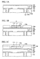
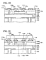
- FIGS.1A to 1E are sectional views showing a
method of manufacturing an electronic parts built-in
substrate according to the
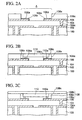
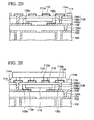
related art 1; - FIGS.2A to 2E are sectional views showing a
method of manufacturing an electronic parts built-in
substrate according to the
related art 2; and - FIGS.3A to 3H are sectional views showing a method of manufacturing an electronic parts built-in substrate according to an embodiment of the present invention.
-
- An embodiment of the present invention will be explained with reference to the drawings hereinafter.
- The related arts having relevance to the present invention and their disadvantages will be explained prior to explanation of an embodiment of the present invention.
- In the method of manufacturing the electronic parts built-in substrate according to the
related art 1, as shown in FIG.1A, first aninsulating base substrate 100, to manufacture a built-up wiring substrate, is prepared. Throughholes 100x are provided in thebase substrate 100, then through-hole plating layers 102x connected tofirst wiring patterns 102 are formed on inner surfaces of the throughholes 100x, and then the openings are buried with aresin body 101. - Then, a first
interlayer insulating film 104 made of resin to coat thefirst wiring patterns 102 is formed. Then, predetermined portions of the firstinterlayer insulating film 104 on thefirst wiring patterns 102 are worked by the laser or the RIE. Thus, first viaholes 104x each having a depth that reaches thefirst wiring pattern 102 are formed. Then, asecond wiring pattern 106 connected to thefirst wiring patterns 102 via thefirst via holes 104x is formed on the first interlayerinsulating film 104. - Then, as shown in FIG.1B, a first
insulating film 108a having anopening portion 108x in a packaging area A, in which the semiconductor chip is flip-chip mounted, of thesecond wiring pattern 106 and the first interlayerinsulating film 104 is formed. - Then, a
semiconductor chip 110 which hasconnection terminals 110a and whose thickness is thinned up to about 150 µm or less is prepared. Then, a back surface of thesemiconductor chip 110 is secured onto thewiring pattern 106 via anadhesive layer 111 such that theconnection terminals 110a of thesemiconductor chip 110 are directed upward. At this time, since the firstinsulating film 108a is formed in areas except the packaging area A to have a film thickness almost equal to a thickness of thesemiconductor chip 110, an upper surface of thesemiconductor chip 110 and an upper surface of the firstinsulating film 108a have an almost same height respectively and therefore the level difference caused by thesemiconductor chip 110 is overcome. - Then, as shown in FIG.1C, a second
insulating film 108b is formed by pasting a resin film on thesemiconductor chip 110 and the firstinsulating film 108a. At this time, the secondinsulating film 108b is filled in clearances between side surfaces of thesemiconductor chip 110 and side surfaces of theopening portion 108x in the firstinsulating film 108a to form a coplanar upper surface. - In this manner, a second
interlayer insulating film 108 consisting of the firstinsulating film 108a and the secondinsulating film 108b is obtained. Thus, the structure in which thesemiconductor chip 110 is face-up buried in the flat secondinterlayer insulating film 108 and packaged is obtained. - Then, as shown in FIG.1D,
second via holes 108y are formed in predetermined portions in the secondinterlayer insulating film 108 on theconnection terminals 110a of thesemiconductor chip 110 and thesecond wiring pattern 106. Then,third wiring patterns 112 connected to theconnection terminals 110a of thesemiconductor chip 110 and thesecond wiring pattern 106 via thesecond via holes 108y respectively are formed on the second interlayerinsulating film 108. - Then, a
solder resist film 114 having anopening portion 114x to expose predetermined portions of thethird wiring patterns 112 is formed on the second interlayerinsulating film 108. Then, Ni/Au layers 112a are formed on thethird wiring patterns 112 in theopening portion 114x by the electroless plating. - Then, as shown in FIG.1E,
bumps 116a of anupper semiconductor chip 116 with thebumps 116a are flip-chip connected to the Ni/Au plating layers 112a on thethird wiring patterns 112. Then, anunderfill resin 118 is filled in clearances under theupper semiconductor chip 116. With the above, the electronic parts built-in substrate of therelated art 1 can be obtained. - In the electronic parts built-in substrate of the
related art 1, the level difference caused due to thesemiconductor chip 110 when thesemiconductor chip 110 is buried in the second interlayerinsulating film 108 can be easily eliminated, nevertheless a crack is prone to occur in portions of the second insulating film (resin film) 108b buried in the clearances on the outside of the periphery of the semiconductor chip 110 (in particular, the portions corresponding to the corner portions of the semiconductor chip) when the temperature cycle test is applied in the range of 125 to -55 °C. Therefore, the measure must be taken such that a special resin film having a high crack resistance should be used as the secondinsulating film 108b, and so forth, and it is possible that an increase in a production cost is brought about. - In the method of manufacturing the electronic parts built-in substrate according to the
related art 2, as shown in FIG.2A, first thebase substrate 100 having thefirst wiring patterns 102 is prepared, like therelated art 1. Then, thesecond wiring patterns 106 connected to thefirst wiring patterns 102 via thefirst via holes 104x formed in the first interlayerinsulating film 104 are formed on the first interlayerinsulating film 104. Then, the firstinsulating film 108a having theopening portion 108x in the packaging area A in which the semiconductor chip is mounted is formed. At this time, connectingpads 106x of thesecond wiring patterns 106, to which the semiconductor chip is flip-chip connected later, are exposed from the packaging area A. Then, Ni/Au layers 106a are formed on the connectingpads 106x of thesecond wiring patterns 106, which are exposed from the packaging area A, by the electroless plating. - Then, as shown in FIG.2B, the
semiconductor chip 110 which has thebumps 110a and whose thickness is thinned up to about 150 µm or less is prepared. Then, thebumps 110a of thesemiconductor chip 110 are flip-chip connected to the Ni/Au layers 106a on the connectingpads 106x of thesecond wiring patterns 106. Then, anunderfill resin 108c is filled in the clearances under thesemiconductor chip 110 and the clearances between the side surfaces of thesemiconductor chip 110 and the side surfaces of theopening portion 108x in the firstinsulating film 108a. Then, as shown in FIG.2C, the secondinsulating film 108b is formed on the upper surface of thesemiconductor chip 110. Thus, the secondinterlayer insulating film 108 consisting of the firstinsulating film 108a, the secondinsulating film 108b, and theunderfill resin 108c is obtained. - Then, as shown in FIG.2D, the
second via holes 108y are formed in the predetermined portions in the secondinterlayer insulating film 108 on thesecond wiring patterns 106. Then, thethird wiring patterns 112 connected to thesecond wiring patterns 106 via the second viaholes 108y are formed on the secondinterlayer insulating film 108. - Then, the solder resist
film 114 having the openingportion 114x to expose the predetermined portions of thethird wiring patterns 112 is formed on the secondinterlayer insulating film 108. Then, the Ni/Au layers 112a are formed on thethird wiring patterns 112, which are exposed from theopening portion 114x, by the electroless plating. - Then, as shown in FIG.2E, the
bumps 116a of anupper semiconductor chip 116 having thebumps 116a are flip-chip connected to the Ni/Au layers 112a on thethird wiring patterns 112. Then, theunderfill resin 118 is filled in the clearances under theupper semiconductor chip 116. With the above, the electronic parts built-in substrate of therelated art 2 can be obtained. - In the electronic parts built-in substrate of the
related art 2, like therelated art 1, the level difference caused due to thesemiconductor chip 110 whensuch semiconductor chip 110 is buried in the firstinterlayer insulating film 108 can be easily eliminated. However, in the step of filling theunderfill resin 108c in FIG.2B, it is difficult to control a supply amount of theunderfill resin 108c in such a way that the upper surface of theunderfill resin 108c and the upper surface of thesemiconductor chip 110 constitute a coplanar surface. Therefore, in many cases theunderfill resin 108c is formed to rise around the peripheral portion of thesemiconductor chip 110. As a result, a height of thethird wiring patterns 112 formed over this resin is varied and thus the reliability of the electrical bonding of theupper semiconductor chip 116 is lowered. - In this manner, according to the
related art 2, since the measure must be taken such that the planarizing step should be particularly added, etc., it is possible that an increase in a production cost is brought about. - An electronic parts built-in substrate according to an embodiment of the present invention to be explained in the following can overcome disadvantages of the above
related arts - FIGS.3A to 3H are sectional views showing a method of manufacturing an electronic parts built-in substrate according to an embodiment of the present invention in order. As shown in FIG.3A, first a
base substrate 10 is prepared to manufacture a build-up wiring substrate. Thisbase substrate 10 is made of insulating material such as glass epoxy resin, or the like. Throughholes 10a are provided in thebase substrate 10, then a through-hole plating layer 10b connected to afirst wiring pattern 12 on thebase substrate 10 respectively is formed on inner surfaces of the throughholes 10a, and then the openings are buried with aresin body 10c. - Then, as shown in FIG.3B, a first
interlayer insulating film 14 is formed on thefirst wiring patterns 12. As the firstinterlayer insulating film 14, a resin such as epoxy resin, polyimide resin, polyphenylene ether resin, or the like may be employed. As an example of the forming method, a resin film is formed by laminating a resin film on thefirst wiring patterns 12 and then thermally treating the film at 80 to 140 °C to cure. - Alternatively, the resin film may be formed by the spin coating method or the printing.
- Then, predetermined portions of the first
interlayer insulating film 14 on thefirst wiring patterns 12 are worked by the laser or the RIE. Thus, first viaholes 14x each having a depth that reaches thefirst wiring pattern 12 are formed. Then,second wiring patterns 16 connected to thefirst wiring patterns 12 via the first viaholes 14x are formed on the firstinterlayer insulating film 14 by the semi-additive process. - To explain in detail, a seed Cu layer (not shown) is formed on inner surfaces of the first via
holes 14x and the firstinterlayer insulating film 14 by the electroless plating or the sputter method, and then a resist film (not shown) having opening portions that correspond to thesecond wiring patterns 16 is formed. Then, Cu film patterns (not shown) are formed in the opening portions in the resist film by the electrolytic plating using the seed Cu layer as a plating power-supply layer. Then, the resist film is removed and then the seed Cu film is etched while using the Cu film patterns as a mask. In this case, the subtractive process or the full additive process may be used in place of the semi-additive process. - Then, as shown in FIG.3C, a second
interlayer insulating film 18 made of the same material as the firstinterlayer insulating film 14 is formed on thesecond wiring patterns 16, and then second viaholes 18x are formed in predetermined portions of the secondinterlayer insulating film 18 on thesecond wiring patterns 16. Then,third wiring patterns 20 connected to thesecond wiring patterns 16 via the second viaholes 18x are formed on the secondinterlayer insulating film 18 by the same method as the method of forming thesecond wiring patterns 16. - At this time, the
third wiring patterns 20 are formed in a state that a first connecting pad C1 to which the bump of the first semiconductor chip is connected later and a second connecting pad C2 to which the bump of the second semiconductor chip is connected are provided thereto. - Then, as shown in FIG.3D, a solder resist film 22 (protection insulating film) having an opening
portion 22x to expose collectively the packaging area A, in which a plurality of first, second connecting pads C1, C2 of thethird wiring patterns 20 are arranged, is formed. That is, the solder resistfilm 22 is formed to surround the packaging area A. - Then, as shown in FIG.3E, an Ni (nickel)/Au (gold)
layer 21 is formed on thethird wiring patterns 20 containing the first, second connecting pads C1, C2, which are exposed from the packaging area A, by the electroless plating while using the solder resistfilm 22 as a mask. - Then, as shown in FIG.3F, a first semiconductor chip 24 (first electronic parts) having
bumps 24a is prepared. Thissemiconductor chip 24 is obtained by grinding a semiconductor wafer (not shown) having elements such as transistors, etc. and connecting terminals on the element forming surface side to reduce a thickness and then dicing the semiconductor wafer into individual pieces. The semiconductor chip 24 (except thebumps 24a) is reduced in thickness up to 150 µm or less, preferably 10 to 100 µm. Thebumps 24a of thefirst semiconductor chip 24 are formed on the connecting terminals of thesemiconductor chip 24, before or after the semiconductor wafer is subjected to the dicing. - Then, the
bumps 24a of thefirst semiconductor chip 24 are flip-chip connected to the Ni/Au layers 21 on the first connecting pads C1 of the third wiring patterns 20 (FIG.3E). As thebumps 24a of thefirst semiconductor chip 24, the Au bump, the solder bump, or the like may be used. When the Au bump is used, Au and Au are bonded by the ultrasonic wave. Also, when the solder bump is used, the solder and Au are bonded by the reflow heating. - Then, as shown in FIG.3G, a second semiconductor chip 26 (second electronic parts) having
bumps 26a and having an area that is larger than an area of thefirst semiconductor chip 24 is prepared. Thebumps 26a of thesecond semiconductor chip 26 are flip-chip connected to the Ni/Au layers 21 on the second connecting pads C2 of the third wiring patterns 20 (FIG.3E) arranged on the outside of the periphery of thefirst semiconductor chip 24. Accordingly, thesecond semiconductor chip 26 is packaged at a predetermined interval from the upper surface of thefirst semiconductor chip 24, and thefirst semiconductor chip 24 is installed into a space between the lower surface of thesecond semiconductor chip 26 and the wiring substrate. - As a consequence, a height of the
bumps 26a of thesecond semiconductor chip 26 is set higher than a thickness containing thebumps 24a of thefirst semiconductor chip 24. As an example of this, a height of thebumps 26a of thesecond semiconductor chip 26 is set to about 100 µm when a thickness of thefirst semiconductor chip 24 is about 50 µm and a height of thebumps 24a is about 20 µm. - In this case, the semiconductor chip is taken as an example of the electronic parts. But various electronic parts such as the capacitor parts, or the like may be employed.
- Then, as shown in FIG.3H, a filling insulating
body 28 is formed by filling the underfill resin in the clearance under thefirst semiconductor chip 24, the clearances on both surface sides of thefirst semiconductor chip 24, the clearance between the upper surface of thefirst semiconductor chip 24 and the lower surface of thesecond semiconductor chip 26, and the clearances between the side surfaces of thesecond semiconductor chip 26 and the openingportion 22x of the solder resistfilm 22 and then thermally treating the resin to cure. Thus, not only thefirst semiconductor chip 24 is buried in the filling insulatingbody 28 but also the clearances under thesecond semiconductor chip 26 and on the side surface side thereof are filled with the filling insulatingbody 28. The filling insulatingbody 28 on the side surface side of thesecond semiconductor chip 26 is formed in a state that such body is dammed up by the side surface of the openingportion 22x of the solder resistfilm 22. - As the filling insulating
body 28, in order to improve the reliability such as the crack resistance, etc., it is preferable that the resin which contains filler (silica), and has a coefficient of thermal expansion (CTE) of 20 to 30 ppm/°C and has a Young's modulus of 10 to 15 GPa is used. - In this fashion, the
first semiconductor chip 24 is mounted on the wiring substrate in a state that suchfirst semiconductor chip 24 is buried in the filling insulatingbody 28, and thesecond semiconductor chip 26 is mounted on the wiring substrate in a state that suchsecond semiconductor chip 26 is stacked three-dimensionally over thefirst semiconductor chip 24. - With the above, an electronic parts built-in
substrate 1 of the present embodiment is completed. - In this case, as described above, in the present embodiment, in order to bury the
first semiconductor chip 24 in the filling insulatingbody 28, the solder resistfilm 22 having the openingportion 22x to expose collectively the packaging area A in which a plurality of first, second connecting pads C1, C2 are arranged is formed. Such structure is also suitable from such a respect that a desired bonding area can be assured upon bonding thebumps - In other words, if the method of forming the continuous solder resist film having the opening portions that expose the major portions of the connecting pads C1, C2 of the
third wiring patterns 20 respectively is employed, the opening portions in the solder resist film are liable to displace from the major portions of the connecting pads C1, C2 in formation due to displacements in the forming step when a pitch between the connecting pads C1, C2 is narrowed. Therefore, the bonding area between the bumps of the semiconductor chip and the connecting pads C1, C2 is reduced and the bonding failure, and the like are readily caused with the reduction in a bonding strength of the bumps. - In the electronic parts built-in
substrate 1 of the present embodiment, the first tothird wiring patterns base substrate 10 in a multi-layered fashion, and then thesewiring patterns holes interlayer insulating films third wiring patterns 20 have a plurality of connecting pads C1, C2, and the solder resistfilm 22 having the openingportion 22x to expose collectively the packaging area A in which the first, second connecting pads C1, C2 are arranged is formed on the secondinterlayer insulating film 18. Then, thebumps 24a of thefirst semiconductor chip 24 are flip-chip connected to the Ni/Au layers 21 on the first connecting pads C1 of thethird wiring patterns 20. - Also, the
bumps 26a of thesecond semiconductor chip 26, which have a larger area than an area of thefirst semiconductor chip 24, are flip-chip connected to the Ni/Au layers 21 on the second connecting pads C2 arranged on the outside of the periphery of thefirst semiconductor chip 24. Then, a height of thebumps 26a of thesecond semiconductor chip 26 is set higher than a thickness containing thebumps 24a of thefirst semiconductor chip 24, whereby thefirst semiconductor chip 24 is installed into an area between the lower surface of thesecond semiconductor chip 26 and the wiring substrate. - In addition, the filling insulating
body 28 is filled in the clearances under thefirst semiconductor chip 24 and thesecond semiconductor chip 26 and on the side surface sides thereof, and thefirst semiconductor chip 24 is mounted to be buried in the filling insulatingbody 28. - In this manner, in the present embodiment, the
first semiconductor chip 24 is buried in the filling insulatingbody 28 made of the underfill resin for which the material having a high crack resistance can be easily chosen. For this reason, no crack is generated in the filling insulatingbody 28 on the peripheral portion of thefirst semiconductor chip 24 during the temperature cycle test, and thus the reliability of the electronic parts built-insubstrate 1 can be improved. - Also, in the
related arts first semiconductor chip 24, the special steps such as the step of patterning the insulating film having the opening portion in the packaging area, the step of forming the flat interlayer insulating film by filling the insulating film in the clearances between the electronic parts packaged in the packaging area and the insulating film, etc. are required. - In contrast, in the present embodiment, the first and second semiconductor chips 24, 26 are flip-chip connected in sequence to the wiring substrates manufactured by the normal manufacturing method such that the
first semiconductor chip 24 is installed in the space under thesecond semiconductor chip 26, and then the filling insulatingbody 28 is filled at a time in the clearances under the first and second semiconductor chips 24, 26. Therefore, the electronic parts built-insubstrate 1 of the present embodiment can be manufactured by very simple manufacturing steps and at a low cost rather than therelated arts - Also, unlike the
related art 2, since there is no necessity to consider the flatness in forming the filling insulatingbody 28, there is no necessity to control finely a supply amount of the underfill resin. - Further, unlike the
related arts related arts - In this case, in the present embodiment, the substrate in which three wiring patterns are stacked on the base substrate is exemplified as the wiring substrate. But various wiring substrates in which the wiring patterns are provided in the n-layered (n is an integer of 1 or more) fashion may be employed. Also, a mode in which the n-layered (n is an integer of 1 or more) wiring pattern is also formed on the back surface side of the
base substrate 10 may be employed.
Claims (12)
- An electronic parts built-in substrate comprising:wherein the first electronic parts (24) is buried in the filling insulating body (28).a wiring substrate (10) including a wiring pattern (20) having connecting pads (C1, C2);a first electronic parts (24), a bump (24a) of which is flip-chip connected to the connecting pad (C1);a second electronic parts (26), a bump (26a) of which is flip-chip connected to the connecting pad (C2) arranged on an outside of a periphery of the first electronic parts (24) and which is packaged at a predetermined interval from an upper surface of the first electronic parts (24); anda filling insulating body (28) filled in a clearance between the first electronic parts (24) and the wiring substrate (10), and clearances between the second electronic parts (26) and, the first electronic parts (24)and the wiring substrate (10);
- An electronic parts built-in substrate according to claim 1, wherein a height of the bump (26a) of the second electronic parts (26) is set higher than a thickness that contains the bump (24a) of the first electronic parts (24).
- An electronic parts built-in substrate according to claim 1 or 2, wherein a thickness of the first electronic parts (24) except the bump (24a) is 150 µm or less.
- An electronic parts built-in substrate according to any preceding claim, wherein a protection insulating film (22) in which an opening portion (22x) to open collectively a packaging area in which the first and second electronic parts (24, 26) are packaged is provided is formed on the wiring substrate (10), and the filling insulating body (28) is formed to extend from a side surface of the second electronic parts (26) to a side surface of the opening portion (22x) of the protection insulating film (22).
- An electronic parts built-in substrate according to any preceding claim, wherein the filling insulating body (28) is formed of a resin containing a filler and having a coefficient of thermal expansion of 20 to 30 ppm/°C.
- An electronic parts built-in substrate according to any preceding claim, wherein electronic parts (24, 26) is a semiconductor chip.
- A method of manufacturing an electronic parts built-in substrate comprising the steps of:preparing a wiring substrate (10) including a wiring pattern (20) having connecting pads (C1, C2);flip-chip connecting a bump (24a) of a first electronic parts (24) to the connecting pad (C1);flip-chip connecting a bump (26a) of a second electronic parts (26) to the connecting pad (C2) arranged on an outside of a periphery of the first electronic parts (24) to package the second electronic parts (26) at a predetermined interval from an upper surface of the first electronic parts (24); andfilling a filling insulating body (28) in a clearance between the first electronic parts (24) and the wiring substrate (10) and clearances between the second electronic parts (26) and the first electronic parts (24) and the wiring substrate (10) to bury the first electronic parts (24) in the filling insulating body (28).
- A method of manufacturing an electronic parts built-in substrate according to claim 7, further comprising the step of:wherein the filling insulating body (28) is formed to extend from a side surface of the second electronic parts (26) to a side surface of the opening portion (22x) of the protection insulating film (22) in the step of filling the filling insulating body (28).forming a protection insulating film (22) having an opening portion (22x) that exposes collectively a plurality of connecting pads (C1, C2) on the wiring substrate (10), prior to the step of flip-chip connecting the bump (24a) of the first electronic parts (24) to the connecting pad (C1); and
- A method of manufacturing an electronic parts built-in substrate according to claim 7 or 8, wherein a height of the bump (26a) of the second electronic parts (26) is set higher than a thickness that contains the bump (24a) of the first electronic parts (24).
- A method of manufacturing an electronic parts built-in substrate according to any one of claims 7 to 9 wherein a thickness of the first electronic parts (24) except the bump (24a) is 150 µm or less.
- A method of manufacturing an electronic parts built-in substrate according to any one of claims 7 to 10, wherein the filling insulating body (28) is formed of a resin containing a filler and having a coefficient of thermal expansion of 20 to 30 ppm/°C.
- A method of manufacturing an electronic parts built-in substrate according to any one of claims 7 to 11, wherein the electronic parts (24, 26) is a semiconductor chip.
Applications Claiming Priority (2)
| Application Number | Priority Date | Filing Date | Title |
|---|---|---|---|
| JP2003337323 | 2003-09-29 | ||
| JP2003337323A JP4198566B2 (en) | 2003-09-29 | 2003-09-29 | Manufacturing method of electronic component built-in substrate |
Publications (2)
| Publication Number | Publication Date |
|---|---|
| EP1519415A2 true EP1519415A2 (en) | 2005-03-30 |
| EP1519415A3 EP1519415A3 (en) | 2008-04-09 |
Family
ID=34191565
Family Applications (1)
| Application Number | Title | Priority Date | Filing Date |
|---|---|---|---|
| EP04254934A Ceased EP1519415A3 (en) | 2003-09-29 | 2004-08-17 | Electronic parts built-in substrate and method of manufacturing the same |
Country Status (5)
| Country | Link |
|---|---|
| US (2) | US20050067715A1 (en) |
| EP (1) | EP1519415A3 (en) |
| JP (1) | JP4198566B2 (en) |
| KR (1) | KR20050031364A (en) |
| TW (1) | TW200515585A (en) |
Cited By (6)
| Publication number | Priority date | Publication date | Assignee | Title |
|---|---|---|---|---|
| EP1780790A3 (en) * | 2005-10-27 | 2010-01-20 | Shinko Electric Industries Co., Ltd. | Electronic part built-in substrate and manufacturing method therefor |
| US8659134B2 (en) | 2008-07-22 | 2014-02-25 | Ge Embedded Electronics Oy | Multi-chip package and manufacturing method |
| CN103745967A (en) * | 2013-12-05 | 2014-04-23 | 南通富士通微电子股份有限公司 | Lead frame and package structure |
| EP3035230A1 (en) | 2014-12-19 | 2016-06-22 | Cardlab ApS | A method and an assembly for generating a magnetic field |
| US10095968B2 (en) | 2014-12-19 | 2018-10-09 | Cardlabs Aps | Method and an assembly for generating a magnetic field and a method of manufacturing an assembly |
| US10558901B2 (en) | 2015-04-17 | 2020-02-11 | Cardlab Aps | Device for outputting a magnetic field and a method of outputting a magnetic field |
Families Citing this family (23)
| Publication number | Priority date | Publication date | Assignee | Title |
|---|---|---|---|---|
| US11842972B2 (en) | 2004-09-28 | 2023-12-12 | Rohm Co., Ltd. | Semiconductor device with a semiconductor chip connected in a flip chip manner |
| JP2006100385A (en) | 2004-09-28 | 2006-04-13 | Rohm Co Ltd | Semiconductor device |
| DE102004047753B4 (en) * | 2004-09-30 | 2009-01-02 | Advanced Micro Devices, Inc., Sunnyvale | Improved chip contacting arrangement for chip carriers for flip-chip applications |
| US20080157316A1 (en) * | 2007-01-03 | 2008-07-03 | Advanced Chip Engineering Technology Inc. | Multi-chips package and method of forming the same |
| KR100867150B1 (en) * | 2007-09-28 | 2008-11-06 | 삼성전기주식회사 | Embedded Circuit Board and Chip Capacitor with Chip Capacitor |
| JP5395360B2 (en) * | 2008-02-25 | 2014-01-22 | 新光電気工業株式会社 | Manufacturing method of electronic component built-in substrate |
| US8441804B2 (en) * | 2008-07-25 | 2013-05-14 | Infineon Technologies Ag | Semiconductor device and method of manufacturing a semiconductor device |
| US7989950B2 (en) * | 2008-08-14 | 2011-08-02 | Stats Chippac Ltd. | Integrated circuit packaging system having a cavity |
| US8823160B2 (en) * | 2008-08-22 | 2014-09-02 | Stats Chippac Ltd. | Integrated circuit package system having cavity |
| JP5279631B2 (en) * | 2009-06-23 | 2013-09-04 | 新光電気工業株式会社 | Electronic component built-in wiring board and method of manufacturing electronic component built-in wiring board |
| US8390083B2 (en) | 2009-09-04 | 2013-03-05 | Analog Devices, Inc. | System with recessed sensing or processing elements |
| KR20110105530A (en) * | 2010-03-19 | 2011-09-27 | 삼성전자주식회사 | Electronic device, package and package manufacturing method comprising same |
| JP5667381B2 (en) | 2010-06-01 | 2015-02-12 | ピーエスフォー ルクスコ エスエイアールエルPS4 Luxco S.a.r.l. | Semiconductor device and manufacturing method thereof |
| US9407997B2 (en) | 2010-10-12 | 2016-08-02 | Invensense, Inc. | Microphone package with embedded ASIC |
| US9337116B2 (en) * | 2010-10-28 | 2016-05-10 | Stats Chippac, Ltd. | Semiconductor device and method of forming stepped interposer for stacking and electrically connecting semiconductor die |
| KR101301424B1 (en) * | 2011-11-28 | 2013-08-28 | 삼성전기주식회사 | Printed circuit board and method of manufacturing the same |
| KR101420514B1 (en) | 2012-10-23 | 2014-07-17 | 삼성전기주식회사 | Substrate structure having electronic components and method of manufacturing substrate structure having electronic components |
| CN104576883B (en) | 2013-10-29 | 2018-11-16 | 普因特工程有限公司 | Chip installation array substrate and its manufacturing method |
| JP6316609B2 (en) * | 2014-02-05 | 2018-04-25 | 新光電気工業株式会社 | WIRING BOARD, SEMICONDUCTOR DEVICE, WIRING BOARD MANUFACTURING METHOD, AND SEMICONDUCTOR DEVICE MANUFACTURING METHOD |
| US9653322B2 (en) * | 2014-06-23 | 2017-05-16 | Infineon Technologies Austria Ag | Method for fabricating a semiconductor package |
| US9666558B2 (en) | 2015-06-29 | 2017-05-30 | Point Engineering Co., Ltd. | Substrate for mounting a chip and chip package using the substrate |
| KR102494332B1 (en) * | 2015-07-15 | 2023-02-02 | 삼성전기주식회사 | Electronic Component Package |
| WO2022261913A1 (en) * | 2021-06-17 | 2022-12-22 | 庆鼎精密电子(淮安)有限公司 | Circuit board assembly and manufacturing method for circuit board assembly |
Citations (4)
| Publication number | Priority date | Publication date | Assignee | Title |
|---|---|---|---|---|
| EP1162867A1 (en) * | 1999-10-26 | 2001-12-12 | Ibiden Co., Ltd. | Multilayer printed wiring board and method of producing multilayer printed wiring board |
| US6339254B1 (en) | 1998-09-01 | 2002-01-15 | Texas Instruments Incorporated | Stacked flip-chip integrated circuit assemblage |
| US6369448B1 (en) | 2000-01-21 | 2002-04-09 | Lsi Logic Corporation | Vertically integrated flip chip semiconductor package |
| US6368895B1 (en) | 1998-01-20 | 2002-04-09 | Murata Manufacturing Co., Ltd. | Method of producing an electronic circuit device |
Family Cites Families (6)
| Publication number | Priority date | Publication date | Assignee | Title |
|---|---|---|---|---|
| TW373308B (en) * | 1995-02-24 | 1999-11-01 | Agere Systems Inc | Thin packaging of multi-chip modules with enhanced thermal/power management |
| JPH1084076A (en) * | 1996-09-05 | 1998-03-31 | Hitachi Ltd | Semiconductor device and manufacturing method thereof |
| US6335571B1 (en) * | 1997-07-21 | 2002-01-01 | Miguel Albert Capote | Semiconductor flip-chip package and method for the fabrication thereof |
| JPH11274734A (en) | 1998-03-20 | 1999-10-08 | Sony Corp | Electronic circuit device and method of manufacturing the same |
| TW533758B (en) * | 2000-07-31 | 2003-05-21 | Ngk Spark Plug Co | Printed wiring substrate and method for manufacturing the same |
| US6659512B1 (en) * | 2002-07-18 | 2003-12-09 | Hewlett-Packard Development Company, L.P. | Integrated circuit package employing flip-chip technology and method of assembly |
-
2003
- 2003-09-29 JP JP2003337323A patent/JP4198566B2/en not_active Expired - Fee Related
-
2004
- 2004-08-16 US US10/918,348 patent/US20050067715A1/en not_active Abandoned
- 2004-08-17 KR KR1020040064544A patent/KR20050031364A/en not_active Ceased
- 2004-08-17 EP EP04254934A patent/EP1519415A3/en not_active Ceased
- 2004-08-27 TW TW093125809A patent/TW200515585A/en unknown
-
2005
- 2005-02-04 US US11/049,958 patent/US7198986B2/en not_active Expired - Lifetime
Patent Citations (4)
| Publication number | Priority date | Publication date | Assignee | Title |
|---|---|---|---|---|
| US6368895B1 (en) | 1998-01-20 | 2002-04-09 | Murata Manufacturing Co., Ltd. | Method of producing an electronic circuit device |
| US6339254B1 (en) | 1998-09-01 | 2002-01-15 | Texas Instruments Incorporated | Stacked flip-chip integrated circuit assemblage |
| EP1162867A1 (en) * | 1999-10-26 | 2001-12-12 | Ibiden Co., Ltd. | Multilayer printed wiring board and method of producing multilayer printed wiring board |
| US6369448B1 (en) | 2000-01-21 | 2002-04-09 | Lsi Logic Corporation | Vertically integrated flip chip semiconductor package |
Cited By (8)
| Publication number | Priority date | Publication date | Assignee | Title |
|---|---|---|---|---|
| EP1780790A3 (en) * | 2005-10-27 | 2010-01-20 | Shinko Electric Industries Co., Ltd. | Electronic part built-in substrate and manufacturing method therefor |
| US8659134B2 (en) | 2008-07-22 | 2014-02-25 | Ge Embedded Electronics Oy | Multi-chip package and manufacturing method |
| US9691724B2 (en) | 2008-07-22 | 2017-06-27 | Ge Embedded Electronics Oy | Multi-chip package and manufacturing method |
| CN103745967A (en) * | 2013-12-05 | 2014-04-23 | 南通富士通微电子股份有限公司 | Lead frame and package structure |
| EP3035230A1 (en) | 2014-12-19 | 2016-06-22 | Cardlab ApS | A method and an assembly for generating a magnetic field |
| US10095968B2 (en) | 2014-12-19 | 2018-10-09 | Cardlabs Aps | Method and an assembly for generating a magnetic field and a method of manufacturing an assembly |
| US10614351B2 (en) | 2014-12-19 | 2020-04-07 | Cardlab Aps | Method and an assembly for generating a magnetic field and a method of manufacturing an assembly |
| US10558901B2 (en) | 2015-04-17 | 2020-02-11 | Cardlab Aps | Device for outputting a magnetic field and a method of outputting a magnetic field |
Also Published As
| Publication number | Publication date |
|---|---|
| US20050067715A1 (en) | 2005-03-31 |
| JP2005108962A (en) | 2005-04-21 |
| KR20050031364A (en) | 2005-04-06 |
| EP1519415A3 (en) | 2008-04-09 |
| US20050130349A1 (en) | 2005-06-16 |
| TW200515585A (en) | 2005-05-01 |
| JP4198566B2 (en) | 2008-12-17 |
| US7198986B2 (en) | 2007-04-03 |
Similar Documents
| Publication | Publication Date | Title |
|---|---|---|
| US7198986B2 (en) | Electronic parts built-in substrate and method of manufacturing the same | |
| KR101041011B1 (en) | Electronic component mounting structure and manufacturing method | |
| US10212818B2 (en) | Methods and apparatus for a substrate core layer | |
| US7285862B2 (en) | Electronic parts packaging structure in which a semiconductor chip is mounted on a wiring substrate and buried in an insulation film | |
| TWI476888B (en) | Package substrate with embedded perforation interposer and preparation method thereof | |
| KR20060043810A (en) | Electronic component mounting structure and manufacturing method | |
| KR101003437B1 (en) | Electronic component mounting structure and manufacturing method | |
| TW202410352A (en) | Semiconductor package and methods of forming the same | |
| JP2004363566A (en) | Electronic component mounted body and method of manufacturing the same | |
| JP4927146B2 (en) | Manufacturing method of electronic component mounting structure | |
| CN113643986A (en) | Fabrication method of structure for improving interconnection precision between embedded silicon bridge and chip |
Legal Events
| Date | Code | Title | Description |
|---|---|---|---|
| PUAI | Public reference made under article 153(3) epc to a published international application that has entered the european phase |
Free format text: ORIGINAL CODE: 0009012 |
|
| AK | Designated contracting states |
Kind code of ref document: A2 Designated state(s): AT BE BG CH CY CZ DE DK EE ES FI FR GB GR HU IE IT LI LU MC NL PL PT RO SE SI SK TR |
|
| AX | Request for extension of the european patent |
Extension state: AL HR LT LV MK |
|
| PUAL | Search report despatched |
Free format text: ORIGINAL CODE: 0009013 |
|
| AK | Designated contracting states |
Kind code of ref document: A3 Designated state(s): AT BE BG CH CY CZ DE DK EE ES FI FR GB GR HU IE IT LI LU MC NL PL PT RO SE SI SK TR |
|
| AX | Request for extension of the european patent |
Extension state: AL HR LT LV MK |
|
| RIC1 | Information provided on ipc code assigned before grant |
Ipc: H01L 21/56 20060101ALI20080229BHEP Ipc: H01L 25/065 20060101AFI20080229BHEP |
|
| 17P | Request for examination filed |
Effective date: 20081006 |
|
| 17Q | First examination report despatched |
Effective date: 20081107 |
|
| AKX | Designation fees paid |
Designated state(s): DE FI FR |
|
| STAA | Information on the status of an ep patent application or granted ep patent |
Free format text: STATUS: THE APPLICATION HAS BEEN REFUSED |
|
| 18R | Application refused |
Effective date: 20110913 |