EP1519413A1 - Via placement for layer transitions in flexible circuits with high density ball grid arrays - Google Patents
Via placement for layer transitions in flexible circuits with high density ball grid arrays Download PDFInfo
- Publication number
- EP1519413A1 EP1519413A1 EP04010830A EP04010830A EP1519413A1 EP 1519413 A1 EP1519413 A1 EP 1519413A1 EP 04010830 A EP04010830 A EP 04010830A EP 04010830 A EP04010830 A EP 04010830A EP 1519413 A1 EP1519413 A1 EP 1519413A1
- Authority
- EP
- European Patent Office
- Prior art keywords
- transmission line
- vias
- flexible circuit
- flex circuit
- electrical connection
- Prior art date
- Legal status (The legal status is an assumption and is not a legal conclusion. Google has not performed a legal analysis and makes no representation as to the accuracy of the status listed.)
- Withdrawn
Links
Images





Classifications
-
- H—ELECTRICITY
- H05—ELECTRIC TECHNIQUES NOT OTHERWISE PROVIDED FOR
- H05K—PRINTED CIRCUITS; CASINGS OR CONSTRUCTIONAL DETAILS OF ELECTRIC APPARATUS; MANUFACTURE OF ASSEMBLAGES OF ELECTRICAL COMPONENTS
- H05K1/00—Printed circuits
- H05K1/02—Details
- H05K1/11—Printed elements for providing electric connections to or between printed circuits
- H05K1/111—Pads for surface mounting, e.g. lay-out
- H05K1/112—Pads for surface mounting, e.g. lay-out directly combined with via connections
- H05K1/113—Via provided in pad; Pad over filled via
-
- H—ELECTRICITY
- H10—SEMICONDUCTOR DEVICES; ELECTRIC SOLID-STATE DEVICES NOT OTHERWISE PROVIDED FOR
- H10W—GENERIC PACKAGES, INTERCONNECTIONS, CONNECTORS OR OTHER CONSTRUCTIONAL DETAILS OF DEVICES COVERED BY CLASS H10
- H10W42/00—Arrangements for protection of devices
- H10W42/20—Arrangements for protection of devices protecting against electromagnetic or particle radiation, e.g. light, X-rays, gamma-rays or electrons
- H10W42/261—Arrangements for protection of devices protecting against electromagnetic or particle radiation, e.g. light, X-rays, gamma-rays or electrons characterised by their shapes or dispositions
- H10W42/267—Patterned shielding planes
-
- H—ELECTRICITY
- H10—SEMICONDUCTOR DEVICES; ELECTRIC SOLID-STATE DEVICES NOT OTHERWISE PROVIDED FOR
- H10W—GENERIC PACKAGES, INTERCONNECTIONS, CONNECTORS OR OTHER CONSTRUCTIONAL DETAILS OF DEVICES COVERED BY CLASS H10
- H10W70/00—Package substrates; Interposers; Redistribution layers [RDL]
- H10W70/60—Insulating or insulated package substrates; Interposers; Redistribution layers
- H10W70/62—Insulating or insulated package substrates; Interposers; Redistribution layers characterised by their interconnections
- H10W70/65—Shapes or dispositions of interconnections
-
- H—ELECTRICITY
- H10—SEMICONDUCTOR DEVICES; ELECTRIC SOLID-STATE DEVICES NOT OTHERWISE PROVIDED FOR
- H10W—GENERIC PACKAGES, INTERCONNECTIONS, CONNECTORS OR OTHER CONSTRUCTIONAL DETAILS OF DEVICES COVERED BY CLASS H10
- H10W70/00—Package substrates; Interposers; Redistribution layers [RDL]
- H10W70/60—Insulating or insulated package substrates; Interposers; Redistribution layers
- H10W70/67—Insulating or insulated package substrates; Interposers; Redistribution layers characterised by their insulating layers or insulating parts
- H10W70/688—Flexible insulating substrates
-
- H—ELECTRICITY
- H05—ELECTRIC TECHNIQUES NOT OTHERWISE PROVIDED FOR
- H05K—PRINTED CIRCUITS; CASINGS OR CONSTRUCTIONAL DETAILS OF ELECTRIC APPARATUS; MANUFACTURE OF ASSEMBLAGES OF ELECTRICAL COMPONENTS
- H05K1/00—Printed circuits
- H05K1/02—Details
- H05K1/0213—Electrical arrangements not otherwise provided for
- H05K1/0237—High frequency adaptations
-
- H—ELECTRICITY
- H05—ELECTRIC TECHNIQUES NOT OTHERWISE PROVIDED FOR
- H05K—PRINTED CIRCUITS; CASINGS OR CONSTRUCTIONAL DETAILS OF ELECTRIC APPARATUS; MANUFACTURE OF ASSEMBLAGES OF ELECTRICAL COMPONENTS
- H05K1/00—Printed circuits
- H05K1/18—Printed circuits structurally associated with non-printed electric components
- H05K1/189—Printed circuits structurally associated with non-printed electric components characterised by the use of flexible or folded printed circuits
-
- H—ELECTRICITY
- H05—ELECTRIC TECHNIQUES NOT OTHERWISE PROVIDED FOR
- H05K—PRINTED CIRCUITS; CASINGS OR CONSTRUCTIONAL DETAILS OF ELECTRIC APPARATUS; MANUFACTURE OF ASSEMBLAGES OF ELECTRICAL COMPONENTS
- H05K2201/00—Indexing scheme relating to printed circuits covered by H05K1/00
- H05K2201/09—Shape and layout
- H05K2201/09209—Shape and layout details of conductors
- H05K2201/09372—Pads and lands
- H05K2201/09381—Shape of non-curved single flat metallic pad, land or exposed part thereof; Shape of electrode of leadless component
-
- H—ELECTRICITY
- H05—ELECTRIC TECHNIQUES NOT OTHERWISE PROVIDED FOR
- H05K—PRINTED CIRCUITS; CASINGS OR CONSTRUCTIONAL DETAILS OF ELECTRIC APPARATUS; MANUFACTURE OF ASSEMBLAGES OF ELECTRICAL COMPONENTS
- H05K2201/00—Indexing scheme relating to printed circuits covered by H05K1/00
- H05K2201/10—Details of components or other objects attached to or integrated in a printed circuit board
- H05K2201/10613—Details of electrical connections of non-printed components, e.g. special leads
- H05K2201/10621—Components characterised by their electrical contacts
- H05K2201/10674—Flip chip
-
- H—ELECTRICITY
- H05—ELECTRIC TECHNIQUES NOT OTHERWISE PROVIDED FOR
- H05K—PRINTED CIRCUITS; CASINGS OR CONSTRUCTIONAL DETAILS OF ELECTRIC APPARATUS; MANUFACTURE OF ASSEMBLAGES OF ELECTRICAL COMPONENTS
- H05K2203/00—Indexing scheme relating to apparatus or processes for manufacturing printed circuits covered by H05K3/00
- H05K2203/04—Soldering or other types of metallurgic bonding
- H05K2203/049—Wire bonding
-
- H—ELECTRICITY
- H10—SEMICONDUCTOR DEVICES; ELECTRIC SOLID-STATE DEVICES NOT OTHERWISE PROVIDED FOR
- H10W—GENERIC PACKAGES, INTERCONNECTIONS, CONNECTORS OR OTHER CONSTRUCTIONAL DETAILS OF DEVICES COVERED BY CLASS H10
- H10W44/00—Electrical arrangements for controlling or matching impedance
- H10W44/20—Electrical arrangements for controlling or matching impedance at high-frequency [HF] or radio frequency [RF]
- H10W44/203—Electrical connections
- H10W44/216—Waveguides, e.g. strip lines
-
- H—ELECTRICITY
- H10—SEMICONDUCTOR DEVICES; ELECTRIC SOLID-STATE DEVICES NOT OTHERWISE PROVIDED FOR
- H10W—GENERIC PACKAGES, INTERCONNECTIONS, CONNECTORS OR OTHER CONSTRUCTIONAL DETAILS OF DEVICES COVERED BY CLASS H10
- H10W72/00—Interconnections or connectors in packages
- H10W72/071—Connecting or disconnecting
- H10W72/075—Connecting or disconnecting of bond wires
- H10W72/07531—Techniques
- H10W72/07532—Compression bonding, e.g. thermocompression bonding
- H10W72/07533—Ultrasonic bonding, e.g. thermosonic bonding
-
- H—ELECTRICITY
- H10—SEMICONDUCTOR DEVICES; ELECTRIC SOLID-STATE DEVICES NOT OTHERWISE PROVIDED FOR
- H10W—GENERIC PACKAGES, INTERCONNECTIONS, CONNECTORS OR OTHER CONSTRUCTIONAL DETAILS OF DEVICES COVERED BY CLASS H10
- H10W72/00—Interconnections or connectors in packages
- H10W72/071—Connecting or disconnecting
- H10W72/075—Connecting or disconnecting of bond wires
- H10W72/07551—Connecting or disconnecting of bond wires characterised by changes in properties of the bond wires during the connecting
- H10W72/07554—Connecting or disconnecting of bond wires characterised by changes in properties of the bond wires during the connecting changes in dispositions
-
- H—ELECTRICITY
- H10—SEMICONDUCTOR DEVICES; ELECTRIC SOLID-STATE DEVICES NOT OTHERWISE PROVIDED FOR
- H10W—GENERIC PACKAGES, INTERCONNECTIONS, CONNECTORS OR OTHER CONSTRUCTIONAL DETAILS OF DEVICES COVERED BY CLASS H10
- H10W72/00—Interconnections or connectors in packages
- H10W72/50—Bond wires
- H10W72/541—Dispositions of bond wires
- H10W72/5445—Dispositions of bond wires being orthogonal to a side surface of the chip, e.g. parallel arrangements
-
- H—ELECTRICITY
- H10—SEMICONDUCTOR DEVICES; ELECTRIC SOLID-STATE DEVICES NOT OTHERWISE PROVIDED FOR
- H10W—GENERIC PACKAGES, INTERCONNECTIONS, CONNECTORS OR OTHER CONSTRUCTIONAL DETAILS OF DEVICES COVERED BY CLASS H10
- H10W72/00—Interconnections or connectors in packages
- H10W72/50—Bond wires
- H10W72/541—Dispositions of bond wires
- H10W72/547—Dispositions of multiple bond wires
-
- H—ELECTRICITY
- H10—SEMICONDUCTOR DEVICES; ELECTRIC SOLID-STATE DEVICES NOT OTHERWISE PROVIDED FOR
- H10W—GENERIC PACKAGES, INTERCONNECTIONS, CONNECTORS OR OTHER CONSTRUCTIONAL DETAILS OF DEVICES COVERED BY CLASS H10
- H10W72/00—Interconnections or connectors in packages
- H10W72/50—Bond wires
- H10W72/551—Materials of bond wires
- H10W72/552—Materials of bond wires comprising metals or metalloids, e.g. silver
- H10W72/5522—Materials of bond wires comprising metals or metalloids, e.g. silver comprising gold [Au]
-
- H—ELECTRICITY
- H10—SEMICONDUCTOR DEVICES; ELECTRIC SOLID-STATE DEVICES NOT OTHERWISE PROVIDED FOR
- H10W—GENERIC PACKAGES, INTERCONNECTIONS, CONNECTORS OR OTHER CONSTRUCTIONAL DETAILS OF DEVICES COVERED BY CLASS H10
- H10W90/00—Package configurations
- H10W90/701—Package configurations characterised by the relative positions of pads or connectors relative to package parts
- H10W90/751—Package configurations characterised by the relative positions of pads or connectors relative to package parts of bond wires
- H10W90/754—Package configurations characterised by the relative positions of pads or connectors relative to package parts of bond wires between a chip and a stacked insulating package substrate, interposer or RDL
Definitions
- a flexible circuit is a type of electrical connection device that can be bent, twisted or wrapped to fit in extremely small spaces. Flex circuits are excellent for designs with fine line traces and high-density circuitry, and are more suited for dynamic applications and vibration conditions than are conventional printed wiring boards. Using flex circuits sometimes requires transferring an electrical signal from one side of the flex circuit to the opposing side of the flex circuit.
- Prior Art Figure 1A illustrates a side view of a flex circuit 110 comprising a first surface 240 and a second opposing surface 245.
- Flex circuit 110 has a transmission line 202 on surface 240 and a transmission line 204 on surface 245. It is appreciated that a conventional flexible circuit can have a plurality of transmission lines on each surface. Transmission lines 202 and 204 represent one of many transmission lines on each surface of the flex circuit 110.
- a high areal density connector scheme 120 is disposed on surface 240 and is electrically coupled to transmission line 202.
- Prior Art Figure 1B illustrates a top view of a portion of a ground plane 206 that is significantly discontinuous as a result of vias 246 disposed proximate connector scheme 120.
- the density of the connector scheme will result in overlapping ground relief holes, thus essentially removing the entire ground plane from the area under the BGA.
- placing vias proximate the BGA 120 introduces an additional element of discontinuity in the transmission path on the flex circuit 110.
- the vias are located throughout the flex circuit (i.e., not coincident connector scheme 120) to avoid the grounding problems associated with locating the vias near the high-density connector scheme.
- locating the vias throughout the flex circuit distributes electrical discontinuity throughout the entire flex circuit. Every discontinuity along a transmission line is a possible reflection, thus spreading discontinuities can possibly corrupt transmission of a signal along the entire flex circuit.
- a flexible electrical connector in accordance with the invention that transitions a signal from a transmission line on a first surface to a transmission line on an opposing surface while avoiding degradation of signal integrity.
- the flexible connector includes a flexible circuit having vias disposed in locations that reduce discontinuity in a ground plane separating transmission lines. By reducing the discontinuity of the ground plane separating the transmission lines, degradation of signal integrity in the flex circuit can be avoided. Furthermore, disposing vias at a location of electrical discontinuity combines discontinuity in the flex circuit, thus further avoiding degradation of signal integrity.
- Figure 1 A is a prior art side view illustration of a conventional two-layer flex circuit comprising vias located near a high areal density connector scheme for transitioning a signal from one side to the other side.
- Figure 1 B is a prior art top view illustration of the ground plane in the conventional two-layer flex circuit of prior art Figure 1A illustrating the discontinuity of the ground plane surrounding vias located near a high areal density connector scheme.
- Figure 2 is a side view illustration of an exemplary flexible circuit comprising vias located proximate a low areal density connector scheme in accordance with an embodiment of the invention.
- Figure 3 is a side view illustration of an exemplary flexible circuit assembly comprising vias proximate a low areal density connector scheme connecting an IC to the exemplary flex circuit in accordance with an embodiment of the invention.
- Figure 4A is a side view illustration of the exemplary flexible circuit in Figure 3 further comprising a heat sink in accordance with an embodiment of the invention.
- Figure 4B is a top view illustration of an exemplary flexible circuit comprising vias proximate a low-density connector scheme to provide for transferring a signal from a first side of the circuit to a second opposing side of the flex circuit in accordance with an embodiment of the invention.
- Figure 5A is a top view illustration of an exemplary flexible circuit comprising vias disposed linearly proximate a low areal density connector scheme to minimize discontinuity in a transmission path in accordance to an embodiment of the invention.
- Figure 5B is a perspective illustration of an exemplary flexible circuit having a via disposed proximate a teardrop shaped wirebond capture pad to minimize discontinuity in a ground plane in accordance with an embodiment of the invention.
- Figure 5C is a top view illustration of an exemplary flex circuit having a minimized discontinuity in a ground plane in accordance with an embodiment of the invention.
- FIG. 2 is a side-view illustration of an exemplary flexible circuit 300 having vias 455 disposed to reduce discontinuity in a ground plane 306 separating opposing transmission lines in accordance with embodiments of the invention.
- Flex circuit 300 has a first transmission line 302 disposed on one surface of the flexible circuit 300 and a second transmission line 304 disposed on an opposing surface of the flexible circuit 300. It is appreciated that transmission lines 302 and 304 are a few of many transmission lines on flex circuit 300. For clarity, a single transmission line is illustrated on each surface.
- flex circuit 300 has a plurality of transmission lines on each surface wherein a via electrically couples a single transmission line on one side to a single transmission line on an opposite side of flex circuit 300.
- a top view of flex circuit 300 is illustrated in Figure 4B wherein a plurality of transmission lines are on a side of flex circuit 300.
- a ground plane 306 is disposed between transmission line 302 and transmission line 304 to improve signal integrity along the transmission lines and to isolate the transmission lines on opposite sides of the flex circuit.
- the flexible circuit 300 also comprises low areal density electrical connection pads 456 electrically coupled to transmission line 304.
- the flexible circuit also includes higher areal density electrical connection pads 314 electrically coupled to transmission line 302.
- vias 455 are disposed coincident the lower areal density electrical connection pads 456. In so doing, embodiments in accordance with the invention provide for electrically coupling transmission line 302 and transmission line 304 while reducing electrical discontinuity in flex circuit 300.
- connection pads 456 enable disposing vias for transitioning of a signal from transmission line 304 to transmission line 302 without causing significant discontinuity of ground plane 306.
- locating vias 455 close to an existing discontinuity on flex circuit combines the discontinuities, thus further improving signal transmission in flex circuit 300.
- vias 455 are located proximate the lower areal density connection pads 456 to reduce the amount of discontinuity in ground plane 306, thus improving signal transmission in the flex circuit 300.
- the distance 564 a signal must travel without the benefits of a ground plane is reduced, thus increasing signal integrity in the flex circuit 300.
- distance 564 is approximately the width of a via 455, wherein the prior art, the distance (216 from Prior Art Figures 1A and 1B) is multiple times the width of a via.
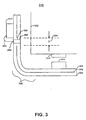
- Figure 3 is a side-view illustration of an exemplary flex circuit assembly 319 comprising exemplary flex circuit 300, an IC 312, and an external electrical sub assembly 322 in accordance with embodiments of the invention.
- the flexible circuit (flex circuit) 300 is multi-layered wherein a ground plane 306 is disposed between transmission line 302 and transmission line 304.
- Ground plane 306 provides increased signal integrity along the signal transmission lines 304 and 302 as well as isolation between transmission lines on opposite sided of flex circuit 300.
- An integrated circuit (IC) 312 is electrically coupled to transmission line 304 by wirebond 435 and a bond pad 456. For clarity one wirebond 435 and one bond pad 456 are illustrated. In accordance with embodiments of the invention, a plurality of wirebonds 435 and bond pads 456 electrically couple IC 312 to transmission line 304, depending on the electrical configuration of IC 312. Also, wirebond bond pads 456 are disposed in a low areal density to accommodate the geometry of the IC 312. Typically, an IC has contact pads on its periphery to allow connection to an external assembly.
- the IC 312 electrically couples to a low areal density bond pad scheme 456 and as a result, vias 455 are disposed proximate the low areal density bond pad scheme 456 without significantly degrading the ground plane 306, thus avoiding degradation of electrical integrity of the flex circuit 300.
- locating vias 455 proximate the low areal density bond pads 456 reduces the distance 564 a signal must travel without the benefits of a ground plane.
- wirebond 435 inherently creates an electrical discontinuity in the flex circuit assembly 319.
- a signal must travel the length of the wire bond from the flex circuit 300 to the IC 312 without the benefit of a ground plane.
- combining discontinuities in a flexible circuit assembly beneficially reduces the degradation of signal integrity in the flex circuit 300. More specifically, in accordance with embodiments of the invention, locating vias at a location of electrical discontinuity reduces the amount of discontinuities in the circuit assembly.
- vias 455 are formed coincident the wirebond bond pads 456.
- Vias 455 can be formed by drilling, laser, etching or using any of the well-known methods in the art for forming vias.
- via plugs 390 are formed in the vias 455 to electrically couple transmission lines 304 and 302 and transfer a signal from the first side of the flex circuit to the other side of the flex circuit while avoiding degradation of signal integrity in flex circuit 300.
- via 455 is plated on the sidewalls with a conductive material to electrically couple transmission lines on opposite sides of flex circuit 300.
- the via can be filled with a conductor by electroplating or any other method known in the art.
- a high areal density electrical interface 314 (e.g., ball grid array (BGA), land grid array (LGA), flip chip pad array, fuzz button) is disposed on the same side of the flex circuit 300 as transmission path 302 (as shown in Figure 3, the high density electrical interface 314 is located on the opposite side of flex circuit 300 as IC 312).
- the electrical interface 314 is disposed with a higher areal density than connector scheme 456 used to electrically couple IC 312 to flex circuit 300.
- any of a number of well-known electrical coupling processes may be used to electrically couple the integrated circuit 312 to the conductors 456 of the flex board 300.
- wirebonding can be employed wherein wires are bonded by thermocompression bonding, ultrasonic or wedge bonding, or by thermosonic bonding, just to name a few.
- wirebonding couples an electrical connector on IC 312 to a bond pad 456 on flex circuit 300. While the foregoing wire bonding processes are well-known in the art and are documented in numerous technical references such as, for example, Electronic Materials Handbook, Volume 1-Packaging, (ASM International, Materials Park, Ohio 44073, 1989), pp. 224-236, which is hereby incorporated by reference, a brief description of each process follows in the interest of providing additional background for the invention.
- Thermocompression bonding is accomplished by bringing the wire and the bonding pad into intimate contact during a controlled time, temperature and pressure cycle.
- a gold wire is threaded through a heated capillary on the wire bonding machine.
- the heated capillary is maintained at a temperature of about 350 degree C.
- a ball is then formed on the end of the wire by either an electronic discharge or a hydrogen flame. Surface tension causes a ball to form on the end of the wire, which is then brought in contact with the heated bonding pad.
- the weld is affected by applying vertical pressure to the ball and wire.
- the capillary is then raised and repositioned over the appropriate conductor on the flex board and the wire bonded thereto by deforming the wire with pressure from the heated capillary.
- a wire clamp within the wire bonding machine is then closed, and the capillary and wire raised, thereby breaking the wire at the heel of the second bond. The process is then repeated for each connection.
- Ultrasonic or wedge-wedge bonding is a low-temperature process in which the source of energy for the metal welding is a transducer vibrating the bonding tool or wedge at an ultrasonic frequency, usually in the range of 20 to 60 kHz.
- the wire is threaded through a hole in the wedge and trailed under the bonding tip.
- the bonding tool is positioned over the first bond site with the wire protruding under and somewhat beyond the front of the wedge.
- the wedge is lowered and the wire is pressed tightly between the wedge and the first bond site.
- a burst of ultrasonic energy is then applied to the wedge which, in combination with the pressure, welds the wire to the pad.
- an electrical sub-assembly 322 can be coupled to flex circuit 300 by electrical connectors 310 and 314.
- the electrical sub-assembly 322 comprises an electrical connector 310 configured to electrically couple to connector 314 on flex circuit 300.
- electrical sub-assembly 322 provides an electrical signal for IC 312.
- electrical sub-assembly can serve as a heat sink for IC 312.
- flex circuit 300 is configured such that IC 312 is contacting sub-assembly 322 wherein sub-assembly 322 is thermally coupled to IC 312 to provide heat sinking.
- Figure 4A is a side-view illustration of an exemplary flex circuit assembly wherein vias 455 are disposed proximate low areal density wirebond bond pads 456 to transfer a signal from transmission line 304 to transmission line 302 while reducing discontinuity in flex circuit 300 in accordance with an embodiment of the invention.
- flex circuit 300 comprises a first transmission line 302, a second transmission line 304, and a ground plane 306 separating transmission line 302 and transmission line 304 to reduce degradation of signal integrity.
- a via 455 passes through ground plane 306 which is drawn back slightly from the via and provides for forming via plug 390 to electrically couple transmission line 302 and transmission line 304.
- a wire bond 435 electrically couples IC 312 to bond pad 456 and via plug 390.
- electrical sub-assembly 322 is thermally coupled to IC 312 and optoelectronic device 430 is coupled to IC 312.
- disposing vias at a location of discontinuity combines discontinuity in flex circuit 300, thus improving signal integrity therein.
- the distance 564 a signal must travel without the benefit of a ground plane proximate thereto is advantageously significantly reduced when vias 455 are disposed proximate low areal density connector pads 456.
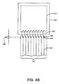
- Figure 4B is a top view illustration of an exemplary flex circuit assembly wherein vias 455 is disposed proximate linearly arranged wirebond bond pad scheme 456 to provide for transferring a signal from a first side of a flex circuit to a second opposing side of the flex circuit while reducing discontinuities in flex circuit 300 in accordance with an embodiment of the invention.
- Figure 4B is a top view illustration of the exemplary circuit assembly illustrated in Figure 4A.
- Figure 4B illustrates a wirebond bond pad scheme 456 where a wire bond 435 electrically couples IC 312 to via plug 390 (shown in Figure 4A).
- Bond pad scheme 456 is arranged linearly, thus the vias 455 disposed proximate the bond pads are disposed linearly, resulting in a linear discontinuity of the ground plane.
- vias 455 are arranged linearly, the distance 564 a signal must travel without the benefits of a ground plane therein is reduced, thus reducing degradation of signal integrity in the flex circuit.
- wirebonds 435 create an element of electrical discontinuity, advantageously, locating vias proximate wirebonds combines discontinuities in the flex circuit 300, thus reducing degradation of signal integrity therein.
- the discontinuity of the flex circuit is combined to a location.
- the fewer discontinuities in the circuit reduction of signal integrity degradation can be achieved.
- the signal crosses fewer discontinuities.
- Figure 5A is a top view illustration of an exemplary flexible circuit assembly comprising exemplary flex circuit 300 with vias 455 disposed proximate a teardrop shaped wirebond bond pad scheme 520 to minimize electrical discontinuity and combine discontinuities in accordance with an embodiment of the invention.
- Figure 5A illustrates a flex circuit 300 having larger dimensions than the IC 312, thus surrounding the IC. This configuration allows bond pads 520 to be disposed proximate the periphery of the IC 312, thus spacing the bond pads 520 and vias 455 with a lower areal density therein.
- the teardrop bond pads 520 can be staggered for closer spacing in flex circuit configurations requiring more transmission lines.
- distance 564 a signal must travel without the benefit of a ground plane does not change when the teardrop bond pads 520 are staggered, because distance 564 is approximately the width of a via 455 and staggering the bonding pads 520 does not alter distance 564.
- the teardrop bond pad 520 is a dual-purpose bond pad because it serves as the capture pad for via 455 and the bond pad for the wirebond 435.
- the footprint of the teardrop shaped bond pad 520 is smaller than if the wirebond and the via had separate pads. By sharing the same pad, higher density of the transmission lines can be achieved because the transmission lines can be spaced closer to each other. For clarity, only a few transmission lines are illustrated.
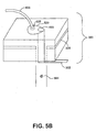
- Figure 5B is a perspective illustration of a portion of a flex circuit with a via 455 disposed proximate the location of a wirebond bond pad 520 to transfer an electrical signal from one side of the flex circuit to the other side of the flex circuit while reducing discontinuity.
- Flex circuit 300 comprises a dual purpose teardrop pad 520 that serves as a bond pad 522 for wirebond 435 and a capture pad for via 455.
- a via plug (not shown for clarity) can be disposed after the via 455 is formed.
- a ground plane 306 is disposed between transmission line 302 and dual purpose pad 522 to increase signal integrity.
- Figure 5C is a top view illustration of a flexible circuit 300 having reduced ground plane discontinuity as a result of vias disposed near a low areal density connector scheme such as wirebond bond pads.
- a low areal density connector scheme such as wirebond bond pads.
- the distance (216 from Prior Art Figure 2B) that a signal must travel without the benefit of a ground plane when disposing vias near a high areal density connector scheme, such as a BGA is relatively large when compared to the smaller distance 564 when the vias are disposed proximate lower areal density wirebond capture pads.
- vias 455 disposed proximate a low areal density connector scheme such as wirebond bond pads 520 reduce discontinuity in flex circuit 300.
- Embodiments of the present invention a via placement for layer transitions in flexible circuits with high density ball grid arrays has been described. While the present invention has been described in particular embodiments, it should be appreciated that the present invention should not be construed as limited by such embodiments, but rather construed according to the following Claims.
Landscapes
- Engineering & Computer Science (AREA)
- Microelectronics & Electronic Packaging (AREA)
- Structure Of Printed Boards (AREA)
Abstract
Description
- The invention relates to flexible circuits and more particularly to a flexible circuit to connect an integrated circuit or other electronics module to a high density ball grid array or any other connector scheme requiring a two dimensional array of closely spaced connection pads.
- A flexible circuit (flex circuit) is a type of electrical connection device that can be bent, twisted or wrapped to fit in extremely small spaces. Flex circuits are excellent for designs with fine line traces and high-density circuitry, and are more suited for dynamic applications and vibration conditions than are conventional printed wiring boards. Using flex circuits sometimes requires transferring an electrical signal from one side of the flex circuit to the opposing side of the flex circuit.
- One solution to transition signals from one side of a flex to another side of a flex is to dispose vias proximate the location of a high areal density connector scheme, such as a ball grid array (BGA). Prior Art Figure 1A illustrates a side view of a
flex circuit 110 comprising afirst surface 240 and a secondopposing surface 245. Flexcircuit 110 has a transmission line 202 onsurface 240 and atransmission line 204 onsurface 245. It is appreciated that a conventional flexible circuit can have a plurality of transmission lines on each surface.Transmission lines 202 and 204 represent one of many transmission lines on each surface of theflex circuit 110. A high arealdensity connector scheme 120 is disposed onsurface 240 and is electrically coupled to transmission line 202.Vias 246 are conventionally disposed proximate the high arealdensity connector scheme 120 to provide for transitioning a signal fromtransmission line 204 to transmission line 202. Aground plane 206 is disposed between transmission line 202 andtransmission line 204 to increase signal integrity in theflex circuit 110. - To manufacture
vias 246 in theflex circuit 110, a hole is formed through theflex circuit 110, including theground plane 206. A deleterious effect of locatingvias 246 proximate the high arealdensity connector scheme 120 is that theground plane 206 becomes significantly discontinuous, thus causing grounding problems in theflex circuit 110. Grounding problems occur because a signal must travel along a transmission line adistance 216 without the benefit of aground plane 206. Prior Art Figure 1B illustrates a top view of a portion of aground plane 206 that is significantly discontinuous as a result ofvias 246 disposedproximate connector scheme 120. In some cases, the density of the connector scheme will result in overlapping ground relief holes, thus essentially removing the entire ground plane from the area under the BGA. In addition, placing vias proximate theBGA 120 introduces an additional element of discontinuity in the transmission path on theflex circuit 110. - In other prior art approaches, the vias are located throughout the flex circuit (i.e., not coincident connector scheme 120) to avoid the grounding problems associated with locating the vias near the high-density connector scheme. However, locating the vias throughout the flex circuit distributes electrical discontinuity throughout the entire flex circuit. Every discontinuity along a transmission line is a possible reflection, thus spreading discontinuities can possibly corrupt transmission of a signal along the entire flex circuit.
- Disclosed is a flexible electrical connector in accordance with the invention that transitions a signal from a transmission line on a first surface to a transmission line on an opposing surface while avoiding degradation of signal integrity. The flexible connector includes a flexible circuit having vias disposed in locations that reduce discontinuity in a ground plane separating transmission lines. By reducing the discontinuity of the ground plane separating the transmission lines, degradation of signal integrity in the flex circuit can be avoided. Furthermore, disposing vias at a location of electrical discontinuity combines discontinuity in the flex circuit, thus further avoiding degradation of signal integrity.
- The accompanying drawings, which are incorporated in and form a part of this specification, illustrate embodiments of the invention and, together with the description, serve to explain the principles of the invention.
- Figure 1 A is a prior art side view illustration of a conventional two-layer flex circuit comprising vias located near a high areal density connector scheme for transitioning a signal from one side to the other side.
- Figure 1 B is a prior art top view illustration of the ground plane in the conventional two-layer flex circuit of prior art Figure 1A illustrating the discontinuity of the ground plane surrounding vias located near a high areal density connector scheme.
- Figure 2 is a side view illustration of an exemplary flexible circuit comprising vias located proximate a low areal density connector scheme in accordance with an embodiment of the invention.
- Figure 3 is a side view illustration of an exemplary flexible circuit assembly comprising vias proximate a low areal density connector scheme connecting an IC to the exemplary flex circuit in accordance with an embodiment of the invention.
- Figure 4A is a side view illustration of the exemplary flexible circuit in Figure 3 further comprising a heat sink in accordance with an embodiment of the invention.
- Figure 4B is a top view illustration of an exemplary flexible circuit comprising vias proximate a low-density connector scheme to provide for transferring a signal from a first side of the circuit to a second opposing side of the flex circuit in accordance with an embodiment of the invention.
- Figure 5A is a top view illustration of an exemplary flexible circuit comprising vias disposed linearly proximate a low areal density connector scheme to minimize discontinuity in a transmission path in accordance to an embodiment of the invention.
- Figure 5B is a perspective illustration of an exemplary flexible circuit having a via disposed proximate a teardrop shaped wirebond capture pad to minimize discontinuity in a ground plane in accordance with an embodiment of the invention.
- Figure 5C is a top view illustration of an exemplary flex circuit having a minimized discontinuity in a ground plane in accordance with an embodiment of the invention.
- Reference will now be made in detail to the various embodiments of the invention, examples of which are illustrated in the accompanying drawings. While the invention will be described in conjunction with the various embodiments, it will be understood that they are not intended to limit the invention to these embodiments. On the contrary, the invention is intended to cover alternatives, modifications and equivalents, which may be included within the invention as defined by the appended claims.
- Furthermore, in the following detailed description of the present invention, numerous specific details are set forth in order to provide a thorough understanding of the present invention. However, it will be obvious to one of ordinary skill in the art that the present invention may be practiced without these specific details.. In other instances, well-known methods, procedures, components, and circuits have not been described in detail as not to unnecessarily obscure aspects of the present invention.
- Figure 2 is a side-view illustration of an exemplary
flexible circuit 300 havingvias 455 disposed to reduce discontinuity in aground plane 306 separating opposing transmission lines in accordance with embodiments of the invention. Flexcircuit 300 has afirst transmission line 302 disposed on one surface of theflexible circuit 300 and asecond transmission line 304 disposed on an opposing surface of theflexible circuit 300. It is appreciated thattransmission lines flex circuit 300. For clarity, a single transmission line is illustrated on each surface. In accordance with embodiments of the invention,flex circuit 300 has a plurality of transmission lines on each surface wherein a via electrically couples a single transmission line on one side to a single transmission line on an opposite side offlex circuit 300. A top view offlex circuit 300 is illustrated in Figure 4B wherein a plurality of transmission lines are on a side offlex circuit 300. Aground plane 306 is disposed betweentransmission line 302 andtransmission line 304 to improve signal integrity along the transmission lines and to isolate the transmission lines on opposite sides of the flex circuit. Theflexible circuit 300 also comprises low areal densityelectrical connection pads 456 electrically coupled totransmission line 304. The flexible circuit also includes higher areal densityelectrical connection pads 314 electrically coupled totransmission line 302. In embodiments in accordance with the invention,vias 455 are disposed coincident the lower areal densityelectrical connection pads 456. In so doing, embodiments in accordance with the invention provide for electricallycoupling transmission line 302 andtransmission line 304 while reducing electrical discontinuity inflex circuit 300. Also, the lower areal density ofconnection pads 456 enable disposing vias for transitioning of a signal fromtransmission line 304 totransmission line 302 without causing significant discontinuity ofground plane 306. In addition, locatingvias 455 close to an existing discontinuity on flex circuit combines the discontinuities, thus further improving signal transmission inflex circuit 300. - As stated above, every discontinuity along a transmission line is a possible reflection, thus possibly corrupting transmission of a signal along the line. In accordance with embodiments of the
invention vias 455 are located proximate the lower arealdensity connection pads 456 to reduce the amount of discontinuity inground plane 306, thus improving signal transmission in theflex circuit 300. By reducing the discontinuity of the ground plane, the distance 564 a signal must travel without the benefits of a ground plane is reduced, thus increasing signal integrity in theflex circuit 300. Furthermore,distance 564 is approximately the width of avia 455, wherein the prior art, the distance (216 from Prior Art Figures 1A and 1B) is multiple times the width of a via. - Figure 3 is a side-view illustration of an exemplary
flex circuit assembly 319 comprisingexemplary flex circuit 300, anIC 312, and an externalelectrical sub assembly 322 in accordance with embodiments of the invention. In accordance with an embodiment of the invention, the flexible circuit (flex circuit) 300 is multi-layered wherein aground plane 306 is disposed betweentransmission line 302 andtransmission line 304.Ground plane 306 provides increased signal integrity along thesignal transmission lines flex circuit 300. - An integrated circuit (IC) 312 is electrically coupled to
transmission line 304 bywirebond 435 and abond pad 456. For clarity onewirebond 435 and onebond pad 456 are illustrated. In accordance with embodiments of the invention, a plurality ofwirebonds 435 andbond pads 456electrically couple IC 312 totransmission line 304, depending on the electrical configuration ofIC 312. Also,wirebond bond pads 456 are disposed in a low areal density to accommodate the geometry of theIC 312. Typically, an IC has contact pads on its periphery to allow connection to an external assembly. Furthermore, theIC 312 electrically couples to a low areal densitybond pad scheme 456 and as a result, vias 455 are disposed proximate the low areal densitybond pad scheme 456 without significantly degrading theground plane 306, thus avoiding degradation of electrical integrity of theflex circuit 300. In addition, locatingvias 455 proximate the low arealdensity bond pads 456 reduces the distance 564 a signal must travel without the benefits of a ground plane. - Moreover, wirebond 435 inherently creates an electrical discontinuity in the
flex circuit assembly 319. A signal must travel the length of the wire bond from theflex circuit 300 to theIC 312 without the benefit of a ground plane. According to embodiments of the invention, combining discontinuities in a flexible circuit assembly (locating vias 455 at a location of a discontinuity) beneficially reduces the degradation of signal integrity in theflex circuit 300. More specifically, in accordance with embodiments of the invention, locating vias at a location of electrical discontinuity reduces the amount of discontinuities in the circuit assembly. - In accordance with embodiments of the invention, vias 455 are formed coincident the
wirebond bond pads 456.Vias 455 can be formed by drilling, laser, etching or using any of the well-known methods in the art for forming vias. After vias 455 are formed, viaplugs 390 are formed in thevias 455 to electricallycouple transmission lines flex circuit 300. In accordance with an embodiment of the invention, via 455 is plated on the sidewalls with a conductive material to electrically couple transmission lines on opposite sides offlex circuit 300. The via can be filled with a conductor by electroplating or any other method known in the art. - A high areal density electrical interface 314 (e.g., ball grid array (BGA), land grid array (LGA), flip chip pad array, fuzz button) is disposed on the same side of the
flex circuit 300 as transmission path 302 (as shown in Figure 3, the high densityelectrical interface 314 is located on the opposite side offlex circuit 300 as IC 312). In accordance with embodiments of the present invention, theelectrical interface 314 is disposed with a higher areal density thanconnector scheme 456 used to electrically coupleIC 312 to flexcircuit 300. - Any of a number of well-known electrical coupling processes may be used to electrically couple the
integrated circuit 312 to theconductors 456 of theflex board 300. For example, wirebonding can be employed wherein wires are bonded by thermocompression bonding, ultrasonic or wedge bonding, or by thermosonic bonding, just to name a few. In accordance with embodiments of the invention, wirebonding couples an electrical connector onIC 312 to abond pad 456 onflex circuit 300. While the foregoing wire bonding processes are well-known in the art and are documented in numerous technical references such as, for example, Electronic Materials Handbook, Volume 1-Packaging, (ASM International, Materials Park, Ohio 44073, 1989), pp. 224-236, which is hereby incorporated by reference, a brief description of each process follows in the interest of providing additional background for the invention. - Thermocompression bonding is accomplished by bringing the wire and the bonding pad into intimate contact during a controlled time, temperature and pressure cycle. In one example of a thermocompression wire bonding process, a gold wire is threaded through a heated capillary on the wire bonding machine. The heated capillary is maintained at a temperature of about 350 degree C. A ball is then formed on the end of the wire by either an electronic discharge or a hydrogen flame. Surface tension causes a ball to form on the end of the wire, which is then brought in contact with the heated bonding pad. The weld is affected by applying vertical pressure to the ball and wire. The capillary is then raised and repositioned over the appropriate conductor on the flex board and the wire bonded thereto by deforming the wire with pressure from the heated capillary. A wire clamp within the wire bonding machine is then closed, and the capillary and wire raised, thereby breaking the wire at the heel of the second bond. The process is then repeated for each connection.
- Ultrasonic or wedge-wedge bonding is a low-temperature process in which the source of energy for the metal welding is a transducer vibrating the bonding tool or wedge at an ultrasonic frequency, usually in the range of 20 to 60 kHz. In the ultrasonic process, the wire is threaded through a hole in the wedge and trailed under the bonding tip. The bonding tool is positioned over the first bond site with the wire protruding under and somewhat beyond the front of the wedge. The wedge is lowered and the wire is pressed tightly between the wedge and the first bond site. A burst of ultrasonic energy is then applied to the wedge which, in combination with the pressure, welds the wire to the pad. The wedge is moved over to the second bond site, lowered and ultrasonic energy is again applied to the wedge, thus bonding the wire to the second bond site. The wedge is then rocked slightly to weaken the wire at the heel of the second bond and a clamp inside the wedge is then closed and the wedge raised, separating the wire from the bond.
- Referring to Figure 3 again, an
electrical sub-assembly 322 can be coupled to flexcircuit 300 byelectrical connectors electrical sub-assembly 322 comprises anelectrical connector 310 configured to electrically couple toconnector 314 onflex circuit 300. Furthermore,electrical sub-assembly 322 provides an electrical signal forIC 312. In addition to providing a signal toIC 312, electrical sub-assembly can serve as a heat sink forIC 312. Additionally,flex circuit 300 is configured such thatIC 312 is contactingsub-assembly 322 whereinsub-assembly 322 is thermally coupled toIC 312 to provide heat sinking. - Figure 4A is a side-view illustration of an exemplary flex circuit assembly wherein
vias 455 are disposed proximate low areal densitywirebond bond pads 456 to transfer a signal fromtransmission line 304 totransmission line 302 while reducing discontinuity inflex circuit 300 in accordance with an embodiment of the invention. As stated,flex circuit 300 comprises afirst transmission line 302, asecond transmission line 304, and aground plane 306 separatingtransmission line 302 andtransmission line 304 to reduce degradation of signal integrity. A via 455 passes throughground plane 306 which is drawn back slightly from the via and provides for forming viaplug 390 to electricallycouple transmission line 302 andtransmission line 304. Awire bond 435electrically couples IC 312 tobond pad 456 and viaplug 390. In accordance with embodiments of the invention,electrical sub-assembly 322 is thermally coupled toIC 312 andoptoelectronic device 430 is coupled toIC 312. As stated above, disposing vias at a location of discontinuity combines discontinuity inflex circuit 300, thus improving signal integrity therein. In addition, the distance 564 a signal must travel without the benefit of a ground plane proximate thereto is advantageously significantly reduced whenvias 455 are disposed proximate low arealdensity connector pads 456. - Figure 4B is a top view illustration of an exemplary flex circuit assembly wherein
vias 455 is disposed proximate linearly arranged wirebondbond pad scheme 456 to provide for transferring a signal from a first side of a flex circuit to a second opposing side of the flex circuit while reducing discontinuities inflex circuit 300 in accordance with an embodiment of the invention. Figure 4B is a top view illustration of the exemplary circuit assembly illustrated in Figure 4A. Figure 4B illustrates a wirebondbond pad scheme 456 where awire bond 435electrically couples IC 312 to via plug 390 (shown in Figure 4A).Bond pad scheme 456 is arranged linearly, thus thevias 455 disposed proximate the bond pads are disposed linearly, resulting in a linear discontinuity of the ground plane. Beneficially, when vias 455 are arranged linearly, the distance 564 a signal must travel without the benefits of a ground plane therein is reduced, thus reducing degradation of signal integrity in the flex circuit. Additionally, since wirebonds 435 create an element of electrical discontinuity, advantageously, locating vias proximate wirebonds combines discontinuities in theflex circuit 300, thus reducing degradation of signal integrity therein. By locating a via at a location of discontinuity, the discontinuity of the flex circuit is combined to a location. Beneficially, the fewer discontinuities in the circuit, reduction of signal integrity degradation can be achieved. By combining the discontinuities in the flex circuit, the signal crosses fewer discontinuities. - In addition, by locating
vias 455 proximate the location of thewire bond 435, the wirebond bond pad and the via capture pad can be combined into onepad 456. In accordance with embodiments of the invention, a teardrop shaped bond pad is used to combine the wirebond bond pad and the via capture pad. The method of manufacturing teardrop shaped bond pads is well known in the art. - Figure 5A is a top view illustration of an exemplary flexible circuit assembly comprising
exemplary flex circuit 300 withvias 455 disposed proximate a teardrop shaped wirebondbond pad scheme 520 to minimize electrical discontinuity and combine discontinuities in accordance with an embodiment of the invention. Figure 5A illustrates aflex circuit 300 having larger dimensions than theIC 312, thus surrounding the IC. This configuration allowsbond pads 520 to be disposed proximate the periphery of theIC 312, thus spacing thebond pads 520 and vias 455 with a lower areal density therein. In accordance with embodiments of the invention, theteardrop bond pads 520 can be staggered for closer spacing in flex circuit configurations requiring more transmission lines. In addition, the distance 564 a signal must travel without the benefit of a ground plane does not change when theteardrop bond pads 520 are staggered, becausedistance 564 is approximately the width of a via 455 and staggering thebonding pads 520 does not alterdistance 564. - The
teardrop bond pad 520 is a dual-purpose bond pad because it serves as the capture pad for via 455 and the bond pad for thewirebond 435. The footprint of the teardrop shapedbond pad 520 is smaller than if the wirebond and the via had separate pads. By sharing the same pad, higher density of the transmission lines can be achieved because the transmission lines can be spaced closer to each other. For clarity, only a few transmission lines are illustrated. - Figure 5B is a perspective illustration of a portion of a flex circuit with a via 455 disposed proximate the location of a
wirebond bond pad 520 to transfer an electrical signal from one side of the flex circuit to the other side of the flex circuit while reducing discontinuity.Flex circuit 300 comprises a dualpurpose teardrop pad 520 that serves as abond pad 522 forwirebond 435 and a capture pad for via 455. As stated, a via plug (not shown for clarity) can be disposed after the via 455 is formed. Aground plane 306 is disposed betweentransmission line 302 anddual purpose pad 522 to increase signal integrity. As stated above, when via 455 is formed, a portion of theground plane 306 is removed and as a result, a signal must traverse adistance 564 without the benefit of aground plane 306 therein. Thedistance 564 that the signal must travel without the benefits of a ground plane is reduced when the via is disposed proximate thewirebond bond pad 520. More specifically, the amount of discontinuity in the ground plane is less when vias are disposed at a lower areal density connector scheme. - Figure 5C is a top view illustration of a
flexible circuit 300 having reduced ground plane discontinuity as a result of vias disposed near a low areal density connector scheme such as wirebond bond pads. As described above, the distance (216 from Prior Art Figure 2B) that a signal must travel without the benefit of a ground plane when disposing vias near a high areal density connector scheme, such as a BGA, is relatively large when compared to thesmaller distance 564 when the vias are disposed proximate lower areal density wirebond capture pads. In accordance with an embodiment of the invention, vias 455 disposed proximate a low areal density connector scheme such aswirebond bond pads 520 reduce discontinuity inflex circuit 300. It is appreciated thatwirebond pad 520 may also be a dual-purpose wirebond bond pad and a via capture pad (e.g., teardrop shapedpad 520 from Figure 5B). Asignal line 302 can be routed such that it must only travel adistance 564 without the benefit of a ground plane, thus improving signal integrity inflex circuit 300.Transmission line 304 resides betweenbond pads 520 andvias 455. When compared to the amount of discontinuity inherent in a wirebond, the additional element of discontinuity incurred by the via is negligible, therefore, combining discontinuities further improves signal integrity inflex circuit 300. - Embodiments of the present invention, a via placement for layer transitions in flexible circuits with high density ball grid arrays has been described. While the present invention has been described in particular embodiments, it should be appreciated that the present invention should not be construed as limited by such embodiments, but rather construed according to the following Claims.
- The foregoing descriptions of specific embodiments of the present invention have been presented for purposes of illustration and description. They are not intended to be exhaustive or to limit the invention to the precise forms disclosed, and obviously many modifications and variations are possible in light of the above teaching. The embodiments were chosen and described in order to best explain the principles of the invention and its practical application, to thereby enable others skilled in the art to best utilize the invention and various embodiments with various modifications as are suited to the particular use contemplated. It is intended that the scope of the invention be defined by the Claims appended hereto and their equivalents.
Claims (10)
- A flexible circuit (300) having vias (455) disposed to minimize discontinuity in a ground plane (306) separating opposing transmission lines, said flex circuit (300) comprising:a first type of electrical connection pads (456) disposed on a first surface of said flexible circuit (300), and electrically coupled to a first transmission line (304);a second type of electrical connection pads (314) disposed on a second surface of said flexible circuit (300), and electrically coupled to a second transmission line (302) wherein said second type of electrical connection pads (314) have a higher areal density than said first type of electrical connection pads (456); andvias (455) disposed proximate said first type of electrical connection pads (456) and extending through a ground plane (306) to provide for electrically coupling said first transmission line (304) and said second transmission line (302), such that said vias (455) minimize discontinuity in said ground plane (306).
- The flexible circuit (300) as described in Claim 1 wherein said first type of electrical connection pads (456) are flip-chip pads.
- The flexible circuit (300) as described in Claim 1 wherein said first type of electrical connection pads (456) are wirebond bond pads.
- The flexible circuit (300) as described in Claim 3 wherein at least one of said plurality of vias (455) is coincident with one of said plurality of wirebond bond pads (456).
- The flexible circuit (300) as described in Claim 2 wherein at least one of said plurality of vias (455) is coincident with one of said plurality of flip-chip pads.
- The flexible circuit (300) as described in Claim 4 wherein at least one of said plurality of wirebond bond pads is substantially tear-dropped shaped (520).
- The flexible circuit (300) as described in Claim 5 wherein at least one of said plurality of flip-chip pads is substantially tear-dropped shaped (520).
- The flexible circuit (300) as described in any of Claims 1 to 7 wherein said first type of electrical connection pads (456) are configured for coupling an integrated circuit (312) thereto.
- The flexible circuit (300) as described in any of Claims 1 to 8 wherein said first type of electrical connection pads (456) are configured for coupling an optical module (430) thereto.
- The flexible circuit (300) as described in any of Claims 1 to 9 wherein said second type of electrical connection pads (314) are a ball grid array or pin grid array.
Applications Claiming Priority (2)
| Application Number | Priority Date | Filing Date | Title |
|---|---|---|---|
| US669982 | 2003-09-23 | ||
| US10/669,982 US7223924B2 (en) | 2003-09-23 | 2003-09-23 | Via placement for layer transitions in flexible circuits with high density ball grid arrays |
Publications (1)
| Publication Number | Publication Date |
|---|---|
| EP1519413A1 true EP1519413A1 (en) | 2005-03-30 |
Family
ID=34194814
Family Applications (1)
| Application Number | Title | Priority Date | Filing Date |
|---|---|---|---|
| EP04010830A Withdrawn EP1519413A1 (en) | 2003-09-23 | 2004-05-06 | Via placement for layer transitions in flexible circuits with high density ball grid arrays |
Country Status (4)
| Country | Link |
|---|---|
| US (1) | US7223924B2 (en) |
| EP (1) | EP1519413A1 (en) |
| JP (1) | JP4594016B2 (en) |
| SG (1) | SG110122A1 (en) |
Cited By (2)
| Publication number | Priority date | Publication date | Assignee | Title |
|---|---|---|---|---|
| WO2017080816A1 (en) * | 2015-11-09 | 2017-05-18 | Robert Bosch Gmbh | Contacting arrangement for a circuit board substrate, and method for contacting a circuit board substrate |
| CN109655733A (en) * | 2018-11-26 | 2019-04-19 | 西南电子技术研究所(中国电子科技集团公司第十研究所) | The method of non-destructive testing millimeter wave bga component |
Families Citing this family (6)
| Publication number | Priority date | Publication date | Assignee | Title |
|---|---|---|---|---|
| US10026720B2 (en) | 2015-05-20 | 2018-07-17 | Broadpak Corporation | Semiconductor structure and a method of making thereof |
| US8014166B2 (en) * | 2008-09-06 | 2011-09-06 | Broadpak Corporation | Stacking integrated circuits containing serializer and deserializer blocks using through silicon via |
| US9893004B2 (en) | 2011-07-27 | 2018-02-13 | Broadpak Corporation | Semiconductor interposer integration |
| US9818680B2 (en) | 2011-07-27 | 2017-11-14 | Broadpak Corporation | Scalable semiconductor interposer integration |
| US8810020B2 (en) * | 2012-06-22 | 2014-08-19 | Freescale Semiconductor, Inc. | Semiconductor device with redistributed contacts |
| KR101442354B1 (en) | 2012-12-21 | 2014-09-17 | 삼성전기주식회사 | Pre space transformer and space transformer manufactured by the pre space transformer, and apparatus for inspecting semiconductor device with the space transformer |
Citations (5)
| Publication number | Priority date | Publication date | Assignee | Title |
|---|---|---|---|---|
| US5362656A (en) * | 1992-12-02 | 1994-11-08 | Intel Corporation | Method of making an electronic assembly having a flexible circuit wrapped around a substrate |
| US5448020A (en) * | 1993-12-17 | 1995-09-05 | Pendse; Rajendra D. | System and method for forming a controlled impedance flex circuit |
| US5635424A (en) * | 1992-07-17 | 1997-06-03 | Lsi Logic Corporation | High-density bond pad layout arrangements for semiconductor dies, and connecting to the bond pads |
| JP2001352000A (en) * | 2000-06-05 | 2001-12-21 | New Japan Radio Co Ltd | High frequency semiconductor device using interposer |
| US20030164541A1 (en) * | 2002-03-04 | 2003-09-04 | Lee Teck Kheng | Method and apparatus for dielectric filling of flip chip on interposer assembly |
Family Cites Families (8)
| Publication number | Priority date | Publication date | Assignee | Title |
|---|---|---|---|---|
| US6962829B2 (en) * | 1996-10-31 | 2005-11-08 | Amkor Technology, Inc. | Method of making near chip size integrated circuit package |
| JP3961092B2 (en) * | 1997-06-03 | 2007-08-15 | 株式会社東芝 | Composite wiring board, flexible substrate, semiconductor device, and method of manufacturing composite wiring board |
| US6064113A (en) * | 1998-01-13 | 2000-05-16 | Lsi Logic Corporation | Semiconductor device package including a substrate having bonding fingers within an electrically conductive ring surrounding a die area and a combined power and ground plane to stabilize signal path impedances |
| US6396712B1 (en) * | 1998-02-12 | 2002-05-28 | Rose Research, L.L.C. | Method and apparatus for coupling circuit components |
| JP2000228461A (en) * | 1998-09-29 | 2000-08-15 | Kyocera Corp | High frequency wiring board |
| JP2000353767A (en) * | 1999-05-14 | 2000-12-19 | Universal Instr Corp | Substrate for mounting electronic components, package, mounting method, and method of housing integrated circuit chip in package |
| US6586682B2 (en) * | 2000-02-23 | 2003-07-01 | Kulicke & Soffa Holdings, Inc. | Printed wiring board with controlled line impedance |
| US6762367B2 (en) * | 2002-09-17 | 2004-07-13 | International Business Machines Corporation | Electronic package having high density signal wires with low resistance |
-
2003
- 2003-09-23 US US10/669,982 patent/US7223924B2/en not_active Expired - Lifetime
-
2004
- 2004-05-06 EP EP04010830A patent/EP1519413A1/en not_active Withdrawn
- 2004-09-06 SG SG200404945A patent/SG110122A1/en unknown
- 2004-09-22 JP JP2004274729A patent/JP4594016B2/en not_active Expired - Fee Related
Patent Citations (5)
| Publication number | Priority date | Publication date | Assignee | Title |
|---|---|---|---|---|
| US5635424A (en) * | 1992-07-17 | 1997-06-03 | Lsi Logic Corporation | High-density bond pad layout arrangements for semiconductor dies, and connecting to the bond pads |
| US5362656A (en) * | 1992-12-02 | 1994-11-08 | Intel Corporation | Method of making an electronic assembly having a flexible circuit wrapped around a substrate |
| US5448020A (en) * | 1993-12-17 | 1995-09-05 | Pendse; Rajendra D. | System and method for forming a controlled impedance flex circuit |
| JP2001352000A (en) * | 2000-06-05 | 2001-12-21 | New Japan Radio Co Ltd | High frequency semiconductor device using interposer |
| US20030164541A1 (en) * | 2002-03-04 | 2003-09-04 | Lee Teck Kheng | Method and apparatus for dielectric filling of flip chip on interposer assembly |
Non-Patent Citations (1)
| Title |
|---|
| PATENT ABSTRACTS OF JAPAN vol. 2002, no. 04 4 August 2002 (2002-08-04) * |
Cited By (3)
| Publication number | Priority date | Publication date | Assignee | Title |
|---|---|---|---|---|
| WO2017080816A1 (en) * | 2015-11-09 | 2017-05-18 | Robert Bosch Gmbh | Contacting arrangement for a circuit board substrate, and method for contacting a circuit board substrate |
| CN109655733A (en) * | 2018-11-26 | 2019-04-19 | 西南电子技术研究所(中国电子科技集团公司第十研究所) | The method of non-destructive testing millimeter wave bga component |
| CN109655733B (en) * | 2018-11-26 | 2020-11-24 | 西南电子技术研究所(中国电子科技集团公司第十研究所) | Method for nondestructive testing of millimeter wave BGA packaging assembly |
Also Published As
| Publication number | Publication date |
|---|---|
| US7223924B2 (en) | 2007-05-29 |
| US20050061545A1 (en) | 2005-03-24 |
| SG110122A1 (en) | 2005-04-28 |
| JP2005101612A (en) | 2005-04-14 |
| JP4594016B2 (en) | 2010-12-08 |
Similar Documents
| Publication | Publication Date | Title |
|---|---|---|
| US8008785B2 (en) | Microelectronic assembly with joined bond elements having lowered inductance | |
| US6534879B2 (en) | Semiconductor chip and semiconductor device having the chip | |
| US8637975B1 (en) | Semiconductor device having lead wires connecting bonding pads formed on opposite sides of a core region forming a shield area | |
| US5468994A (en) | High pin count package for semiconductor device | |
| KR19990029932A (en) | Method and apparatus for wire bond package for integrated circuits | |
| US8022558B2 (en) | Semiconductor package with ribbon with metal layers | |
| US8778732B2 (en) | Microelectronic devices and microelectronic support devices, and associated assemblies and methods | |
| US6911734B2 (en) | Semiconductor device and electronic device | |
| US6891260B1 (en) | Integrated circuit package substrate with high density routing mechanism | |
| CN100573858C (en) | chip package | |
| US7330084B2 (en) | Printed circuit board having a bond wire shield structure for a signal transmission line | |
| US7223924B2 (en) | Via placement for layer transitions in flexible circuits with high density ball grid arrays | |
| TW512503B (en) | Integrated circuit package having partially exposed conductive layer | |
| US20110147928A1 (en) | Microelectronic assembly with bond elements having lowered inductance | |
| CN1332440C (en) | Semiconductor device | |
| US6777802B1 (en) | Integrated circuit package substrate with multiple voltage supplies | |
| JP3998562B2 (en) | Semiconductor device | |
| KR101003393B1 (en) | Microelectronic Assemblies with Junction Configurations Reduce Inductance | |
| JP2012248877A (en) | Semiconductor package having low speed and high speed signal paths | |
| US7279778B2 (en) | Semiconductor package having a high-speed signal input/output terminal | |
| CN101894813B (en) | Semiconductor package structure and manufacturing method thereof | |
| JP2007235149A (en) | Semiconductor device and electronic device | |
| JP2796394B2 (en) | Repair connection method for input / output pins | |
| JP2010161416A (en) | Electronic device | |
| KR20080052053A (en) | Semiconductor Package With Ground Conductor |
Legal Events
| Date | Code | Title | Description |
|---|---|---|---|
| PUAI | Public reference made under article 153(3) epc to a published international application that has entered the european phase |
Free format text: ORIGINAL CODE: 0009012 |
|
| AK | Designated contracting states |
Kind code of ref document: A1 Designated state(s): AT BE BG CH CY CZ DE DK EE ES FI FR GB GR HU IE IT LI LU MC NL PL PT RO SE SI SK TR |
|
| AX | Request for extension of the european patent |
Extension state: AL HR LT LV MK |
|
| 17P | Request for examination filed |
Effective date: 20050817 |
|
| AKX | Designation fees paid |
Designated state(s): DE FR GB IT |
|
| RAP1 | Party data changed (applicant data changed or rights of an application transferred) |
Owner name: AVAGO TECHNOLOGIES GENERAL IP (SINGAPORE) PTE. LTD |
|
| 17Q | First examination report despatched |
Effective date: 20071119 |
|
| STAA | Information on the status of an ep patent application or granted ep patent |
Free format text: STATUS: THE APPLICATION IS DEEMED TO BE WITHDRAWN |
|
| 18D | Application deemed to be withdrawn |
Effective date: 20101201 |