EP1519306B1 - Memory tag and reader - Google Patents
Memory tag and reader Download PDFInfo
- Publication number
- EP1519306B1 EP1519306B1 EP04104692A EP04104692A EP1519306B1 EP 1519306 B1 EP1519306 B1 EP 1519306B1 EP 04104692 A EP04104692 A EP 04104692A EP 04104692 A EP04104692 A EP 04104692A EP 1519306 B1 EP1519306 B1 EP 1519306B1
- Authority
- EP
- European Patent Office
- Prior art keywords
- reader
- data unit
- memory
- sequence number
- memory tag
- Prior art date
- Legal status (The legal status is an assumption and is not a legal conclusion. Google has not performed a legal analysis and makes no representation as to the accuracy of the status listed.)
- Expired - Fee Related
Links
Images


Classifications
-
- G—PHYSICS
- G06—COMPUTING; CALCULATING OR COUNTING
- G06K—GRAPHICAL DATA READING; PRESENTATION OF DATA; RECORD CARRIERS; HANDLING RECORD CARRIERS
- G06K19/00—Record carriers for use with machines and with at least a part designed to carry digital markings
- G06K19/06—Record carriers for use with machines and with at least a part designed to carry digital markings characterised by the kind of the digital marking, e.g. shape, nature, code
- G06K19/067—Record carriers with conductive marks, printed circuits or semiconductor circuit elements, e.g. credit or identity cards also with resonating or responding marks without active components
- G06K19/07—Record carriers with conductive marks, printed circuits or semiconductor circuit elements, e.g. credit or identity cards also with resonating or responding marks without active components with integrated circuit chips
- G06K19/0723—Record carriers with conductive marks, printed circuits or semiconductor circuit elements, e.g. credit or identity cards also with resonating or responding marks without active components with integrated circuit chips the record carrier comprising an arrangement for non-contact communication, e.g. wireless communication circuits on transponder cards, non-contact smart cards or RFIDs
-
- G—PHYSICS
- G06—COMPUTING; CALCULATING OR COUNTING
- G06K—GRAPHICAL DATA READING; PRESENTATION OF DATA; RECORD CARRIERS; HANDLING RECORD CARRIERS
- G06K7/00—Methods or arrangements for sensing record carriers, e.g. for reading patterns
- G06K7/0008—General problems related to the reading of electronic memory record carriers, independent of its reading method, e.g. power transfer
Landscapes
- Engineering & Computer Science (AREA)
- Physics & Mathematics (AREA)
- General Physics & Mathematics (AREA)
- Theoretical Computer Science (AREA)
- Computer Networks & Wireless Communication (AREA)
- Computer Hardware Design (AREA)
- Microelectronics & Electronic Packaging (AREA)
- Artificial Intelligence (AREA)
- Computer Vision & Pattern Recognition (AREA)
- Near-Field Transmission Systems (AREA)
- Burglar Alarm Systems (AREA)
Description
- This invention relates to a memory tag powered by a signal generated by a reader, and a reader.
- Memory tags in the form of Radio Frequency Identification (RFID) tags are well known in the prior art, and the technology is well established (see for example: RFID Handbook, Klaus Finkenzeller, 1999, John Wiley & Sons). RFID tags come in many forms but all comprise an integrated circuit with information stored on it and a coil which enables it to be interrogated by a read/write device generally referred to as a reader. Until recently RFID tags have been quite large, due to the frequency they operate at (13.56MHz) and the size of coil they thus require, and have had very small storage capacities. Such RFID tags have tended to be used in quite simple applications, such as for file tracking within offices or in place of or in addition to bar codes for product identification and supply chain management.
- Much smaller RFID tags have also been developed, operating at various frequencies. For example Hitachi-Maxell have developed "coil-on-chip" technology in which the coil required for the inductive link is on the chip rather than attached to it. This results in a memory tag in the form of a chip of 2.5mm square, which operates at 13.56MHz. In addition Hitachi has developed a memory tag referred to as a "mu-chip" which is a chip of 0.4mm square and operates at 2.45GHz. These smaller memory tags can be used in a variety of different applications. Some are even available for the tagging of pets by implantation.
- Although it is known to provide tags with their own power source, in many applications the tag is also powered by the radio frequency signal generated by the reader. Such a known system is shown in
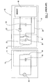
Figure 1 where a reader is indicated generally at 10 and a tag at 12. Thereader 10 comprises aradio frequency generator 13 and aresonant circuit part 11, in the present example comprising aninductor 14 and acapacitor 15 connected in parallel. Theinductor 14 comprises an antenna. The resonant circuit part will have a particular resonant frequency in accordance with the capacitance and inductance of thecapacitor 15 and theinductor 14, and thefrequency generator 13 is operated to generate a signal at that resonant frequency. - The
tag 12 similarly comprises a resonant circuit part generally illustrated at 16, a rectifying circuit part generally indicated at 17 and amemory 18. Theresonant circuit part 16 comprises aninductor 19 which again comprises in this example a loop antenna, and acapacitor 20. Theresonant circuit part 16 will thus have a resonant frequency set by theinductor 19 andcapacitor 20. The resonant frequency of theresonant circuit part 16 is selected to be the same as that of thereader 10. The rectifying part comprises a forward-biased diode 21 and acapacitor 22 and thus effectively acts as a half-wave rectifier. - When the
reader 10 and thetag 12 are sufficiently close, a signal generated by thefrequency generator 13 will cause theresonant circuit part 11 to generate a reader signal comprising a high frequency electromagnetic field. When theresonant circuit part 16 is located within this field, a current will be caused to flow in theresonant circuit part 16, drawing power from the time varying magnetic field generated by the reader. The rectifyingcircuit part 17 will then serve to smooth the voltage across the resonant frequency part and provide a power supply storage. The rectifyingcircuit part 17 is sufficient to supply a sufficiently stable voltage to thememory 18 for the memory to operate. - To transmit data from the tag to the reader, the resonant circuit part is also provided with a
switch 23, here comprising a field effect transistor (FET). The FET is connected to the memory by acontrol line 24. When theswitch 23 is closed, it causes an increased current to flow in the tagresonant circuit part 16. This increase in current flow in the tag results in an increased current flow in the reader'sresonant circuit part 11 which can be detected as a change in voltage drop across thereader inductor 14. Thus, by controlling theswitch 23, data stored in thememory 18 of thetag 12 can be transmitted to thereader 10. - With such known tags when power is supplied to the tag, the tag transmits its stored data in a continuous loop, referred to as a "data carousel". If the data received by the reader is corrupted or erroneous in any way, the reader simply waits for the data to be retransmitted. Where the tag only holds a relatively small amount of data, such as the 128 bits held by the Hitachi-Maxell mu-chip, this does not cause any particular disadvantage. Where, however, a tag is provided with a larger memory, simply waiting for the data to be retransmitted may be excessively time consuming.
- In so-called simplex transmission systems, where there is no way of communicating to the transmitting station that a packet is not being correctly received, it is known to use forward error control codes which permit even substantially corrupted data to be recovered without requiring retransmission of the data, but this adds significantly to the quantity of data to be transmitted.
- Where data is transmitted as packets, it also known to provide validation information as part of the packet, a check sum or a cyclic redundancy check code so that the receiving system can check the validity of the data received, but this requires some way of asking the transmitting system to retransmit corrupted packets or, where this is not possible, again waiting for the packet to be retransmitted as part of the data carousel.
- United States patent application
US2002/0130766 A1 discloses a system for interrogating and identifying multiple RFID transponders. This includes each transponder transmitting one bit of an ID number that is unique to the transponder at a time in response to a received command, an internal memory pointer being incremented after each bit has been transmitted. - UK patent application
GB 2377341 A - An aim of the present invention is to provide a new or improved tag and reader which reduces or overcome one or more of the above problems.
- According to a first aspect of this invention there is provided a memory tag comprising a resonant circuit part and a non-volatile memory, the resonant circuit part being arranged, in response to a reader signal received from a reader, to provide power to the memory, the tag being arranged to read the memory and transmit data stored in the memory in response to the signal from the reader, and wherein the data is stored in the memory in a plurality of data units, characterised in that each data unit has an associated sequence number stored in the memory, the memory tag being arranged to store the sequence number of the data unit to be transmitted in a register in the non-volatile memory, and when power is supplied to the memory, the stored sequence number is decremented and the data units are transmitted in sequence beginning with the data unit associated with the decremented sequence number.
- The memory tag may be operable to transmit the data unit in a packet comprising validity information.
- The validity information may comprise cyclic redundancy check data.
- The packet may further comprise the sequence number of the data unit.
- The memory tag may be operable to read the stored sequence number, read the data unit associated with the sequence number, transmit the data unit and increment the stored sequence number.
- According to a second aspect of this invention there is provided a reader for reading a memory tag, the reader being arranged to transmit a reader signal to a memory tag to supply power to a memory tag, and receive a signal comprising a data unit and validity information, the data unit having an associated sequence number, from a memory tag, characterised in that, the reader comprises a validation module, the validation module arranged to validate the received data unit in accordance with the received validity information, and, an amplitude modulator, wherein the validation module is arranged to control the amplitude modulator varying the reader signal to vary the power supplied to the memory tag and decrement the associated sequence number if the data unit is not valid, and wherein the reader is further arranged to receive a further signal comprising the data unit associated with the decremented sequence number from the memory tag.
- The data unit and the validity information may be received in a packet.
- The validity information may comprise cyclic redundancy check information.
- The reader may be operable to store a plurality of received data units in a sequence specified by the associated sequence numbers.
- The reader may be operable to vary the reader signal to vary the power supplied to the memory tag by reducing the reader signal power such that the memory tag is supplied with insufficient power to operate and then increasing the reader signal power to supply power to the memory tag.
- According to a third aspect of the invention there is provided a method of operating a memory tag to transmit stored data, wherein the stored data comprises a plurality of data units, characterised in that, the stored data further comprises a plurality of sequence numbers, each sequence number being associated with one of the data units, the method comprising the initial step of, on supply of power to the memory tag, reading a register stored in a non-volatile memory of the memory tag which stores one of the sequence numbers, decrementing the sequence number stored in the register, and transmitting the data units in sequence beginning with the data unit associated with the decremented sequence number.
- The method may further comprise repeating the steps of reading the register, reading the data unit associated with the stored sequence number and transmitting the data unit, and incrementing the sequence number stored in the register.
- The initial step of determining the first data unit to be transmitted may comprise decrementing the sequence number stored in the register.
- The method may comprise transmitting validation information with the data unit.
- According to a fourth aspect of the invention there is provided a method of operating a reader for reading a memory tag comprising transmitting a reader signal to a memory tag to supply power to the memory tag, and receiving a signal comprising a data unit and validity information from a memory tag, the data unit having an associated sequence number characterised in that the method further comprises, validating the data unit in accordance with the received validity information, and, if the data unit is not valid, varying the reader signal to vary the power supplied to the memory tag and decrement the associated sequence number, and receiving a further signal comprising the data unit from the memory tag associated with the decremented sequence number.
- An embodiment of the present invention will now be described by way of example only with reference to the accompanying drawings, wherein:
-
Figure 1 is a schematic circuit diagram of a tag and reader of known type; -
Figure 2 is a schematic circuit diagram for a memory tag and a reader embodying the present invention; -
Figure 3 is method of operation of the memory tag ofFigure 2 ; -
Figure 4 is an illustration of a structure of a data packet transmitted by the memory tag inFigure 2 ; and -
Figure 5 is a schematic view of an RFID memory tag embodied in the present invention. - Referring now to
Figure 2 , a memory tag embodying the present invention is shown at 30 and a reader shown at 31. Thetag 30 comprises aresonant circuit part 32 and arectifying circuit part 33, together with anon-volatile memory 34. Theresonant circuit part 32 comprises an inductor L2 shown at 35 and a capacitor C2 shown at 36 connected in parallel in like manner to thetag 12 ofFigure 1 . Theresonant circuit part 32 further comprises a controllable capacitive element generally indicated at 37, in the example ofFigure 2 comprising a capacitor C3 shown at 38 and a switch S1 shown at 39. The rectifyingcircuit part 33 comprises a diode Dl shown at 40 connected to theresonant circuit part 32 in a forward biased direction and a capacitor C4 shown at 41 connected in parallel with the components of theresonant circuit part 32. The rectifyingcircuit part 33 operates in like manner to therectifying circuit part 17 ofFigure 1 as a half-wave rectifier to provide power to thememory 34. - The
memory 34 comprises a data store generally illustrated at 45 comprising a plurality ofdata units 46, each of which has an associated sequence number generally illustrated at 47. Thememory 34 further has asequence number register 48 and anoperating program 49 which is run when thetag 30 receives sufficient power via a reader signal from thereader 31. - The
reader 31 comprises aresonant circuit part 51 which comprises an inductor L1 shown at 52, in this example an antenna and a capacitor C1 shown at 53 connected in parallel. Asignal generator 54 is connected to theresonant circuit part 51 to provide a drive signal. - The
reader 31 further comprises a demodulator, generally shown at 55. Thedemodulator 55 comprises asplitter 56 connected to the frequency generator to split off a part of the drive signal to provide a reference signal. Acoupler 57 is provided to split off part of a reflected signal reflected back from theresonant circuit part 51, and pass the reflected signal to a multiplier shown at 58. Themultiplier 58 multiplies the reflected signal received from thecoupler 57 and the reference signal received from thesplitter 56 and passes the output to alow pass filter 59. Thelow pass filter 59 passes a signal corresponding to the phase difference between the reference signal and the reflected signal to anoutput 60. An amplitude modulator is shown at 61 operable to control the amplitude of the drive signal supplied from thefrequency generator 54 to theresonant circuit part 51. - A
control unit 62 is operable to receive theoutput 60 from thelow pass filter 59 and validate the received data. Thecontrol unit 62 is also operable to control theamplitude modulator 61. - In the embodiment shown in
Figure 2 , a signal comprising a data unit is transmitted to thereader 31 by operating switch S1 shown at 39. This varies the resonant frequency of theresonant circuit part 32. This change in resonant frequency causes the phase of the signal reflected from theresonant circuit part 51 to vary with respect to the signal provided by thesignal generator 54. This relative phase shift can be processed by themultiplexer 58 andlow pass filter 59 to produce adigital output 63 as described in our earlier co-pending application published asGB2395628A - The
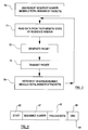
memory tag 30 operates as follows with reference toFigures 3 and 4 . When thetag 30 is moved sufficiently close to areader 31 so that inductive coupling can be established between theresonant circuit parts memory 34 to run theprogram 49. Theprogram 49, as shown atstep 70 ofFigure 3 , will read the sequence number stored insequence number register 48 and subtract one from that value, modulo the total number of packets. Atstep 71, thedata unit 46 identified by thesequence number 47 stored in theregister 48 will be read from thedata store 45 and transmitted as a part of a packet by operation of switch S1. A packet is generally illustrated at 64 inFigure 4 and comprises astart indicator 65, thesequence number 47, thedata unit 46 andvalidation information 66. In the present example thevalidation information 66 comprises a cyclic redundancy check of known type, which may preferably be simply generated when thedata unit 46 is read from thedata store 45. Alternatively, it might be envisaged that eachdata unit 46 be stored with its associated cyclic redundancy check, although it would use a potentially undesirable portion of the storage space available in thememory 34. It will be apparent that the validation data may be any other information as required, such as a check sum or other validation information. - At
step 72, thepacket 64 is generated, and atstep 73 transmitted to thereader 31. Theprogram 49 then increments the sequence number stored in thesequence number register 48 by one atstep 74 and then the method repeats fromstep 71. It will be apparent, that if theprogram 49 is not interrupted, it will continually cycle through the storeddata units 46 in the order specified by the sequence numbers 47. - The transmitted packet is received by the
reader 31 and the resultingoutput 60 is passed to thevalidation module 62 which performs a validation check on the receivedpacket 64 using thevalidation information 66. In the case where thevalidation information 66 comprises a cyclic redundancy check, this is performed by dividing the value of thepacket 64 by the predefined polynomial used to generate theCRC validation information 66. If the remainder is zero, the packet is valid and is passed tooutput 63. If the remainder is non-zero, there is an error in the packet and the packet should be discarded. - If there is an error in the packet, i.e. it is not valid, the
validation module 62 is then operable to control theamplitude modulator 61 to reduce the amplitude of the reader signal sufficiently so that insufficient power is received by thetag 30 to power thememory 34. Thevalidation module 62 then adjusts theamplitude modulator 61 to return the power in the reader signal to its previous level. Sufficient power will then be passed by therectifier 33 to thememory 34 for it to be powered, whereupon theprogram 49 will commence fromstep 70 atFigure 5 . The sequence number corresponding to the corrupt orinvalid packet 70 will be held in thesequence number register 48 in thenon-volatile memory 34. Atstep 70, theprogram 49 will thus decrement this value by one and then atsteps 71 to 73 generate a further signal comprising the data unit. The program 79 reads the data unit corresponding to the previous packet transmitted and sends it. Theprogram 49 then repeats thesteps 71 to 74 again to resend the data unit which was not received correctly and then succeeding packets. - In this manner, when an invalid packet is received from the
memory tag 30 it is not necessary to wait for the data carousel to return to the invalid packet in due course, nor is it necessary to transmit a specific request to thememory tag 30. By dropping the power supply to thememory tag 30 and then raising it again, thememory tag 30 is in effect caused to start re-transmitting data from that prior to the erroneous packet. Of course, the reader signal may be varied in any other way as desired. For example, by varying the frequency of the reader signal the strength of the resonant coupling between the reader and memory tag falls and so reduces the transfer of power to the memory tag. - The
validation module 62 or some other module may then be operable to generate a complete, sequential set ofdata units 46 by discarding packets which are received more than once and assembling the packets in order according to the sequence numbers 47. - It will be apparent that the
program 49 need not decrement the stored sequence number on power up, so that it starts transmitting the packet which was not validly received, or indeed may begin retransmission from earlier in the sequence by decrementing the stored sequence number by two or more. - In a preferred embodiment, the resonant frequency of the
resonant circuit parts frequency source 45 is about 2.45 GHz, and the resonant frequency of theresonant circuit part 32 is modulated by about 0.05 GHz either side of this reference frequency. At this frequency, component values for the inductors and the capacitors are small, allowing easy integration of the circuit and require relatively small areas of silicon on an integrated circuit. It is particularly desirable that thetag 30 be provided as an integrated circuit, for example as a CMOS integrated circuit. A schematic of such an integrated circuit is show at 80 inFigure 5 . The inductor L2 is shown at 35, here as an antenna coil having only a single turn although any number of turns may be provided as appropriate. The capacitor C4 is shown at 41, and the remaining components of the resonant circuit part and rectifyingcircuit part 33 are shown atblock 81. The memory is shown at 34. Thememory 34 provides 1Mbit of capacity of non-volatile memory and is of an area of approximately 1 mm2, and uses FRAM (ferroelectric random access memory) or MRAM (magnetoresistive random access memory) or similar memory technology requiring low power. Thememory tag 30 is of a substantially square shape in plan view with an external dimension D for the sides of around 1mm. - It will be apparent that the present invention may be used with any type of
memory tag 30 andreader 31 other than those disclosed herein. - In the present specification "comprises" means "includes or consists of" and "comprising" means "including or consisting of".
Claims (15)
- A memory tag (30) comprising a resonant circuit (32) part and a non-volatile memory (34),
the resonant circuit part (32) being arranged, in response to a reader signal received from a reader (31), to provide power to the memory (34),
the tag (30) being arranged to read the memory and transmit data stored in the memory (34) in response to the signal from the reader (31), and
wherein the data is stored in the memory in a plurality of data units (46), characterised in that each data unit (46) has an associated sequence number (47) stored in the memory,
the memory tag (30) being arranged to store the sequence number (47) of the data unit (46) to be transmitted in a register (48) in the non-volatile memory (34), and
when power is supplied to the memory (34), the stored sequence number (48) is decremented and the data units (46) are transmitted in sequence beginning with the data unit associated with the decremented sequence number (47). - A memory tag (30) according to claim 1 arranged to transmit the data unit (46) in a packet comprising validity information.
- A memory tag (30) according to claim 2 wherein the validity information comprises cyclic redundancy check data.
- A memory tag (30) according to claim 2 or claim 3 wherein the packet further comprises the sequence number (47) of the data unit (46).
- A memory tag (30) according to any one of the preceding claims arranged to read the stored sequence number (47), read the data unit (46) associated with the stored sequence number (47) transmit the data unit (46) and increment the stored sequence number (47).
- A reader (31) for reading a memory tag (30),
the reader (31) being arranged to transmit a reader signal to a memory tag (30) to supply power to a memory tag (30), and receive a signal comprising a data unit (46) and validity information, the data unit (46) having an associated sequence number, from a memory tag (30), characterised in that,
the reader (31) comprises
a validation module (62), the validation module (62) arranged to validate the received data unit (46) in accordance with the received validity information; and
an amplitude modulator (61), wherein the validation module (62) is arranged to control the amplitude modulator varying the reader signal to vary the power supplied to the memory tag (30) and decrement the associated sequence number if the data unit is not valid, and in that
the reader (31) is further arranged to receive a further signal comprising the data unit (46) associated with the decremented sequence number from the memory tag (30). - A reader according to claim 6 wherein the data unit (46) and the validity information is received in a packet.
- A reader according to claim 7 wherein the validity information comprises cyclic redundancy check information.
- A reader according to any one of claims 6 to 8 wherein the reader (31) is operable to store a plurality of received data units (46) in a sequence specified by the associated sequence numbers (47).
- A reader (31) according to anyone of claims 6 to 9 arrayed to vary the reader signal to vary the power supplied to the memory tag (30) by reducing the reader signal power such that the memory tag (30) is supplied with insufficient
power to operate and then increasing the reader signal power to supply power 30 to the memory tag (30). - An information retrieval system comprising a memory tag (30) according to any one of claims 1 to 5 and a reader according to any one of claims 6 to 10.
- A method of operating a memory tag (30) to transmit stored data, wherein the stored data comprises a plurality of data units, characterised in that,
the stored data further comprises a plurality of sequence numbers (47), each sequence number being associated with one of the data units,
the method comprising the initial step of, on supply of power to the memory tag (30),
reading a register (48) stored in a non-volatile memory (34) of the memory tag (30) which stores one of the sequence numbers (47),
decrementing the sequence number stored in the register, and transmitting the data units (46) in sequence beginning with the data unit (40) associated with the decremented sequence number. - A method according to claim 12, wherein the method further comprises repeating the steps of;
reading the register (48),
reading the data unit (46) associated with the stored sequence number (47) and transmitting the data unit (46) and
incrementing the sequence number (47) stored in the register (48). - A method according to claims 12 or 13 comprising transmitting validation information with the data unit.
- A method of operating a reader (31) for reading a memory tag (30) comprising transmitting a reader signal to a memory tag (30) to supply power to the memory tag (30), and
receiving a signal comprising a data unit (46) and validity information from a memory tag (30), the data unit (46) having an associated sequence number characterised in that the method further comprises,
validating the data unit (46) in accordance with the received validity information, and, if the data unit (46) is not valid,
varying the reader signal to vary the power supplied to the memory tag (30) and decrement the associated sequence number, and receiving a further signal comprising the data unit (46) associated with the decremented sequence number from the memory tag (30).
Applications Claiming Priority (2)
| Application Number | Priority Date | Filing Date | Title |
|---|---|---|---|
| GB0322694 | 2003-09-27 | ||
| GBGB0322694.1A GB0322694D0 (en) | 2003-09-27 | 2003-09-27 | A memory tag and a reader |
Publications (3)
| Publication Number | Publication Date |
|---|---|
| EP1519306A2 EP1519306A2 (en) | 2005-03-30 |
| EP1519306A3 EP1519306A3 (en) | 2006-03-15 |
| EP1519306B1 true EP1519306B1 (en) | 2011-06-29 |
Family
ID=29286980
Family Applications (1)
| Application Number | Title | Priority Date | Filing Date |
|---|---|---|---|
| EP04104692A Expired - Fee Related EP1519306B1 (en) | 2003-09-27 | 2004-09-27 | Memory tag and reader |
Country Status (4)
| Country | Link |
|---|---|
| US (1) | US7555616B2 (en) |
| EP (1) | EP1519306B1 (en) |
| JP (1) | JP4141998B2 (en) |
| GB (1) | GB0322694D0 (en) |
Families Citing this family (8)
| Publication number | Priority date | Publication date | Assignee | Title |
|---|---|---|---|---|
| US7818572B2 (en) | 2003-12-09 | 2010-10-19 | Dominic Kotab | Security system and method |
| FR2888976B1 (en) * | 2005-07-25 | 2007-10-12 | Oberthur Card Syst Sa | ELECTRONIC ENTITY WITH CONTACT AND REMOTE COMMUNICATION MEANS |
| US9727812B2 (en) * | 2007-07-23 | 2017-08-08 | Avery Dennison Retail Information Services, Llc | RFID device wtih control logic, and method |
| US7652578B2 (en) * | 2007-10-29 | 2010-01-26 | Motorola, Inc. | Detection apparatus and method for near field communication devices |
| CN107092950B (en) * | 2008-03-27 | 2021-04-09 | 环球生命科技咨询美国有限责任公司 | Gamma sterilizable RFID system to prevent unauthorized operation of associated disposable bioprocess components |
| EP2521072A1 (en) * | 2011-05-06 | 2012-11-07 | Gemalto SA | Radio communication device comprising an assisted radio source feed |
| CN103902940A (en) * | 2012-11-08 | 2014-07-02 | 冀京秋 | Self tester for integrated circuit sign |
| CN112799331B (en) * | 2021-01-26 | 2022-09-20 | 芜湖中科思萌特物联网科技有限公司 | Demodulation method of FPGA (field programmable Gate array) unfreezing program |
Family Cites Families (12)
| Publication number | Priority date | Publication date | Assignee | Title |
|---|---|---|---|---|
| US4818855A (en) * | 1985-01-11 | 1989-04-04 | Indala Corporation | Identification system |
| JPH03171384A (en) | 1989-11-30 | 1991-07-24 | Sony Corp | Information reader |
| JPH05250523A (en) | 1992-03-06 | 1993-09-28 | Toshiba Corp | Processing system |
| US5354975A (en) * | 1992-07-01 | 1994-10-11 | Tokimec Inc. | Contactless data processing apparatus |
| US5414833A (en) * | 1993-10-27 | 1995-05-09 | International Business Machines Corporation | Network security system and method using a parallel finite state machine adaptive active monitor and responder |
| JP3201157B2 (en) * | 1994-07-26 | 2001-08-20 | 松下電器産業株式会社 | IC card device |
| FR2741979B1 (en) * | 1995-12-01 | 1998-01-23 | Raimbault Pierre | METHOD FOR REMOTE QUERYING STATION LABELS AND LABEL FOR IMPLEMENTING SAME |
| US6404325B1 (en) * | 1998-01-08 | 2002-06-11 | Intermec Ip Corp. | Method and system for storage and recovery of vital information on radio frequency transponders |
| US6150948A (en) * | 1999-04-24 | 2000-11-21 | Soundcraft, Inc. | Low-power radio frequency identification reader |
| GB2363498B (en) | 2000-06-16 | 2005-06-01 | Marconi Caswell Ltd | Transponder device for generating a data bearing output |
| US6727803B2 (en) * | 2001-03-16 | 2004-04-27 | E-Tag Systems, Inc. | Method and apparatus for efficiently querying and identifying multiple items on a communication channel |
| GB2377341A (en) * | 2001-06-01 | 2003-01-08 | George L Powell | Signal sampling to reduce noise effects in an identification system |
-
2003
- 2003-09-27 GB GBGB0322694.1A patent/GB0322694D0/en not_active Ceased
-
2004
- 2004-09-23 US US10/947,171 patent/US7555616B2/en not_active Expired - Fee Related
- 2004-09-24 JP JP2004276699A patent/JP4141998B2/en not_active Expired - Fee Related
- 2004-09-27 EP EP04104692A patent/EP1519306B1/en not_active Expired - Fee Related
Also Published As
| Publication number | Publication date |
|---|---|
| US7555616B2 (en) | 2009-06-30 |
| EP1519306A3 (en) | 2006-03-15 |
| JP4141998B2 (en) | 2008-08-27 |
| JP2005108226A (en) | 2005-04-21 |
| US20050078498A1 (en) | 2005-04-14 |
| EP1519306A2 (en) | 2005-03-30 |
| GB0322694D0 (en) | 2003-10-29 |
Similar Documents
| Publication | Publication Date | Title |
|---|---|---|
| AU2009289470B2 (en) | Combination full-duplex and half-duplex electronic identification tag | |
| US5942977A (en) | Radio transponder | |
| US8248213B2 (en) | Deterministic method for efficiently querying and identifying multiple items on a communication channel | |
| US8193910B2 (en) | Interrogator, transponder and transponder identification method | |
| US9165170B1 (en) | RFID tag dynamically adjusting clock frequency | |
| US5550547A (en) | Multiple item radio frequency tag identification protocol | |
| US7893815B2 (en) | Method for selecting one or several transponders | |
| US7609147B2 (en) | Method and apparatus for improving wireless data transmission | |
| US7535359B2 (en) | Method of annotating an item with electronic data and apparatus therefor | |
| US20040201455A1 (en) | Method and apparatus for efficiently querying and identifying multiple items on a communication channel | |
| EP1387313A2 (en) | RFID-tag with tuning means and anticollision method | |
| US8193912B1 (en) | RFID tag dynamically adjusting clock frequency | |
| US8395525B2 (en) | Extending the read range of passive RFID tags | |
| US20070237087A1 (en) | Communication medium, communication medium processing apparatus, and communication medium processing system | |
| EP1519306B1 (en) | Memory tag and reader | |
| EP1998468A2 (en) | Multi-mode RFID reader Architecture | |
| CN102160314A (en) | Identification system | |
| EP1580903B1 (en) | Semiconductor device | |
| US20070120675A1 (en) | SSB response method of RFID tag | |
| Alma'aitah et al. | Modulation silencing: Novel RFID anti-collision resolution for passive tags |
Legal Events
| Date | Code | Title | Description |
|---|---|---|---|
| PUAI | Public reference made under article 153(3) epc to a published international application that has entered the european phase |
Free format text: ORIGINAL CODE: 0009012 |
|
| AK | Designated contracting states |
Kind code of ref document: A2 Designated state(s): AT BE BG CH CY CZ DE DK EE ES FI FR GB GR HU IE IT LI LU MC NL PL PT RO SE SI SK TR |
|
| AX | Request for extension of the european patent |
Extension state: AL HR LT LV MK |
|
| PUAL | Search report despatched |
Free format text: ORIGINAL CODE: 0009013 |
|
| AK | Designated contracting states |
Kind code of ref document: A3 Designated state(s): AT BE BG CH CY CZ DE DK EE ES FI FR GB GR HU IE IT LI LU MC NL PL PT RO SE SI SK TR |
|
| AX | Request for extension of the european patent |
Extension state: AL HR LT LV MK |
|
| 17P | Request for examination filed |
Effective date: 20060907 |
|
| 17Q | First examination report despatched |
Effective date: 20061004 |
|
| AKX | Designation fees paid |
Designated state(s): DE FR GB |
|
| GRAC | Information related to communication of intention to grant a patent modified |
Free format text: ORIGINAL CODE: EPIDOSCIGR1 |
|
| GRAP | Despatch of communication of intention to grant a patent |
Free format text: ORIGINAL CODE: EPIDOSNIGR1 |
|
| GRAS | Grant fee paid |
Free format text: ORIGINAL CODE: EPIDOSNIGR3 |
|
| GRAA | (expected) grant |
Free format text: ORIGINAL CODE: 0009210 |
|
| AK | Designated contracting states |
Kind code of ref document: B1 Designated state(s): DE FR GB |
|
| REG | Reference to a national code |
Ref country code: GB Ref legal event code: FG4D |
|
| REG | Reference to a national code |
Ref country code: DE Ref legal event code: R096 Ref document number: 602004033258 Country of ref document: DE Effective date: 20110818 |
|
| PLBE | No opposition filed within time limit |
Free format text: ORIGINAL CODE: 0009261 |
|
| STAA | Information on the status of an ep patent application or granted ep patent |
Free format text: STATUS: NO OPPOSITION FILED WITHIN TIME LIMIT |
|
| 26N | No opposition filed |
Effective date: 20120330 |
|
| REG | Reference to a national code |
Ref country code: DE Ref legal event code: R097 Ref document number: 602004033258 Country of ref document: DE Effective date: 20120330 |
|
| REG | Reference to a national code |
Ref country code: FR Ref legal event code: PLFP Year of fee payment: 13 |
|
| REG | Reference to a national code |
Ref country code: FR Ref legal event code: PLFP Year of fee payment: 14 |
|
| REG | Reference to a national code |
Ref country code: FR Ref legal event code: PLFP Year of fee payment: 15 |
|
| PGFP | Annual fee paid to national office [announced via postgrant information from national office to epo] |
Ref country code: GB Payment date: 20190820 Year of fee payment: 16 |
|
| PGFP | Annual fee paid to national office [announced via postgrant information from national office to epo] |
Ref country code: FR Payment date: 20191002 Year of fee payment: 17 |
|
| PGFP | Annual fee paid to national office [announced via postgrant information from national office to epo] |
Ref country code: DE Payment date: 20191004 Year of fee payment: 17 |
|
| GBPC | Gb: european patent ceased through non-payment of renewal fee |
Effective date: 20200927 |
|
| PG25 | Lapsed in a contracting state [announced via postgrant information from national office to epo] |
Ref country code: GB Free format text: LAPSE BECAUSE OF NON-PAYMENT OF DUE FEES Effective date: 20200927 |
|
| REG | Reference to a national code |
Ref country code: DE Ref legal event code: R119 Ref document number: 602004033258 Country of ref document: DE |
|
| PG25 | Lapsed in a contracting state [announced via postgrant information from national office to epo] |
Ref country code: FR Free format text: LAPSE BECAUSE OF NON-PAYMENT OF DUE FEES Effective date: 20210930 Ref country code: DE Free format text: LAPSE BECAUSE OF NON-PAYMENT OF DUE FEES Effective date: 20220401 |