EP1517381A2 - Semiconductor light emitting device and method of manufacturing the same - Google Patents
Semiconductor light emitting device and method of manufacturing the same Download PDFInfo
- Publication number
- EP1517381A2 EP1517381A2 EP04255596A EP04255596A EP1517381A2 EP 1517381 A2 EP1517381 A2 EP 1517381A2 EP 04255596 A EP04255596 A EP 04255596A EP 04255596 A EP04255596 A EP 04255596A EP 1517381 A2 EP1517381 A2 EP 1517381A2
- Authority
- EP
- European Patent Office
- Prior art keywords
- film
- semiconductor layer
- compound semiconductor
- metal compound
- type
- Prior art date
- Legal status (The legal status is an assumption and is not a legal conclusion. Google has not performed a legal analysis and makes no representation as to the accuracy of the status listed.)
- Granted
Links
Images



Classifications
-
- H—ELECTRICITY
- H10—SEMICONDUCTOR DEVICES; ELECTRIC SOLID-STATE DEVICES NOT OTHERWISE PROVIDED FOR
- H10H—INORGANIC LIGHT-EMITTING SEMICONDUCTOR DEVICES HAVING POTENTIAL BARRIERS
- H10H20/00—Individual inorganic light-emitting semiconductor devices having potential barriers, e.g. light-emitting diodes [LED]
- H10H20/80—Constructional details
- H10H20/83—Electrodes
- H10H20/832—Electrodes characterised by their material
- H10H20/835—Reflective materials
-
- H—ELECTRICITY
- H10—SEMICONDUCTOR DEVICES; ELECTRIC SOLID-STATE DEVICES NOT OTHERWISE PROVIDED FOR
- H10H—INORGANIC LIGHT-EMITTING SEMICONDUCTOR DEVICES HAVING POTENTIAL BARRIERS
- H10H20/00—Individual inorganic light-emitting semiconductor devices having potential barriers, e.g. light-emitting diodes [LED]
- H10H20/80—Constructional details
- H10H20/81—Bodies
- H10H20/822—Materials of the light-emitting regions
- H10H20/824—Materials of the light-emitting regions comprising only Group III-V materials, e.g. GaP
- H10H20/825—Materials of the light-emitting regions comprising only Group III-V materials, e.g. GaP containing nitrogen, e.g. GaN
Definitions
- the present invention relates to a light emitting device and a method of manufacturing the same, and more particularly, to a light emitting diode (LED) having a high emission efficiency, capable of operating at a low voltage and emitting blue and green lights, and a method of manufacturing the same.
- LED light emitting diode
- LEDs are widely used as a light source of an optical communication apparatus and a light source to visually display the operating state of an electronic apparatus. Accordingly, a variety of LEDs are provided according to the application fields of devices using LEDs. The range of use of LEDs has been further expanded by semiconductor devices emitting a blue light or a green light.
- FIG. 1 is an example of a conventional LED.
- an n-GaN layer 12 is formed on a substrate 10.
- the n-GaN layer 12 is divided into a first region R1, on which an active layer 14 is formed, and a second region R2, on which an n-type electrode 22 is formed. There is a step between the first and second regions R1 and R2.
- the active layer 14, a p-GaN layer 16, and a p-type electrode 18 are formed sequentially on the first region R1 of the n-GaN layer 12.
- the p-type electrode 18, as a high reflective electrode reflects the light emitted from the active layer 14 toward the substrate 10.
- the emission efficiency is low at a predetermined voltage.
- the problem of low emission efficiency could be solved by increasing the operating voltage.
- the LED comprising: at least an n-type compound semiconductor layer, an active layer, and a p-type compound semiconductor layer which are disposed between an n-type electrode layer and a p-type electrode layer, wherein the p-type electrode comprises first and second electrodes, each electrode having different characteristics of resistance and reflectance.
- the first electrode may be formed of a lanthanum nickel oxide film at a predetermined thickness.
- the second electrode may be formed of one selected from the group consisting of silver (Ag) film, aluminum (Al) film, rhodium (Rh) film, and tin (Sn) film.
- a LED comprising: a transparent substrate; an n-type compound semiconductor layer formed on the transparent substrate; an active layer formed on a first region of the n-type compound semiconductor layer; a p-type compound semiconductor layer formed on the active layer; a contact resistance reducing film formed on the p-type compound semiconductor layer; a p-type electrode formed on the contact resistance reducing film; and an n-type electrode formed on a second region separated from the first region of the n-type compound semiconductor layer.
- the contact resistance reducing film may be a lanthanum nickel oxide film.
- the p-type electrode may be formed of one selected from the group consisting of silver (Ag) film, aluminum (Al) film, rhodium (Rh) film, and tin (Sn) film.
- the present invention thus provides a LED capable of operating at a low operating voltage without reducing the emission efficiency, by lowering the contact resistance between a p-type electrode and a p-type compound layer, and a method of manufacturing the LED.
- a method of manufacturing a LED comprising: a first step of sequentially depositing an n-type compound semiconductor layer, an active layer, and a p-type compound semiconductor layer on a transparent substrate; a second step of exposing a predetermined portion of the n-type compound semiconductor layer by patterning sequentially the p-type compound semiconductor layer and the active layer; a third step of forming an n-type electrode on the disclosed region of the n-type compound semiconductor layer; a fourth step of forming a metal compound film on the patterned the p-type compound semiconductor layer; a fifth step of oxidizing the metal compound film; and a sixth step of forming a conductive reflection film on the oxidized metal compound film.
- the fourth step may comprise a step forming a photosensitive film pattern for disclosing the p-type compound semiconductor layer on the p-type compound semiconductor layer, and forming a metal compound film contacting the disclosed portion of the p-type compound semiconductor layer on the photosensitive film pattern.
- a resultant in which the reflective film is formed is annealed under a nitrogen atmosphere.
- a method for manufacturing a LED comprising: a first step of forming an n-type compound semiconductor layer on a transparent substrate; a second step of sequentially forming an active layer and a p-type compound semiconductor layer on the n-type compound semiconductor layer; a third step of patterning the p-type compound semiconductor layer and the active layer for exposing a predetermined portion of the n-type compound semiconductor layer; a fourth step of forming an n-type electrode on the exposed region of the n-type compound semiconductor layer; a fifth step of sequentially forming a metal compound film and a conductive reflection film on the patterned p-type compound semiconductor layer; and a sixth step of oxidizing the metal compound film.
- the fifth step may comprise: a step of forming a photosensitive film pattern for exposing the p-type compound semiconductor layer on the p-type compound semiconductor layer; a step of forming a metal compound film contacting the disclosed predetermined portion of the p-type compound semiconductor layer on the photosensitive film pattern, and a step of forming a reflective film on the metal compound.
- the photosensitive film pattern, together with the oxide of metal compound and the reflective film may be removed.
- the oxidized metal compound film may be annealed under a nitrogen atmosphere.
- a method of manufacturing a LED comprising: a first step of forming an n-type compound semiconductor layer, an active layer, a p-type compound semiconductor layer, a metal compound oxide film, and a conductive reflection film sequentially on a transparent substrate; a second step of sequentially exposing a predetermined portion of the n-type compound semiconductor layer by removing a predetermined portion of the conductive reflection film, the metal compound oxide film, the p-type compound semiconductor layer, and the active layer; and a third step of forming an n-type electrode on the exposed region of the n-type compound semiconductor layer.
- the first step may comprise: a step of sequentially forming the n-type compound semiconductor layer, the active layer, and the p-type compound semiconductor layer on the transparent substrate; a step of forming a metal compound film on the p-type compound semiconductor layer; a step of oxidizing the metal compound film; and a step of forming a reflective film on the oxidize the metal compound film.
- the first step may comprise: a step of sequentially forming the n-type compound semiconductor layer, the active layer, and the p-type compound semiconductor layer on the transparent substrate; a step of forming a metal compound film on the p-type compound semiconductor layer; a step of forming the reflective film on the metal compound film; and a step of oxidizing the metal compound film.
- the formed n-type electrode may be annealed under a nitrogen atmosphere.
- a method for manufacturing a LED comprising: a first step of sequentially forming an n-type compound semiconductor layer, an active layer, a p-type compound semiconductor layer, a metal compound film, and a conductive reflection film on a transparent substrate; a second step of exposing a predetermined portion of the n-type compound semiconductor layer by removing a predetermined portion of the conductive reflection film, the metal compound film, the p-type compound semiconductor layer, and the active layer; and a third step of oxidizing the metal compound film.
- an n-type electrode may be formed on the exposed region of the n-type compound semiconductor layer.
- the metal compound film may be formed of a lanthanum nikel film, and the metal compound oxide film may be a lanthanum nickel oxide film.
- the reflective film may be formed of one selected from the group consisting of silver film, aluminum film, rhodium film, and tin film.
- the present invention provides a material film between the reflective film used as a p- type electrode and the p-type compound semiconductor layer.
- the material film reduces the contact resistance between the reflective film and the p-type compound semiconductor layer and has a high reflectance. Accordingly, the present invention increases the efficiency at a lower operating voltage.
- a first compound semiconductor layer 42 is formed on a transparent substrate 40 of a LED according to the present invention.
- the first compound semiconductor layer 42 is preferably formed of an III-V group n-type semiconductor layer, for example, an n-GaN layer, but it can be formed of other semiconductor layers.
- the first compound semiconductor layer 42 is divided into a first region R1 and a second region R2.
- a second compound semiconductor layer 46 is deposited on the active layer 44.
- the second compound semiconductor layer 46 is preferably formed of an III-V group p-type compound semiconductor layer, for example, a p-GaN layer, but it may be formed of other semiconductor layers.
- a contact resistance reducing film 48, reducing a contact resistance and having a high reflectance, and a reflective film 50 are sequentially deposited on the second compound semiconductor layer 46.
- the contact resistance reducing film 48 and the reflective film 50 form a p-type electrode. It is considered that the reflective film 50 is used as the p-type electrode, and the contact resistance reducing film 48 is used as a means for reducing the contact resistance between the reflective film 50 and the second compound semiconductor layer 46.
- the contact resistance reducing film 48 may be formed of a compound containing a lanthanide, for example, a lanthanum (La) and a nickel (Ni), preferably, a lanthanum nickel oxide film, such as LaNiO 5 film.
- the thickness of the contact resistance reducing film 48 is in the range of 1 ⁇ 100 nm, preferably, approximately 10 nm.
- the reflective film 50 having a higher reflectance relative to the contact resistance reducing film 48 is preferably formed of silver (Ag), but it may be formed of other materials, such as one selected from the group cosisting of aluminum (Al), rhodium (Rh), and tin (Sn).
- An n-type electrode 52 is formed on the second region R2 of the first compound semiconductor layer 42.
- Light is emitted from the active layer 44 toward the transparent substrate 40 and the reflective film 50 by applying a required voltage, i.e., more than a threshold voltage to the p-type electrode, which is formed by the reflective film 50 or the reflective film 50 and the contact resistance reducing film 48, and the n-type electrode.
- the light L1 emitted toward the transparent substrate 40 is discharged through the transparent substrate 40.
- the light emitted toward the reflective film 50 is discharged through the transparent substrate 40 after being reflected by the contact resistance reducing film 48 or the reflective film 50.
- a reference numeral L2 represents the light reflected by the reflective film 50.
- the p-type electrode may be used as a p-type electrode of a light emitting device having p-type and n-type electrodes which face each other and of a light emitting device having a ridge wave guide.
- the n-type electrode 52 of FIG. 2 may be formed on the bottom of the transparent substrate 40 when the transparent substrate 40 is a conductive substrate.
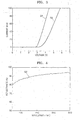
- FIG. 3 shows the characteristics of current versus voltage of a LED according to the present invention and the conventional art.
- a reference numeral G1 in FIG. 3 represents a first graph of current versus voltage of a p-type electrode formed of lanthanide nickel oxide film (LaNiO) and silver film (Ag) of a LED according to the present invention
- a numeral G2 represents a second graph of current versus voltage of a p-type electrode formed of silver (Ag) of a LED according to the conventional art.
- the LED according to the present invention commences operating at 3 volts, while, that of the conventional art commences operating at approximately 4 volts. That is, the operating voltage of the LED according to the present invention is reduced relative to the operating voltage of the conventional art by forming the p-type electrode with the contact resistance reducing film and the reflective film.
- FIG. 4 shows a reflection characteristic of the lanthanide nickel oxide film having a thickness of 10 nm used as the contact resistance reducing film 48 of a LED according to the present invention.
- a reference numeral G3 represents a third graph showing the reflection characteristic of the lanthanide nickel oxide film.
- the lanthanide nickel oxide film shows a high reflectance characteristic in all visible light range, for example, 85% in a short wavelength of 400 nm.
- the amount of light reflected to the transparent substrate 40 among the light discharged toward the reflective film 50 by the active layer 44 is increased compare to a case when there is no contact resistance reducing film 48.
- the amount of light discharged through the transparent substrate 40 of a LED according to the present invention is larger than that discharged through a reflective film 50 formed only by p-type electrode of the conventional art. That is, the emission efficiency of the present invention is higher than that of the conventional art at the same level of operating voltage.
- a LED according to the present invention is capable of operating at a lower voltage with a high light emission efficiency compared to a LED of the conventional art.
- a first compound semiconductor layer 42 is formed on a transparent substrate 40.
- the first compound semiconductor layer 42 is preferably formed of n-GaN layer, but it can be formed of other compound semiconductor layer.
- An active layer 44 and a second compound semiconductor layer 46 are formed sequentially on the first compound semiconductor layer 42.
- the second compound semiconductor layer 46 can be formed of p-GaN layer, but it can be formed of other compound semiconductor layer.
- a first photosensitive film pattern PR1 is formed on the second compound semiconductor layer 46.
- the first photosensitive film pattern PR1 defines regions for an n-type electrode and a p-type electrode, which will be later formed.
- the second compound semiconductor layer 46 and the active layer 44 are sequentially etched by using the first photosensitive film pattern PR1 as an etching mask.
- the etching can be done until the first compound semiconductor layer 42 is exposed, but it can be continued until a predetermined thickness of the first compound semiconductor layer 42 is removed.
- the first photosensitive film pattern PR1 is removed.
- An n-type electrode 52 is formed on the predetermined region where the exposed region by etching of the first compound semiconductor layer 42. The n-type electrode 52 can be formed after the following processes are completed.
- a second photosensitive film pattern PR2 is formed covering the whole region of the n-type electrode 52 formed including the n-type electrode 52, and exposing the majority of the second compound semiconductor layer 46.
- the second photosensitive film pattern PR2 defines a region for forming the p-type electrode.
- a metal compound film 47 is formed contacting the whole surface of the second compound semiconductor layer 46 on the second photosensitive film pattern PR2.
- the metal compound film 47 is preferably formed of lanthanide nickel compound (LaNi), but it can be formed of other metal compound film.
- the metal compound film 47 can have a thickness in the range of 1 ⁇ 100 nm, preferably, it is formed having a thickness of 10 nm.
- the metal compound film 47 may be formed differently depending on the film material used.
- the resultant metal compound film 47 is oxidized by annealing for a predetermined time at a predetermined temperature under an oxidizing atmosphere. Then, a contact resistance reducing film 48 contacting the whole surface of the disclosed region of the second compound semiconductor layer 46 is formed on the second photosensitive film pattern PR2 as depicted in FIG. 8.
- the contact resistance reducing film 48 as a high reflectance material film having a low electrical resistance as foregoing description, is preferably formed of lanthanide nickel oxide film, such as LaNiO 5 , but it can be formed of other oxide films.
- a reflective film 50 is formed on the contact resistance reducing film 48.
- the reflective film alone can be used as the p-type electrode, but the contact resistance reducing film 48 also can be used as an electrode considering the characteristic of resistance of the contact resistance reducing film 48. Therefore, the p-type electrode can be formed of both the reflective film 50 and the contact resistance reducing film 48.
- the reflective film 50 preferably can be formed of silver (Ag), but it can be formed of other materials having a high reflectance that can be used as an electrode, such as aluminum, rhodium, or tin.
- the second photosensitive film pattern PR2 is removed from the resulting product where the reflective film 50 is formed in FIG. 9.
- the contact resistance reducing film 48 and the reflective film 50 deposited sequentially on the second photosensitive film pattern PR2 are also removed.
- the contact resistance reducing film 48 and the reflective film 50 which will be used as the p-type electrode, are formed on the second compound semiconductor layer 46.
- a third photosensitive film pattern PR3 is formed covering the region of the n-type electrode 52 formed including the n-type electrode 52, and disclosing the majority of the second compound semiconductor layer 46.
- the third photosensitive film pattern PR3 defines a region for forming the p-type electrode.
- a metal compound film 47 and a reflective film 50 are formed sequentially on the third photosensitive film pattern PR3.
- the resulting product having the reflective film 50 is annealed to oxidize the metal compound film 47 as the same condition as described in the first embodiment under the oxidizing atmosphere.
- the metal compound film becomes a metal compound oxide film by annealing, and then a contact resistance reducing film 48 is formed between the reflective film 50 and the second compound semiconductor layer 46 as depicted in FIG. 12.
- the n-type electrode 52 can be formed after removing the third photosensitive film pattern PR3.
- a first compound semiconductor layer 42, the active layer 44, the second compound semiconductor layer 46, the metal compound film 47, and the reflective film 50 are sequentially deposited on the transparent substrate 40.
- a fourth photosensitive film pattern PR4 which defines the region for p-type electrode is formed on the reflective film 50.
- the deposited material films on the first compound semiconductor layer 42 are etched in reverse order by using the fourth photosensitive film pattern PR4 as an etching mask.
- the etching preferably can be done until the first compound semiconductor layer 42 is disclosed, but it can be continued until a predetermined thickness of the first compound semiconductor layer 42 is removed. A portion of the region of the first compound semiconductor layer 42 is disclosed by etching. An n-type electrode will be formed on the disclosed region of the first compound semiconductor layer 42 in the following process.
- the fourth photosensitive film pattern PR4 is removed by ashing and stripping.
- the resulting product is annealed as the same condition as described in the first embodiment under oxidizing atmosphere. Then, the metal compound film 47 is oxidized, and a contact resistance reducing film 48 is formed between the second compound semiconductor layer 46 and the reflective film 50.
- the fourth embodiment is characteristic in that, prior to forming the reflective film 50 on the metal compound film 47 as depicted in FIG.13 in the third embodiment, the oxidation of the metal compound 47 is performed in advance to form a metal compound film. After that, a fourth photosensitive film pattern PR4 is formed on the reflective film 50. By using the fourth photosensitive film pattern PR4 as an etching mask, the reflective film 50, the oxidized metal compound film, the second compound semiconductor layer 46, and the active layer 44 are etched sequentially. Then, the fourth photosensitive film pattern PR4 is removed.
- the resulting product can be heat treated under a nitrogen atmosphere.
- the heat treatment temperature can be in the range of 300 ⁇ 900 ⁇ for a predetermined time.
- the LED according to the present invention provides a material film having a low contacting resistance and a high reflectance formed between a reflective film, which is used as a p-type electrode, and a p-type compound semiconductor layer. Accordingly, the use of the LED according to the present invention allows operating at a low voltage and increasing the emission efficiency.
- the reflective film can be formed of double layers.
- the technical thought of the present invention can be applied to a LED having a p-type electrode and an n-type electrode formed not in a same direction.
- the oxidation process for converting a metal compound film to a contact resistance reducing film may adopt other method than annealing method.
- the present invention can be made in many different forms the scope of the present invention shall be defined by the sprit of technical thought with reference to the appended claims, not by the embodiments set forth herein.
Landscapes
- Led Devices (AREA)
- Electrodes Of Semiconductors (AREA)
Abstract
Description
Claims (25)
- A light emitting device comprising at least an n-type compound semiconductor layer, an active layer, and a p-type compound semiconductor layer which are disposed between an n-type electrode layer and a p-type electrode layer,
wherein the p-type electrode comprises first and second films, each electrode having a different resistance and reflectance. - The light emitting device of claim 1, wherein the first film is a lanthanum nickel oxide film having a predetermined thickness.
- The light emitting device of claim 1 or 2, wherein the second film is a film made of a material selected from the group consisting of silver (Ag), aluminum (Al), rhodium (Rh), and tin (Sn).
- A light emitting device according to claim 1, 2 or 3, further comprising a transparent substrate,
wherein the n-type compound semiconductor layer is formed on the transparent substrate;the active layer is formed on a first region of the n-type compound semiconductor layer;the p-type compound semiconductor layer is formed on the active layer;the first film is a contact resistance reducing film formed on the p-type compound semiconductor layer;the second film is formed on the contact resistance reducing film; andthe n-type electrode is formed on a second region separated from the first region of the n-type compound semiconductor layer. - A method of manufacturing a light emitting device, comprising:sequentially depositing an n-type compound semiconductor layer, an active layer, and a p-type compound semiconductor layer on a transparent substrate;exposing a predetermined portion of the n-type compound semiconductor layer by patterning sequentially the p-type compound semiconductor layer and the active layer;forming an n-type electrode on the exposed region of the n-type compound semiconductor layer;forming a metal compound film on the patterned p-type compound semiconductor layer;oxidizing the metal compound film; andforming a reflective film having a conductivity on the oxidized metal compound film.
- A method according to claim 5 including forming the reflective film after oxidizing the metal compound film.
- The method of claim 6, wherein the forming a metal compound comprising:forming a photosensitive film pattern for exposing the p-type compound semiconductor layer on the patterned p-type compound semiconductor layer; andforming a metal compound film contacting the exposed portion of the p-type compound semiconductor layer on the photosensitive film pattern.
- A method according to claim 5, including oxidizing the metal compound film after forming the reflective film.
- The method of claim 8, wherein the forming a metal compound film and a conductive reflection film comprisingforming a photosensitive film pattern for exposing the p-type compound semiconductor layer on the p-type compound semiconductor layer;forming a metal compound film contacting the exposed portion of the p-type compound semiconductor layer on the photosensitive film pattern; andforming a reflective film on the metal compound.
- The method of claim 9, wherein, after the oxidizing the metal compound film, the photosensitive film pattern together with the oxidized metal compound film and the reflective film are removed.
- The method of claim 9, wherein after oxidizing the metal compound film, a resultant in which the oxidized metal compound film is formed is annealed under nitrogen atmosphere.
- The method of any of claims 5 to 11, wherein the metal compound film is a lanthanum nickel film.
- The method of any of claims 5 to 12, wherein the reflective film is made of a material selected from the group consisting of silver (Ag), aluminum (Al), rhodium (Rh), and tin (Sn).
- The method of any of claims 5 to 13, wherein a resultant in which the reflective film is formed is annealed under a nitrogen atmosphere.
- A method of manufacturing a light emitting device, comprising:a first step, sequentially forming an n-type compound semiconductor layer, an active layer, a p-type compound semiconductor layer, a metal compound oxide film, and a conductive reflection film on a transparent substrate;a second step, exposing a predetermined portion of the n-type compound semiconductor layer by removing a predetermined portion of the conductive reflection film, the metal compound oxide film, the p-type compound semiconductor layer, and the active layer, sequentially; anda third step, forming an n-type electrode on the exposed region of the n-type compound semiconductor layer.
- The method of claim 15, wherein the first step comprises:sequentially forming the n-type compound semiconductor layer, the active layer, and the p-type compound semiconductor layer on the transparent substrate;forming a metal compound film on the p-type compound semiconductor layer;oxidizing the metal compound film; andforming the conductive reflection film on the oxidized metal compound film.
- The method of claim 15 or 16, wherein the first step comprises:sequentially forming the n-type compound semiconductor layer, the active layer, and the p-type compound semiconductor layer on the transparent substrate;forming a metal compound film on the p-type compound semiconductor layer;forming the conductive reflection film on the metal compound film; andoxidizing the metal compound film.
- The method of claim 15, 16 or 17, wherein the metal compound oxide film is a lanthanum nickel oxide film.
- The method of claim 15, 16, 17 or 18, wherein the conductive reflection film is formed of one selected from the group consisting of silver (Ag), aluminum (Al), rhodium (Rh), and tin (Sn).
- The method of any of claims 15 to 19, wherein a resultant in which the n-type electrode is formed is annealed under a nitrogen atmosphere.
- A method of manufacturing for a light emitting device, comprising:sequentially forming an n-type compound semiconductor layer, an active layer, a p-type compound semiconductor layer, a metal compound film, and a conductive reflection film on a transparent substrate;exposing a predetermined portion of the n-type compound semiconductor layer by removing a predetermined portion of the conductive reflection film, the metal compound film, the p-type compound semiconductor layer, and the active layer; andoxidizing the metal compound film.
- The method of claim 21, where after performing one of the exposing a predetermined portion of the n-type compound semiconductor layer and oxidizing the metal compound film, an n-type electrode is formed on the exposed region of the n-type compound semiconductor layer.
- The method of claim 21 or 22, the metal compound film is a lanthanum nickel film.
- The method of any of claims 21 to 23, where the conductive reflection film is formed of one selected from the group consisting of silver (Ag), aluminum (Al), rhodium (Rh), and tin (Sn).
- The method of any of claims 21 to 24, where after oxidizing the metal compound film, a resultant in which the oxidized metal compound film is formed is annealed under a nitrogen atmosphere.
Applications Claiming Priority (2)
| Application Number | Priority Date | Filing Date | Title |
|---|---|---|---|
| KR2003065219 | 2003-09-19 | ||
| KR1020030065219A KR100576849B1 (en) | 2003-09-19 | 2003-09-19 | Light emitting device and manufacturing method |
Publications (3)
| Publication Number | Publication Date |
|---|---|
| EP1517381A2 true EP1517381A2 (en) | 2005-03-23 |
| EP1517381A3 EP1517381A3 (en) | 2007-02-28 |
| EP1517381B1 EP1517381B1 (en) | 2009-06-10 |
Family
ID=34192251
Family Applications (1)
| Application Number | Title | Priority Date | Filing Date |
|---|---|---|---|
| EP04255596A Expired - Lifetime EP1517381B1 (en) | 2003-09-19 | 2004-09-15 | Semiconductor light emitting device |
Country Status (6)
| Country | Link |
|---|---|
| US (4) | US7115909B2 (en) |
| EP (1) | EP1517381B1 (en) |
| JP (1) | JP4535815B2 (en) |
| KR (1) | KR100576849B1 (en) |
| CN (1) | CN100505338C (en) |
| DE (1) | DE602004021460D1 (en) |
Families Citing this family (10)
| Publication number | Priority date | Publication date | Assignee | Title |
|---|---|---|---|---|
| KR100576849B1 (en) * | 2003-09-19 | 2006-05-10 | 삼성전기주식회사 | Light emitting device and manufacturing method |
| KR100638813B1 (en) * | 2005-04-15 | 2006-10-27 | 삼성전기주식회사 | Flip chip type nitride semiconductor light emitting device |
| TWI394290B (en) * | 2006-12-18 | 2013-04-21 | 台達電子工業股份有限公司 | Electroluminescent device and method of manufacturing same |
| JP2009049267A (en) * | 2007-08-22 | 2009-03-05 | Toshiba Corp | Semiconductor light emitting device and manufacturing method thereof |
| JP2010103500A (en) * | 2008-09-26 | 2010-05-06 | Toppan Printing Co Ltd | Organic electroluminescent element, method for manufacturing the same, image display unit and illuminating device |
| KR101248624B1 (en) | 2011-08-01 | 2013-03-28 | 주식회사 케이이씨 | Light emitting semiconductor device and manufacturing method thereof |
| KR101332686B1 (en) | 2012-07-11 | 2013-11-25 | 고려대학교 산학협력단 | Light emitting diode having transparent electrode |
| JP6024502B2 (en) * | 2013-02-13 | 2016-11-16 | 三菱マテリアル株式会社 | Composition for forming LaNiO3 thin film and method for forming LaNiO3 thin film using this composition |
| JP6627728B2 (en) * | 2016-11-24 | 2020-01-08 | 豊田合成株式会社 | Light emitting device manufacturing method |
| JP6841708B2 (en) * | 2017-03-31 | 2021-03-10 | ソウル バイオシス カンパニー リミテッドSeoul Viosys Co.,Ltd. | Light emitting element and manufacturing method of light emitting element |
Family Cites Families (50)
| Publication number | Priority date | Publication date | Assignee | Title |
|---|---|---|---|---|
| US4233148A (en) * | 1979-10-01 | 1980-11-11 | Great Lakes Carbon Corporation | Electrode composition |
| US4412895A (en) * | 1981-09-29 | 1983-11-01 | Westinghouse Electric Corp. | System using SO2 as an anode depolarizer in a solid oxide electrolyte electrolysis cell for H2 production from steam |
| EP0952617B1 (en) | 1993-04-28 | 2004-07-28 | Nichia Corporation | Gallium nitride-based III-V group compound semiconductor device |
| US5814533A (en) * | 1994-08-09 | 1998-09-29 | Rohm Co., Ltd. | Semiconductor light emitting element and manufacturing method therefor |
| JP3343030B2 (en) * | 1996-05-22 | 2002-11-11 | 日本碍子株式会社 | Sensor element |
| EP0957516A1 (en) * | 1996-08-20 | 1999-11-17 | Hitachi, Ltd. | Method for manufacturing oxide dielectric device, and memory and semiconductor device usign the device |
| EP2264794B1 (en) * | 1997-01-09 | 2014-11-19 | Nichia Corporation | Nitride semiconductor device |
| JP3462720B2 (en) * | 1997-07-16 | 2003-11-05 | 三洋電機株式会社 | N-type nitride semiconductor electrode, semiconductor element having the electrode, and method of manufacturing the same |
| US6078717A (en) * | 1997-07-22 | 2000-06-20 | Fuji Xerox Co., Ltd. | Opical waveguide device |
| US6015979A (en) * | 1997-08-29 | 2000-01-18 | Kabushiki Kaisha Toshiba | Nitride-based semiconductor element and method for manufacturing the same |
| WO1999025014A1 (en) * | 1997-11-10 | 1999-05-20 | Hitachi, Ltd. | Dielectric element and manufacturing method therefor |
| JP3589000B2 (en) * | 1997-12-26 | 2004-11-17 | 松下電器産業株式会社 | Gallium nitride based compound semiconductor light emitting device |
| US6841800B2 (en) * | 1997-12-26 | 2005-01-11 | Matsushita Electric Industrial Co., Ltd. | Light-emitting device comprising a gallium-nitride-group compound-semiconductor |
| US6296701B1 (en) * | 1998-09-30 | 2001-10-02 | Ut-Battelle, Llc | Method of depositing an electrically conductive oxide film on a textured metallic substrate and articles formed therefrom |
| JP3079262B2 (en) * | 1999-02-03 | 2000-08-21 | 工業技術院長 | Transparent conductive thin film and method for producing the same |
| JP2000305117A (en) * | 1999-02-19 | 2000-11-02 | Fuji Xerox Co Ltd | Optical device, method for driving optical device and production of optical device |
| WO2000063985A1 (en) * | 1999-04-20 | 2000-10-26 | Zinc Air Power Corporation | Lanthanum nickel compound/metal mixture as a third electrode in a metal-air battery |
| US6287947B1 (en) * | 1999-06-08 | 2001-09-11 | Lumileds Lighting, U.S. Llc | Method of forming transparent contacts to a p-type GaN layer |
| JP3127245B1 (en) * | 1999-09-03 | 2001-01-22 | 工業技術院長 | Multilayer electronic material, method of manufacturing the same, sensor and storage device using the same |
| US6573537B1 (en) | 1999-12-22 | 2003-06-03 | Lumileds Lighting, U.S., Llc | Highly reflective ohmic contacts to III-nitride flip-chip LEDs |
| PL202938B1 (en) * | 2000-02-16 | 2009-08-31 | Nichia Corp | Nitride semiconductor laser device |
| JP4024994B2 (en) * | 2000-06-30 | 2007-12-19 | 株式会社東芝 | Semiconductor light emitting device |
| US6727167B2 (en) * | 2000-10-13 | 2004-04-27 | Emcore Corporation | Method of making an aligned electrode on a semiconductor structure |
| US6649942B2 (en) * | 2001-05-23 | 2003-11-18 | Sanyo Electric Co., Ltd. | Nitride-based semiconductor light-emitting device |
| US20030016913A1 (en) * | 2001-07-20 | 2003-01-23 | Motorola, Inc. | Optical signal delay apparatus and methods |
| US20030016895A1 (en) * | 2001-07-23 | 2003-01-23 | Motorola, Inc. | Structure and method for fabricating semiconductor structures and devices utilizing photonic crystals |
| US6594414B2 (en) * | 2001-07-25 | 2003-07-15 | Motorola, Inc. | Structure and method of fabrication for an optical switch |
| US20030026515A1 (en) * | 2001-08-01 | 2003-02-06 | Motorola, Inc. | Monolithic tunable wavelength multiplexers and demultiplexers and methods for fabricating same |
| US20030047743A1 (en) * | 2001-09-04 | 2003-03-13 | Gang Li | Semiconductor light emitting device |
| TW512463B (en) * | 2001-09-28 | 2002-12-01 | Macronix Int Co Ltd | Method for epitaxial growth of lead zirconate titanate film |
| US6819540B2 (en) * | 2001-11-26 | 2004-11-16 | Shipley Company, L.L.C. | Dielectric structure |
| US6812496B2 (en) * | 2002-01-10 | 2004-11-02 | Sharp Kabushiki Kaisha | Group III nitride semiconductor laser device |
| US6885789B2 (en) * | 2002-06-07 | 2005-04-26 | Fujitsu Limited | Optical switch fabricated by a thin film process |
| SG115549A1 (en) * | 2002-07-08 | 2005-10-28 | Sumitomo Chemical Co | Epitaxial substrate for compound semiconductor light emitting device, method for producing the same and light emitting device |
| US7048844B2 (en) * | 2002-11-15 | 2006-05-23 | Delphi Technologies, Inc. | Gas sensor and method for use thereof |
| KR100495215B1 (en) * | 2002-12-27 | 2005-06-14 | 삼성전기주식회사 | VERTICAL GaN LIGHT EMITTING DIODE AND METHOD OF PRODUCING THE SAME |
| US6876536B2 (en) * | 2002-12-27 | 2005-04-05 | Tdk Corporation | Thin film capacitor and method for fabricating the same |
| US6861800B2 (en) * | 2003-02-18 | 2005-03-01 | Eastman Kodak Company | Tuned microcavity color OLED display |
| US6958900B2 (en) * | 2003-02-26 | 2005-10-25 | Tdk Corporation | Multi-layered unit including electrode and dielectric layer |
| US7067458B2 (en) * | 2003-02-26 | 2006-06-27 | Tdk Corporation | Multi-layered unit including electrode and dielectric layer |
| US6788522B1 (en) * | 2003-02-26 | 2004-09-07 | Tdk Corporation | Multi-layered unit including electrode and dielectric layer |
| US6977806B1 (en) * | 2003-02-26 | 2005-12-20 | Tdk Corporation | Multi-layered unit including electrode and dielectric layer |
| US6891714B2 (en) * | 2003-02-26 | 2005-05-10 | Tdk Corporation | Multi-layered unit including electrode and dielectric layer |
| US20040164416A1 (en) * | 2003-02-26 | 2004-08-26 | Tdk Corporation | Multi-layered unit |
| JP4136746B2 (en) * | 2003-03-25 | 2008-08-20 | 三洋電機株式会社 | Method of forming nitride semiconductor and nitride semiconductor device |
| US6930875B2 (en) * | 2003-06-12 | 2005-08-16 | Tdk Corporation | Multi-layered unit |
| KR100561840B1 (en) * | 2003-07-09 | 2006-03-16 | 삼성전자주식회사 | Electrode layer, light emitting device and electrode layer manufacturing method including the same |
| KR100576849B1 (en) * | 2003-09-19 | 2006-05-10 | 삼성전기주식회사 | Light emitting device and manufacturing method |
| KR100580634B1 (en) * | 2003-12-24 | 2006-05-16 | 삼성전자주식회사 | Nitride-based light emitting device and its manufacturing method |
| TWI331816B (en) * | 2007-04-03 | 2010-10-11 | Advanced Optoelectronic Tech | Semiconductor light-emitting device |
-
2003
- 2003-09-19 KR KR1020030065219A patent/KR100576849B1/en not_active Expired - Fee Related
-
2004
- 2004-09-15 US US10/940,748 patent/US7115909B2/en not_active Expired - Fee Related
- 2004-09-15 EP EP04255596A patent/EP1517381B1/en not_active Expired - Lifetime
- 2004-09-15 DE DE602004021460T patent/DE602004021460D1/en not_active Expired - Lifetime
- 2004-09-17 JP JP2004272043A patent/JP4535815B2/en not_active Expired - Fee Related
- 2004-09-20 CN CNB2004100825462A patent/CN100505338C/en not_active Expired - Fee Related
-
2006
- 2006-08-21 US US11/506,837 patent/US7790486B2/en not_active Expired - Fee Related
-
2010
- 2010-07-23 US US12/842,096 patent/US20100285622A1/en not_active Abandoned
-
2012
- 2012-04-03 US US13/438,323 patent/US8435813B2/en not_active Expired - Fee Related
Also Published As
| Publication number | Publication date |
|---|---|
| DE602004021460D1 (en) | 2009-07-23 |
| US20120190142A1 (en) | 2012-07-26 |
| EP1517381B1 (en) | 2009-06-10 |
| US20050062051A1 (en) | 2005-03-24 |
| EP1517381A3 (en) | 2007-02-28 |
| US8435813B2 (en) | 2013-05-07 |
| US20060281209A1 (en) | 2006-12-14 |
| US20100285622A1 (en) | 2010-11-11 |
| JP2005094020A (en) | 2005-04-07 |
| CN100505338C (en) | 2009-06-24 |
| US7790486B2 (en) | 2010-09-07 |
| US7115909B2 (en) | 2006-10-03 |
| KR100576849B1 (en) | 2006-05-10 |
| KR20050028706A (en) | 2005-03-23 |
| CN1599088A (en) | 2005-03-23 |
| JP4535815B2 (en) | 2010-09-01 |
Similar Documents
| Publication | Publication Date | Title |
|---|---|---|
| US8435813B2 (en) | Light emitting device and method of manufacturing the same | |
| EP1810351B1 (en) | Gan compound semiconductor light emitting element | |
| EP1709695B1 (en) | Gallium nitride-based iii-v group compound semiconductor device and method of manufacturing the same | |
| US5760423A (en) | Semiconductor light emitting device, electrode of the same device and method of manufacturing the same device | |
| JP5128755B2 (en) | III-V group GaN compound semiconductor and p-type electrode applied thereto | |
| KR100670928B1 (en) | HA-based compound semiconductor light emitting device and method of manufacturing the same | |
| KR20010029787A (en) | METHOD OF FORMING TRANSPARENT CONTACTS TO A P-TYPE GaN LAYER | |
| JP2003133590A (en) | Gallium nitride based compound semiconductor light emitting device and method of manufacturing the same | |
| USRE43426E1 (en) | Fabrication method of transparent electrode on visible light-emitting diode | |
| US11239392B2 (en) | Optoelectronic semiconductor chip, high-voltage semiconductor chip and method for producing an optoelectronic semiconductor chip | |
| CN100442549C (en) | GaN-based III-V compound semiconductor light-emitting device and manufacturing method thereof | |
| JP2005223326A (en) | ELECTRODE LAYER, LIGHT EMITTING DEVICE HAVING SAME, AND METHOD FOR PRODUCING ELECTRODE LAYER | |
| JP5130436B2 (en) | GaN-based semiconductor light-emitting device and manufacturing method thereof | |
| CN109860349B (en) | LED chip and manufacturing method thereof | |
| CN100391013C (en) | Method for manufacturing gallium nitride semiconductor light emitting device | |
| US6174747B1 (en) | Method of fabricating ridge waveguide semiconductor light-emitting device | |
| JP2002016286A (en) | Semiconductor light emitting device | |
| JP2916424B2 (en) | Semiconductor light emitting device, electrode of semiconductor light emitting device, and method of manufacturing semiconductor light emitting device | |
| US20240097075A1 (en) | Method for manufacturing light-emitting element and light-emitting element | |
| JP2014060335A (en) | Method of manufacturing semiconductor light-emitting element | |
| KR20050072521A (en) | A low-resistance electrode of compound semiconductor light emitting device and a compound semiconductor light emitting device using the electrode | |
| KR20140093340A (en) | Forming method of current blocking layer and manufacturing method of led using the same |
Legal Events
| Date | Code | Title | Description |
|---|---|---|---|
| PUAI | Public reference made under article 153(3) epc to a published international application that has entered the european phase |
Free format text: ORIGINAL CODE: 0009012 |
|
| AK | Designated contracting states |
Kind code of ref document: A2 Designated state(s): AT BE BG CH CY CZ DE DK EE ES FI FR GB GR HU IE IT LI LU MC NL PL PT RO SE SI SK TR |
|
| AX | Request for extension of the european patent |
Extension state: AL HR LT LV MK |
|
| PUAL | Search report despatched |
Free format text: ORIGINAL CODE: 0009013 |
|
| AK | Designated contracting states |
Kind code of ref document: A3 Designated state(s): AT BE BG CH CY CZ DE DK EE ES FI FR GB GR HU IE IT LI LU MC NL PL PT RO SE SI SK TR |
|
| AX | Request for extension of the european patent |
Extension state: AL HR LT LV MK |
|
| 17P | Request for examination filed |
Effective date: 20070613 |
|
| 17Q | First examination report despatched |
Effective date: 20070807 |
|
| AKX | Designation fees paid |
Designated state(s): DE NL |
|
| GRAP | Despatch of communication of intention to grant a patent |
Free format text: ORIGINAL CODE: EPIDOSNIGR1 |
|
| RTI1 | Title (correction) |
Free format text: SEMICONDUCTOR LIGHT EMITTING DEVICE |
|
| GRAS | Grant fee paid |
Free format text: ORIGINAL CODE: EPIDOSNIGR3 |
|
| GRAA | (expected) grant |
Free format text: ORIGINAL CODE: 0009210 |
|
| AK | Designated contracting states |
Kind code of ref document: B1 Designated state(s): DE NL |
|
| REF | Corresponds to: |
Ref document number: 602004021460 Country of ref document: DE Date of ref document: 20090723 Kind code of ref document: P |
|
| PLBE | No opposition filed within time limit |
Free format text: ORIGINAL CODE: 0009261 |
|
| STAA | Information on the status of an ep patent application or granted ep patent |
Free format text: STATUS: NO OPPOSITION FILED WITHIN TIME LIMIT |
|
| 26N | No opposition filed |
Effective date: 20100311 |
|
| REG | Reference to a national code |
Ref country code: NL Ref legal event code: SD Effective date: 20100521 |
|
| REG | Reference to a national code |
Ref country code: DE Ref legal event code: R081 Ref document number: 602004021460 Country of ref document: DE Owner name: SAMSUNG ELECTRONICS CO., LTD., SUWON-SI, KR Free format text: FORMER OWNER: SAMSUNG ELECTRO-MECHANICS CO., LTD., SUWON, KYONGGI, KR Effective date: 20110228 |
|
| REG | Reference to a national code |
Ref country code: DE Ref legal event code: R082 Ref document number: 602004021460 Country of ref document: DE Representative=s name: GRUENECKER, KINKELDEY, STOCKMAIR & SCHWANHAEUS, DE |
|
| REG | Reference to a national code |
Ref country code: DE Ref legal event code: R082 Ref document number: 602004021460 Country of ref document: DE Representative=s name: GRUENECKER, KINKELDEY, STOCKMAIR & SCHWANHAEUS, DE Effective date: 20121204 Ref country code: DE Ref legal event code: R081 Ref document number: 602004021460 Country of ref document: DE Owner name: SAMSUNG ELECTRONICS CO., LTD., KR Free format text: FORMER OWNER: SAMSUNG LED CO.,LTD., SUWON, KR Effective date: 20121204 Ref country code: DE Ref legal event code: R081 Ref document number: 602004021460 Country of ref document: DE Owner name: SAMSUNG ELECTRONICS CO., LTD., SUWON-SI, KR Free format text: FORMER OWNER: SAMSUNG LED CO.,LTD., SUWON, KYONGGI, KR Effective date: 20121204 Ref country code: DE Ref legal event code: R082 Ref document number: 602004021460 Country of ref document: DE Representative=s name: GRUENECKER PATENT- UND RECHTSANWAELTE PARTG MB, DE Effective date: 20121204 |
|
| REG | Reference to a national code |
Ref country code: NL Ref legal event code: SD Effective date: 20130620 |
|
| PGFP | Annual fee paid to national office [announced via postgrant information from national office to epo] |
Ref country code: NL Payment date: 20130822 Year of fee payment: 10 Ref country code: DE Payment date: 20130820 Year of fee payment: 10 |
|
| REG | Reference to a national code |
Ref country code: DE Ref legal event code: R119 Ref document number: 602004021460 Country of ref document: DE |
|
| REG | Reference to a national code |
Ref country code: DE Ref legal event code: R119 Ref document number: 602004021460 Country of ref document: DE Effective date: 20150401 |
|
| PG25 | Lapsed in a contracting state [announced via postgrant information from national office to epo] |
Ref country code: NL Free format text: LAPSE BECAUSE OF NON-PAYMENT OF DUE FEES Effective date: 20150401 |
|
| PG25 | Lapsed in a contracting state [announced via postgrant information from national office to epo] |
Ref country code: DE Free format text: LAPSE BECAUSE OF NON-PAYMENT OF DUE FEES Effective date: 20150401 |