EP1517189A2 - Critical dimension optimisation in lithography - Google Patents

Critical dimension optimisation in lithography Download PDF

Info

Publication number
EP1517189A2
EP1517189A2 EP04255674A EP04255674A EP1517189A2 EP 1517189 A2 EP1517189 A2 EP 1517189A2 EP 04255674 A EP04255674 A EP 04255674A EP 04255674 A EP04255674 A EP 04255674A EP 1517189 A2 EP1517189 A2 EP 1517189A2
Authority
EP
European Patent Office
Prior art keywords
exposure
substrates
substrate
attributes
corrective
Prior art date
Legal status (The legal status is an assumption and is not a legal conclusion. Google has not performed a legal analysis and makes no representation as to the accuracy of the status listed.)
Withdrawn
Application number
EP04255674A
Other languages
German (de)
French (fr)
Other versions
EP1517189A3 (en
Inventor
Todd David Hiar
Wim Tijibbo Tel
Todd J. David
Theodore Allen Paxton
Current Assignee (The listed assignees may be inaccurate. Google has not performed a legal analysis and makes no representation or warranty as to the accuracy of the list.)
ASML Netherlands BV
Original Assignee
ASML Netherlands BV
Priority date (The priority date is an assumption and is not a legal conclusion. Google has not performed a legal analysis and makes no representation as to the accuracy of the date listed.)
Filing date
Publication date
Application filed by ASML Netherlands BV filed Critical ASML Netherlands BV
Publication of EP1517189A2 publication Critical patent/EP1517189A2/en
Publication of EP1517189A3 publication Critical patent/EP1517189A3/en
Withdrawn legal-status Critical Current

Links

Images

Classifications

    • GPHYSICS
    • G03PHOTOGRAPHY; CINEMATOGRAPHY; ANALOGOUS TECHNIQUES USING WAVES OTHER THAN OPTICAL WAVES; ELECTROGRAPHY; HOLOGRAPHY
    • G03FPHOTOMECHANICAL PRODUCTION OF TEXTURED OR PATTERNED SURFACES, e.g. FOR PRINTING, FOR PROCESSING OF SEMICONDUCTOR DEVICES; MATERIALS THEREFOR; ORIGINALS THEREFOR; APPARATUS SPECIALLY ADAPTED THEREFOR
    • G03F7/00Photomechanical, e.g. photolithographic, production of textured or patterned surfaces, e.g. printing surfaces; Materials therefor, e.g. comprising photoresists; Apparatus specially adapted therefor
    • G03F7/70Microphotolithographic exposure; Apparatus therefor
    • G03F7/708Construction of apparatus, e.g. environment aspects, hygiene aspects or materials
    • G03F7/70991Connection with other apparatus, e.g. multiple exposure stations, particular arrangement of exposure apparatus and pre-exposure and/or post-exposure apparatus; Shared apparatus, e.g. having shared radiation source, shared mask or workpiece stage, shared base-plate; Utilities, e.g. cable, pipe or wireless arrangements for data, power, fluids or vacuum
    • GPHYSICS
    • G03PHOTOGRAPHY; CINEMATOGRAPHY; ANALOGOUS TECHNIQUES USING WAVES OTHER THAN OPTICAL WAVES; ELECTROGRAPHY; HOLOGRAPHY
    • G03FPHOTOMECHANICAL PRODUCTION OF TEXTURED OR PATTERNED SURFACES, e.g. FOR PRINTING, FOR PROCESSING OF SEMICONDUCTOR DEVICES; MATERIALS THEREFOR; ORIGINALS THEREFOR; APPARATUS SPECIALLY ADAPTED THEREFOR
    • G03F7/00Photomechanical, e.g. photolithographic, production of textured or patterned surfaces, e.g. printing surfaces; Materials therefor, e.g. comprising photoresists; Apparatus specially adapted therefor
    • G03F7/70Microphotolithographic exposure; Apparatus therefor
    • G03F7/70483Information management; Active and passive control; Testing; Wafer monitoring, e.g. pattern monitoring
    • G03F7/70491Information management, e.g. software; Active and passive control, e.g. details of controlling exposure processes or exposure tool monitoring processes
    • G03F7/705Modelling or simulating from physical phenomena up to complete wafer processes or whole workflow in wafer productions
    • GPHYSICS
    • G03PHOTOGRAPHY; CINEMATOGRAPHY; ANALOGOUS TECHNIQUES USING WAVES OTHER THAN OPTICAL WAVES; ELECTROGRAPHY; HOLOGRAPHY
    • G03FPHOTOMECHANICAL PRODUCTION OF TEXTURED OR PATTERNED SURFACES, e.g. FOR PRINTING, FOR PROCESSING OF SEMICONDUCTOR DEVICES; MATERIALS THEREFOR; ORIGINALS THEREFOR; APPARATUS SPECIALLY ADAPTED THEREFOR
    • G03F7/00Photomechanical, e.g. photolithographic, production of textured or patterned surfaces, e.g. printing surfaces; Materials therefor, e.g. comprising photoresists; Apparatus specially adapted therefor
    • G03F7/70Microphotolithographic exposure; Apparatus therefor
    • G03F7/70483Information management; Active and passive control; Testing; Wafer monitoring, e.g. pattern monitoring
    • G03F7/7055Exposure light control in all parts of the microlithographic apparatus, e.g. pulse length control or light interruption
    • G03F7/70558Dose control, i.e. achievement of a desired dose
    • GPHYSICS
    • G03PHOTOGRAPHY; CINEMATOGRAPHY; ANALOGOUS TECHNIQUES USING WAVES OTHER THAN OPTICAL WAVES; ELECTROGRAPHY; HOLOGRAPHY
    • G03FPHOTOMECHANICAL PRODUCTION OF TEXTURED OR PATTERNED SURFACES, e.g. FOR PRINTING, FOR PROCESSING OF SEMICONDUCTOR DEVICES; MATERIALS THEREFOR; ORIGINALS THEREFOR; APPARATUS SPECIALLY ADAPTED THEREFOR
    • G03F7/00Photomechanical, e.g. photolithographic, production of textured or patterned surfaces, e.g. printing surfaces; Materials therefor, e.g. comprising photoresists; Apparatus specially adapted therefor
    • G03F7/70Microphotolithographic exposure; Apparatus therefor
    • G03F7/70483Information management; Active and passive control; Testing; Wafer monitoring, e.g. pattern monitoring
    • G03F7/70605Workpiece metrology
    • G03F7/70616Monitoring the printed patterns
    • G03F7/70625Dimensions, e.g. line width, critical dimension [CD], profile, sidewall angle or edge roughness

Abstract

A system, apparatus, and method for improving CD uniformity in lithographic system, is presented herein. The system includes an exposure apparatus (102) configured to expose substrates, a track apparatus (104) that is operatively coupled to the exposure apparatus and a plurality of processing modules and apparatus. The system also includes a measuring device configured to measure attributes of the exposed and processed substrates and to assess whether the exposed and processed substrate attributes are uniform based on pre-specified substrate profile information. The system further includes a module configured to adaptively calculate corrective exposure data based on the measured attributes upon determining that said attributes are not uniform. The corrective exposure data is configured to correct for nonuniformities in the substrates by regulating the exposure dosage of the exposure apparatus. Once the substrates are assessed to achieve the desired uniformity, the substrates are exposed by the exposure apparatus in accordance with the corrective exposure data, the uniformity of the exposed substrate continues to be monitored and the dose corrections are updated as required to maintain uniformity.
Figure 00000001

Description

    BACKGROUND OF THE INVENTION
  • The present invention generally relates to lithographic systems and methods of lithographic exposure.
  • The term "patterning device" as will be employed herein should be broadly interpreted to refer to devices that can be used to endow an incoming radiation beam with a patterned cross-section, corresponding to a pattern that is to be created in a target portion of the substrate. The term "light valve" may also be used in this context. Generally, the pattern will correspond to a particular functional layer in a device being created in the target portion, such as an integrated circuit or other device (see below). Examples of such patterning devices include:
  • (a) a mask: the concept of a mask is well known in lithography, and it includes mask types such as binary, alternating phase-shift, and attenuated phase-shift, as well as various hybrid mask types. Placement of such a mask in the radiation beam causes selective transmission (in the case of a transmissive mask) or reflection (in the case of a reflective mask) of the radiation impinging on the mask, according to the pattern on the mask. In the case of a mask, the support structure will generally be a mask table, which ensures that the mask can be held at a desired position in the incoming radiation beam, and that it can be moved relative to the beam if so desired;
  • (b) a programmable mirror array: an example of such a device is a matrix-addressable surface having a viscoelastic control layer and a reflective surface. The basic principle behind such an apparatus is that (for example) addressed areas of the reflective surface reflect incident light as diffracted light, whereas unaddressed areas reflect incident light as undiffracted light. Using an appropriate filter, the said undiffracted light can be filtered out of the reflected beam, leaving only the diffracted light behind; in this manner, the beam becomes patterned according to the addressing pattern of the matrix-addressable surface. The required matrix addressing can be performed using suitable electronic means. More information on such mirror arrays can be gleaned, for example, from United States Patent Nos. US 5,296,891 and US 5,523,193, which are incorporated herein by reference. In the case of a programmable mirror array, the said support structure may be embodied as a frame or table, for example, which may be fixed or movable as required; and
  • (c) a programmable LCD array: an example of such a construction is given in United States Patent No. US 5,229,872, which is incorporated herein by reference. As above, the support structure in this case may be embodied as a frame or table, for example, which may be fixed or movable as required.
  • For purposes of simplicity, the rest of this text may, at certain locations, specifically direct itself to examples involving a mask and mask table; however, the general principles discussed in such instances should be seen in the broader context of the patterning devices as set forth above. Also, the projection system may hereinafter be referred to as the "lens"; however, this term should be broadly interpreted as encompassing various types of projection system, including refractive optics, reflective optics, and catadioptric systems, for example. The radiation system may also include components operating according to any of these design types for directing, shaping or controlling the projection beam of radiation, and such components may also be referred to below, collectively or singularly, as a "lens".
  • Lithographic exposure apparatuses can be used, for example, in the manufacture of integrated circuits (ICs). In such a case, the patterning devices may generate a circuit pattern corresponding to an individual layer of the IC, and this pattern can be imaged onto a target portion (e.g. comprising one or more dies) on a substrate (silicon wafer) that has been coated with a layer of radiation-sensitive material (resist). In general, a single wafer will contain a whole network of adjacent target portions that are successively irradiated via the projection system, one at a time.
  • In current apparatuses, employing patterning by a mask on a mask table, a distinction can be made between two different types of machine. In one type of lithographic exposure apparatus, each target portion is irradiated by exposing the entire mask pattern onto the target portion in one go; such an apparatus is commonly referred to as a wafer stepper. In an alternative apparatus - commonly referred to as a step-and-scan apparatus - each target portion is irradiated by progressively scanning the mask pattern under the projection beam in a given reference direction (the "scanning" direction) while synchronously scanning the substrate table parallel or anti-parallel to this direction. Because, in general, the projection system will have a magnification factor M (generally < 1), the speed V at which the substrate table is scanned will be a factor M times that at which the mask table is scanned. More information with regard to lithographic devices as here described can be gleaned, for example, from United States Patent No. 6,046,792, incorporated herein by reference.
  • It is to be noted that the lithographic apparatus may also be of a type having two or more substrate tables (and/or two or more mask tables). In such "multiple stage" devices the additional tables may be used in parallel, or preparatory steps may be carried out on one or more tables while one or more other tables are being used for exposures. Twin stage lithographic apparatus are described, for example, in United States Patent No. 5,969,441 and WO 98/40791, incorporated herein by reference.
  • Among other things, lithographic systems are used in the manufacture of integrated circuits (ICs). Such systems commonly employ a lithographic exposure apparatus and a wafer track apparatus. The lithographic exposure apparatus is configured to project or expose circuit pattern residing on a reticle (e.g., mask) onto a target field of a silicon wafer substrate layer via an irradiating projection beam. The projection beam may encompass different types of electromagnetic radiation including, but not limited to, ultraviolet radiation (UV) and extreme ultra-violet radiation (EUV), as well as particle beams, such as ion beams or electron beams.
  • Generally, the silicon wafer layer is previously coated with radiation-sensitive material (e.g., resist) that interacts with the impinging projection beam to replicate the profile and features of the mask circuit pattern onto the wafer substrate target fields. In general, a single wafer layer will contain a entire network of adjacent target fields that are successively irradiated.
  • Current lithographic exposure apparatuses fall into two general categories: stepper tools and step-and-scan tools. In steppers, each target portion is irradiated by exposing the entire mask pattern onto the target portion at once. In step-and-scan tools, each target portion is irradiated by progressively scanning the mask circuit pattern under the projection beam in a given reference direction while synchronously scanning the substrate.
  • Irrespective of the tool used, the substrate may be subjected to a variety of processes before the exposure process. For example, as indicated above, the substrate will generally be treated with resist before exposure. Also, prior to exposure, the substrate may be subjected to cleaning, etching, ion implantation (e.g., doping), metallization, oxidation, chemo-mechanical polishing, priming, resist coating, soft bake processes, , and measurement processes.
  • The substrate may also be subjected to a series of post-exposure processes, such as, for example, post exposure bake (PEB), development, hard bake, etching, ion implantation (e.g., doping), metallization, oxidation, chemo-mechanical polishing, cleaning, and measurement processes. And, if several layers are required, which is usually the case, the entire procedure, or variants thereof, will have to be repeated for each new layer.
  • These pre- and post-exposure processes are performed by stations or modules designed for their respective purposes. The substrate is subjected to these processing modules, as well as to the lithographic exposure apparatus, in a pre-defined sequence. In this arrangement, the substrate wafers travel in a pre-specified processing path to get serviced by specific processing modules that can be tracked. The processing path can be monitored, recorded, controlled, and limited to specific paths.
  • As indicated in FIG. 1A, which schematically depicts lithographic system 100, wafer track apparatus 104 interconnects lithographic exposure apparatus 102 with a serie of pre-processing modules 104, 106 and post exposure processing modules 104, 108. The pre- and post-exposure processing modules 104, 106, 108 can be apparatus that are external to the wafer track apparatus or modules that are internal to the wafer track apparatus. To accommodate the transfer of substrates between these processing steps the wafer track apparatus 104 may also include interface sections configured to transport the wafer substrates to and from lithographic exposure apparatus 102, pre-processing apparatus 106, post-processing apparatus 108, and transport the wafer substrates between the various processing modules internal to the wafer track apparatus 104. Pre-exposure processes external to the wafer track 106 may include, for example, cleaning, etching, ion implantation (e.g., doping), metallization, oxidation, chemo-mechanical polishing, and measurement apparatus. Pre-exposure process modules internal to the wafer track 104 may include, for example, wafer supply, resist coating, measurement, and soft bake modules. Post-processing modules internal to the wafer track 104 may include, for example, post-exposure bake (PEB), develop, hard bake, and measurement modules. Post-exposure processes external to the wafer track 108 may include, for example, cleaning, etching, ion implantation (e.g., doping), metallization, oxidation, chemo-mechanical polishing, and measurement apparatus.
  • Needless to say, it is important that the features and profile of the pattern exposed on the target field of the wafer substrate layer are replicated as accurately as possible. To this end, manufacturers normally specify attributes, which can collectively be considered the critical dimension (CD) of the exposed pattern, in order to characterize the features and profile of the pattern and establish a benchmark level of quality and uniformity. The CD may include, for example, the gap between features, X and/or Y diameter of holes and/or posts, ellipticity of holes and/or posts, area of feature, feature sidewall angle, width at the top of a feature, width at the middle of a feature, width at the bottom of a feature, and line edge roughness.
  • There are, however, numerous activities during the lithographic fabrication process that affect the critical dimension uniformity (CDU) and compromise the quality of the exposed pattern. Indeed, the very pre- and post-exposure processes that service and treat the substrate wafers along the wafer track apparatus, such as, for example, the post exposure bake (PEB) processing module, contribute to variations in the CDU. Such variations may occur across a target field, across a wafer, and between wafers and ultimately result in loss of yield.
  • Systems, apparatuses and methods consistent with the principles of the present invention, as embodied and broadly described herein, provide for the improvement of CD uniformity in a lithographic system that employs an exposure apparatus and a track apparatus. In one embodiment, the invention measures the attributes of substrates processed by the lithographic system, assesses whether the processed substrates CDs are uniform based on pre-specified CD criteria and, in response to determining that the CDs are not uniform, corrective exposure data are adaptively calculated based on the measured CD attributes. The corrective exposure data is configured to correct non-uniformities in the substrates by regulating the exposure dosage in the exposure apparatus of the lithographic system. The substrates are then exposed by the exposure apparatus of the lithographic system in accordance with the corrective exposure data.
  • Although specific reference may be made in this text to the use of the apparatus according to the invention in the manufacture of IC's, it should be explicitly understood that such an apparatus has many other possible applications. For example, it may be employed in the manufacture of integrated optical systems, guidance and detection patterns for magnetic domain memories, liquid-crystal display panels, thin-film magnetic heads, etc.
  • Embodiments of the invention will now be described, by way of example only, with reference to the accompanying schematic drawings in which:
  • FIG. 1A is a schematic illustration of a lithographic system;
  • FIG. 1B is a schematic illustration of a lithographic projection apparatus;
  • FIG. 2 is a high level flow diagram depicting an embodiment of the present invention;
  • FIG. 3 is a schematic functional block diagram depicting an embodiment of the present invention;
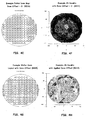
  • FIGs. 4A, 4B illustrate examples of pre-exposure metrology data;
  • FIGs. 4C, 4D illustrate a typical dose layout used to determine the gain factor for the process and the corresponding wafer CD change per unit dose, respectively;
  • FIGs. 4E, 4F illustrate a typical dose layout with dose offsets set to zero and the corresponding results of a wafer CD, respectively; and
  • FIGs. 4G, 4H illustrate a typical optimal corrected dose layout and the corresponding results of a wafer CD, respectively.
  • In the figures, corresponding reference symbols indicate corresponding parts.
  • As noted above, processes that treat the substrate wafers contribute to variations in CDU that negatively affect the quality and performance of the exposed patterns. Such non-uniformities may occur across a target field, across a wafer, and between wafers. Moreover, these non-uniformities can also vary depending a variety of factors, such as the particular path the substrate wafer travels, scheduling anomalies, etc. As described in greater detail below, the present invention contemplates a lithographic system that employs an adaptive CD enhancement process whereby these variations and non-uniformities are factored out to provide acceptable CDU levels. Such a process exploits information regarding the lithographic system, for example, wafer track processing data, metrology data, and/or substrate wafer history data, to iteratively arrive at and maintain the optimal corrective dose offsets that improve overall CDU performance.
  • FIG. 1A schematically depicts lithographic system 100 according to a particular embodiment of the invention. System 100 comprises lithographic exposure apparatus 102, which is configured to expose a pattern onto a substrate wafer, and wafer track apparatus 104, which is configured to transport the substrate wafers between the various pre- and post-exposure processing modules.
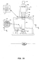
  • FIG. 1B provides a more detailed illustration of lithographic apparatus 102. As indicated in FIG. 1B, lithographic apparatus 102 includes radiation source LA and radiation system IL for providing a projection beam PB, a first object table (e.g. mask table) MT provided with a mask holder for holding a mask MA (e.g. a reticle), and a projection system PL (e.g., lens) for imaging an irradiated portion of the mask MA onto a target portion C (e.g. comprising one or more dies) of the substrate W. As depicted, lithographic apparatus 102 is of a transmissive type (i.e. has a transmissive mask). However, in general, it may also be of a reflective type, for example (with a reflective mask) and, alternatively, apparatus 102 may employ another kind of patterning devices, such as a programmable mirror array of a type as indicated above.
  • Lithographic apparatus 102 further comprises a second object table (e.g., substrate table) WT provided with a substrate holder for holding a substrate W (e.g. a resist-coated silicon wafer).
  • Source LA produces a beam of radiation, which is fed into illumination system (e.g., illuminator) IL, either directly or after having traversed conditioning mechanisms , such as a beam expander EX , for example. Illuminator IL may comprise adjusting mechanism AM for setting the outer and/or inner radial extent (commonly referred to as σ-outer and σ-inner, respectively) of the intensity distribution in the beam. In addition, it will generally comprise various other components, such as an integrator IN and a condenser CO. In this way, the beam PB impinging on the mask MA has a desired cross-sectional uniformity and intensity distribution.
  • It is to be noted with regard to FIG. 1B, that source LA may be within the housing of lithographic exposure apparatus 102 (as is often the case when the source LA is a mercury lamp, for example). However, it may also be remote from apparatus 102, as in the case of an excimer laser source. In this scenario, the remote radiation beam is guided into apparatus 102 by virtue of suitable directing mirrors. The current invention and claims encompass both of these scenarios
  • The beam PB subsequently intercepts the mask MA, which is held on a mask table MT. Having traversed the mask MA, the beam PB passes through the lens PL, which focuses the beam PB onto a target portion C of the substrate W. With the aid of the second positioning mechanism (and interferometric measuring mechanism IF), the substrate table WT can be moved accurately (e.g. so as to position different target portions C in the path of the beam PB). Similarly, the first positioning mechanism can be used to accurately position the mask MA with respect to the path of the beam PB (e.g. after mechanical retrieval of the mask MA from a mask library, or during a scan).
  • In general, movement of the object tables MT, WT will be realized with the aid of a long-stroke module (course positioning) and a short-stroke module (fine positioning), which are not explicitly depicted in FIG 1. However, in the case of a wafer stepper (as opposed to a step-and-scan apparatus), the mask table MT may just be connected to a short stroke actuator, or may be fixed.
  • Lithographic apparatus 102 can be used in two different modes:
  • (a) step mode: mask table MT is kept essentially stationary, and an entire mask image is projected in one go (i.e. a single "flash") onto a target portion C. The substrate table WT is then shifted in the x and/or y directions so that a different target portion C can be irradiated by the beam PB; and
  • (b) scan mode: essentially the same scenario applies, except that a given target portion C is not exposed in a single "flash". Instead, mask table MT is movable in a given direction (the so-called "scan direction", e.g. the y direction) with a speed v, so that projection beam PB is caused to scan over a mask image. Concurrently, substrate table WT is simultaneously moved in the same or opposite direction at a speed V = Mv, in which M is the magnification of the lens PL (typically, M = 1/4 or 1/5). In this manner, a relatively large target portion C can be exposed, without having to comon resolution.
  • FIG. 2 schematically depicts the general inventive concept of adaptive CD enhancement process 200, constructed and operative in accordance with a particular embodiment of the present invention. As indicated in FIG. 2, enhancement process 200 commences with procedure task P202 which, via lithographic exposure apparatus 102, exposes a substrate wafer W based on associated initial exposure information. This associated initial information may include pre-exposure wafer measurement data, initial exposure dosing requirements, wafer track processing data that may include the pre-specified path wafer W will travel, and metrology data see figure 4 for an example.
  • After exposing the wafer W in accordance with the initial exposure information, attributes of the exposed wafer W are measured in procedure task P204. Measurement task P204 may be configured to measure and assess a serie of wafer attributes and artifacts that relate to CD uniformity, such as the average feature size of the entire substrate, the size of the individual target fields, the thickness of the resist, thickness of the anti-reflective coating, the gap between features, X and/or Y diameter of holes and/or posts, ellipticity of holes and/or posts, area of feature, width at the top of a feature, width at the middle of a feature, width at the bottom of a feature, feature sidewall angle, line edge roughness, etc. (See, FIG. 4 for examples). These measurement may be performed by scanning electron microscope (SEM), spectroscopic ellipsometer, reflectometer, electric line width measurement (ELM), focused ion beam (FIB), e-Beam, atomic force microscope (AFM), scatterometer, defect inspection tool, overlay measurement tool, etc.
  • Based on the measured attributes of the exposed wafer W in procedure task P206, process 200 determines whether the wafer is sufficiently uniform. The sufficiency of CDU may be based on a plurality of metrics or pre-specified profile characteristics, such as, for example, CD range, CD standard deviation, average CD range between fields. If the wafer W is sufficiently uniform, as specified by the relevant metrics, procedure task P212 which archives and updates the archived correction map library 320 to indicate that no changes are required in the exposure dose offsets and the subsequent wafers will be processed with the existing exposure information.
  • If, on the other hand, wafer W is not sufficiently uniform, process 200 progresses to procedure task P208, where it adaptively compensates for the lack of CDU by generating a map of corrective exposure dose offsets. This correction map regulates the exposure levels employed by lithographic exposure apparatus 102 to correct for the variations in the wafer W CDU. As indicated in FIG. 2, this correction map is archived or stored in a correction map library 320 in order to facilitate the enhanced processing of subsequent wafers.
  • In procedure task 210, a subsequent wafer W is exposed with the latest corrective exposure dose offsets stored in correction map library 320 that correlates to the wafer history. After exposure, process 200 returns to procedure task P204 to measure the attributes of the subsequent wafer W (e.g., CD), that was exposed with the corrective dose offsets established for the specific wafer history. Process 200 then iterates to procedure task P206 to determine whether the attributes of wafer W are sufficiently uniform and, if not, an updated map of corrective exposure dose offsets are generated for each specific wafer, history condition with control limits to minimize over or under correction. Process 200 continues this iterative process until a subsequent exposed wafer W achieves the desired CDU profile. With each iteration, correction map library 320 is revised with the latest, updated corrective exposure dose offsets so that once the desired CDU profile is achieved, all subsequent wafers will be exposed with the same updated correction map. Process 200 will continue to monitor the CDU and update corrections as necessary based on the measured results.
  • By adaptively adjusting the corrective exposure dose offsets, process 200 effectively converges on the optimal corrective dose offsets to factor out wafer W variations and non-uniformities, resulting in improved CDU levels. In addition process 200 continues to monitor the CDU levels for changes over time and will calculate and implement dose adjustments as required.
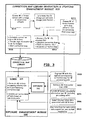
  • FIG. 3 provides a schematic functional block diagram detailing certain features and aspects of the invention described above. As depicted in FIG. 3, the adaptive CD enhancement process utilizes an exposure enhancement module 330, a correction map library enhancement module 310, and the aforementioned correction map library 320. These modules cooperate with each other in an adaptive manner to achieve the optimal corrective dose offsets.
  • Exposure enhancement module 330 relates to features and aspects of the exposure functionality and includes logical mechanism 335 which, as described in greater detail below, is configured to provide monitoring, verification, and correlation functionality. Correction map library enhancement module 310 relates to features and aspects regarding the calculation of corrective exposure dose offsets and the generation and updating of correction maps.
  • As indicated by functional block B302 of FIG. 3, a substrate wafer W is retrieved from wafer track apparatus 104, exposed by lithographic exposure apparatus 102 in accordance with associated exposure information resulting in an exposed W as indicated by functional block B308. The exposure information is supplied to, and processed by, logic mechanism 335. As discussed above and indicated by functional blocks B304 - B306, such information may include wafer track processing data containing the wafer history, modules and apparatus the wafer has been processed with, modules and apparatus the wafer will be processed with after exposure, film thickness, and metrology data. Exposure information may also include pre-exposure wafer measurement data, initial exposure dosing requirements, and similar lithographic data. Examples of pre-exposure metrology data are illustrated in FIGS. 4A, 4B.
  • Logic mechanism 335 correlates the wafer history, current substrate data, and exposure information with the information stored in the correction map library 320 to determine the corresponding dose correction map that will be used in the exposure apparatus 102. For the initial wafer W exposure, logic mechanism 335 applies no dose correction B316, unless input via the user interface B310, since no prior correction map is available. After the initial wafer exposure, logic mechanism 335 correlates the wafer processing history with the corresponding correction map, updates the corrective dose offsets, and monitors and verifies changes to the correction maps.
  • As indicated by functional blocks B308 and B312, after exposing the wafer W in accordance with the associated exposure information, attributes of the exposed wafer W are measured, CDU is assessed, corrective dose offsets are calculated, and these offsets are generated into a correction map.
  • As indicated by functional block B312, measured attributes include the CD of the wafer W as well as the CD of the individual target fields. As discussed above, other attributes that relate to CDU may also be measured, such as, for example, thickness of the resist, thickness of the anti-reflective coating, the gap between features, X & Y diameter of holes, CD sidewall angle, top-CD, middle-CD, bottom-CD, line edge roughness, etc. These measurement may be performed by scanning electron microscope (SEM), spectroscopic ellipsometer, reflectometer, electric line width measurement (ELM), focused ion beam (FIB), e-Beam, atomic force microscope (AFM), scatterometer, defect inspection tool, overlay measurement tool, etc.
  • Once the relevant attributes have been measured, an assessment is made to determine whether the wafer and/or individual target fields are sufficiently uniform in accordance with a pre-specified profile characteristic or metric, such as, for example, CD range, CD standard deviation, average CD range between fields. If wafer W is not sufficiently uniform, corrective exposure dose offsets are calculated to correct for the variations in the wafer W CDU. As discussed above, the corrective exposure dose offsets regulate the exposure dosage levels employed by lithographic exposure apparatus 102.
  • In calculating the corrective exposure dose offsets, preliminary calculations are performed, as indicated by functional blocks B314-B316, to determine baseline gain factors using known correction offsets. The gain factors for the process are determined by exposing a wafer W with the corrective exposure dose offsets replaced with a range of fixed dose offsets of known magnitude in functional block B314. FIG. 4C illustrates a typical dose layout and range, as indicated by functional block B314.
  • The resulting wafer W is measured and CD change per unit exposure dosage (gain factor) is calculated B315. FIG. 4D illustrates a typical CD change per unit exposure dosage, as calculated by functional block B315. The initial dose map is determined by exposing a wafer with a specific history with the corrective exposure dose offsets set to zero, as indicated by functional block B316, for the initial iteration. FIG. 4E illustrates a typical dose layout with dose offsets set to zero, as indicated by functional block B316 and FIG. 4F illustrates the results of the wafer W CD with the dose offsets set to zero.
  • Subsequently, as indicated in functional block B318, the correction map is correlated to the history of the corresponding wafer W and any change to the correction maps is monitored and confirmed. In addition, the correlated and confirmed correlation map is stored in correction map library 320.
  • As indicated in FIG. 3, the stored correction map corresponding to each wafer path is supplied to logic mechanism 335 where, as noted above, the wafer processing path is correlated with the corresponding correction map and the correction maps for each wafer W path is updated. This information is then supplied to lithographic exposure apparatus 102 for exposing subsequent wafers Ws.
  • As discussed above, the adaptive CD enhancement process iterates to progressively generate revised corrective exposure dose offset values and update the correction map library until an exposed wafer W is assessed to have the desired CDU, indicating that the optimal corrective dose offsets have been achieved. FIG. 4G illustrates a typical optimal corrected dose layout, captured at functional block B308 after two iterations, measured at functional block 312 and FIG. 4H illustrates the results of the wafer W CD with optimal corrected dose layout. At that point, subsequent wafers are exposed with the same updated correction map and the processed continues to be monitored. If the CDU drifts from the desired CDU, the process will identify this situation, calculate an improved dose correction map, and apply them to the exposure to continuously maintain optimal CDU. As indicated by functional block B310, data gathered and decisions made during this process are made available to the user electronically and/or visually to allow manually or automatic monitoring of the system. In addition functional block B310 allows the user to input information, and optimize the application of this invention.
  • In this manner, the adaptive process converges to the optimal corrective dose offsets, monitors the process, and corrects for changes in the process over time. In doing so, the wafer W variations and non-uniformities occurring across a target field, across a wafer, and between wafers are effectively corrected to yield the desired CDU profile.
  • The following detailed description refers to the accompanying drawings that illustrate exemplary embodiments consistent with the present invention. Other embodiments are possible and modifications may be made to the embodiments without departing from the spirit and scope of the invention. For example, the embodiments described below may, instead, be implemented in different embodiments of software, firmware, and hardware in the entities illustrated in the figures. As such, the operation and behavior of the present invention will be described with the understanding that modifications and variations of the embodiments are possible, given the level of detail present herein. Thus, the following detailed description is not meant or intended to limit the invention - rather the scope of the invention is defined by the appended claims.

Claims (21)

  1. A method of improving uniformity of substrates processed by a lithographic system having exposure apparatus to expose substrates, pre-exposure apparatus to process substrates prior to exposure, and post-exposure apparatus to process substrates after exposure, said method comprising:
    measuring attributes of substrates processed by said lithographic system;
    assessing whether said measured substrate attributes are uniform based on pre-specified substrate profile information;
    calculating corrective exposure data based on said measured substrate attributes upon determining that said measured substrate attributes are not uniform, said corrective exposure data configured to correct non-uniformities of said substrate attributes by regulating exposure dosage in said exposure apparatus of said lithographic system; and
    exposing substrates in accordance with said corrective exposure data.
  2. The method of Claim 1, further including storing collections of said corrective exposure data as correction maps.
  3. The method of Claim 1 or 2, wherein said calculation of corrective exposure data includes,
       acquiring processing module information based on information of specific apparatus of said pre-exposure apparatus and post-exposure apparatus used in processing said substrates,
       acquiring metrology information including information associated with said specific apparatus of said pre-exposure apparatus and post-exposure apparatus used in processing said substrates,
       determining exposure dosage gain factor,
       acquiring history of previously-processed substrates,
       correlating each of said correction maps to at least one of said processing module information, said metrology information, said substrate history, said exposure dosage gain factor, and said measured substrate attributes,
       iteratively calculating and updating said corrective exposure data based on at least one of said processing module information, said metrology information, said substrate history, said exposure dosage gain factor, and said measured substrate attributes,
       wherein said iterative corrective exposure data calculation and updating continues until said substrate attributes are determined to be uniform.
  4. The method of Claim 3, further including,
       monitoring and verifying said correction map correlations by a logic mechanism, and
       communicating, by said logic mechanism, with at least one of said correction maps, said processing module information, said metrology information, said substrate history, said exposure dosage gain factor, and said measured substrate attributes.
  5. The method of Claim 4, further including,
       monitoring, by said logic mechanism, said substrate attributes upon determining that said substrate attributes are uniform, and
       initiating, by said logic mechanism, invocation of corrective exposure data calculation and updating upon determining that said substrate attributes are no longer uniform.
  6. The method of Claim 5, wherein said iterative corrective exposure data calculation and updating, said monitoring of said substrate attributes, and said initiating invocation of corrective exposure data calculation and updating are controlled by said logical mechanism.
  7. The method of Claim 3, 4, 5 or 6, wherein said processing module information further includes data associated with processing path of said substrates processed by said specific apparatus of said pre-exposure apparatus and post-exposure apparatus.
  8. The method of Claim 3, 4, 5, 6 or 7, wherein said determining exposure dose gain factor includes determining change in said measured attributes of said substrates per unit of exposure dosage.
  9. The method of any one of claims 4 to 8, further including providing a user interface to communicate information regarding at least one of said exposure apparatus, said pre-exposure apparatus, said post-exposure apparatus, said correction maps, said processing module information, said metrology information, said substrate history, said exposure dosage gain factor, said measured substrate attributes, and said logical mechanism.
  10. The method of any one of claims 2 to 9, further including,
       acquiring processing module information based on information of specific apparatus of said pre-exposure apparatus and post-exposure apparatus and processing paths used in processing said substrates,
       acquiring metrology information including information associated with said specific apparatus of said pre-exposure apparatus and post-exposure apparatus used in processing said substrates,
       determining exposure dosage gain factor including calculating change in said measured attributes of said substrates per unit of exposure dosage,
       acquiring history of previously-processed substrates,
       correlating each of said correction maps to at least one of said processing module information, said metrology information, said substrate history, said exposure dosage gain factor, and said measured substrate attributes,
       iteratively calculating and updating said corrective exposure data based on at least one of said processing module information, said metrology information, said substrate history, said exposure dosage gain factor, and said measured substrate attributes, and
       providing a logical mechanism,
       wherein said logical mechanism monitors, controls, and enables said iterative corrective exposure data calculation and updating to continue until said substrate attributes are determined to be uniform upon determining that said substrate attributes are uniform, and
       wherein said logical mechanism initiates invocation of corrective exposure data calculation and updating upon determining that said substrate attributes are no longer uniform.
  11. A lithographic system that improves uniformity of substrates, comprising:
    exposure apparatus configured to expose substrates;
    pre-exposure apparatus configured to process substrates prior to exposure;
    track apparatus operatively coupled to said exposure apparatus and a plurality of processing modules;
    post-exposure apparatus configured to process substrates after exposure;
    a measuring device configured to measure attributes of said substrates; and
    a corrective exposure module that calculates corrective exposure data based on said measured attributes upon determining that said substrates are not uniform,
       wherein said corrective exposure data are configured to correct non-uniformities in said substrates by regulating exposure dosage in said exposure apparatus, and
       wherein said substrates are exposed by said exposure apparatus in accordance with said corrective exposure data.
  12. The system of Claim 11, wherein collections of said corrective exposure data are stored as correction maps in a correction map library.
  13. The system of Claim 12, wherein said calculation of corrective exposure data of said corrective exposure module includes,
       acquiring processing module information based on information of specific apparatus of said pre-exposure apparatus and post-exposure apparatus used in processing said substrates,
       acquiring metrology information including information associated with said specific apparatus of said pre-exposure apparatus and post-exposure apparatus used in processing said substrates,
       determining exposure dosage gain factor,
       acquiring history of previously-processed substrates,
       correlating each of said correction maps to at least one of said processing module information, said metrology information, said substrate history, said exposure dosage gain factor, and said measured substrate attributes,
       iteratively calculating and updating said corrective exposure data based on at least one of said processing module information, said metrology information, said substrate history, said exposure dosage gain factor, and said measured substrate attributes,
       wherein said iterative corrective exposure data calculation and updating continues until said substrate attributes are determined to be uniform.
  14. The system of Claim 12 or 13, further including a logical mechanism to monitor and verify said correction map correlations, said logical mechanism configured to communicate with at least one of said correction maps, said processing module information, said metrology information, said substrate history, said exposure dosage gain factor, and said measured substrate attributes.
  15. The system of Claim 14, wherein said logic mechanism monitors said substrate attributes upon determining that said substrate attributes are uniform, and initiates invocation of corrective exposure data calculation and updating upon determining that said substrate attributes are no longer uniform.
  16. The system of Claim 15, wherein said iterative corrective exposure data calculation and updating, said monitoring of said substrate attributes, and said initiating invocation of corrective exposure data calculation and updating are controlled by said logical mechanism.
  17. The system of Claim 13, 14, 15 and 16 wherein said processing module information further includes data associated with processing path of said substrates processed by said specific apparatus of said pre-exposure apparatus and post-exposure apparatus.
  18. The system of Claim 13, 14, 15, 16 or 17, wherein said determining exposure dose gain factor includes determining change in said measured attributes of said substrates per unit of exposure dosage.
  19. The system of any one of claims 12 to 18, further including a user interface to communicate information regarding at least one of said exposure apparatus, said pre-exposure apparatus, said post-exposure apparatus, said correction maps, said processing module information, said metrology information, said substrate history, said exposure dosage gain factor, said measured substrate attributes, and said logical mechanism.
  20. The system of any one of claims 12 to 19, wherein said adaptive calculation of corrective exposure data of said corrective exposure module includes,
       acquiring processing module information based on information of specific apparatus of said pre-exposure apparatus and post-exposure apparatus and processing paths used in processing said substrates,
       acquiring metrology information including information associated with said specific apparatus of said pre-exposure apparatus and post-exposure apparatus used in processing said substrates,
       determining exposure dosage gain factor including calculating change in said measured attributes of said substrates per unit of exposure dosage,
       acquiring history of previously-processed substrates,
       correlating each of said correction maps to at least one of said processing module information, said metrology information, said substrate history, said exposure dosage gain factor, and said measured substrate attributes,
       iteratively calculating and updating said corrective exposure data based on at least one of said processing module information, said metrology information, said substrate history, said exposure dosage gain factor, and said measured substrate attributes, and
       providing a logical mechanism,
       wherein said logical mechanism monitors, controls, and enables said iterative corrective exposure data calculation and updating to continue until said substrate attributes are determined to be uniform upon determining that said substrate attributes are uniform, and
       wherein said logical mechanism initiates invocation of corrective exposure data calculation and updating upon determining that said substrate attributes are no longer uniform.
  21. A computer program storage device comprising instructions that, when executed by a computer system, instruct the computer system to perform a process of improving uniformity of substrates according to any one of Claims 1 to 10.
EP04255674A 2003-09-17 2004-09-17 Critical dimension optimisation in lithography Withdrawn EP1517189A3 (en)

Applications Claiming Priority (2)

Application Number Priority Date Filing Date Title
US663904 2003-09-17
US10/663,904 US6873938B1 (en) 2003-09-17 2003-09-17 Adaptive lithographic critical dimension enhancement

Publications (2)

Publication Number Publication Date
EP1517189A2 true EP1517189A2 (en) 2005-03-23
EP1517189A3 EP1517189A3 (en) 2006-02-15

Family

ID=34194736

Family Applications (1)

Application Number Title Priority Date Filing Date
EP04255674A Withdrawn EP1517189A3 (en) 2003-09-17 2004-09-17 Critical dimension optimisation in lithography

Country Status (7)

Country Link
US (1) US6873938B1 (en)
EP (1) EP1517189A3 (en)
JP (1) JP4262175B2 (en)
KR (1) KR100639801B1 (en)
CN (1) CN100468201C (en)
SG (1) SG110201A1 (en)
TW (1) TWI245976B (en)

Cited By (3)

* Cited by examiner, † Cited by third party
Publication number Priority date Publication date Assignee Title
US7571021B2 (en) * 2007-02-13 2009-08-04 Taiwan Semiconductor Manufacturing Company Method and system for improving critical dimension uniformity
EP3550363A4 (en) * 2016-11-29 2019-11-06 Shanghai Micro Electronics Equipment (Group) Co., Ltd. System and method for controlling exposure dose of light source
EP4155822A1 (en) * 2021-09-28 2023-03-29 ASML Netherlands B.V. Metrology method and system and lithographic system

Families Citing this family (45)

* Cited by examiner, † Cited by third party
Publication number Priority date Publication date Assignee Title
IL148485A (en) * 2002-03-04 2008-07-08 Nova Measuring Instr Ltd Optical measurement of patterned structure parameters
US7234128B2 (en) * 2003-10-03 2007-06-19 Taiwan Semiconductor Manufacturing Company, Ltd. Method for improving the critical dimension uniformity of patterned features on wafers
US7198873B2 (en) * 2003-11-18 2007-04-03 Asml Netherlands B.V. Lithographic processing optimization based on hypersampled correlations
JP5008280B2 (en) * 2004-11-10 2012-08-22 株式会社Sokudo Substrate processing apparatus and substrate processing method
JP5154008B2 (en) * 2004-11-10 2013-02-27 株式会社Sokudo Substrate processing apparatus and substrate processing method
JP4794232B2 (en) * 2004-12-06 2011-10-19 株式会社Sokudo Substrate processing equipment
JP4926433B2 (en) * 2004-12-06 2012-05-09 株式会社Sokudo Substrate processing apparatus and substrate processing method
JP5154007B2 (en) * 2004-12-06 2013-02-27 株式会社Sokudo Substrate processing equipment
US7738075B2 (en) * 2005-05-23 2010-06-15 Asml Netherlands B.V. Lithographic attribute enhancement
JP5147167B2 (en) * 2005-07-29 2013-02-20 キヤノン株式会社 Determination method and program
KR100641505B1 (en) 2005-09-05 2006-11-01 동부일렉트로닉스 주식회사 Method for improving uniformity in a photoresist pattern critical dimension
JP4761907B2 (en) * 2005-09-28 2011-08-31 株式会社Sokudo Substrate processing equipment
JP4898419B2 (en) * 2006-01-05 2012-03-14 キヤノン株式会社 Method for determining exposure amount and focus position offset amount, program and device manufacturing method
JP2007184378A (en) * 2006-01-05 2007-07-19 Canon Inc Method and device for obtaining position of substrate for luminous exposure and/or focusing in exposure system
US7511799B2 (en) * 2006-01-27 2009-03-31 Asml Netherlands B.V. Lithographic projection apparatus and a device manufacturing method
US8294907B2 (en) * 2006-10-13 2012-10-23 Asml Netherlands B.V. Inspection method and apparatus, lithographic apparatus, lithographic processing cell and device manufacturing method
US7829249B2 (en) 2007-03-05 2010-11-09 Asml Netherlands B.V. Device manufacturing method, computer program and lithographic apparatus
US7957826B2 (en) * 2007-08-21 2011-06-07 International Business Machines Corporation Methods for normalizing error in photolithographic processes
US7871745B2 (en) * 2007-12-27 2011-01-18 United Microelectronics Corp. Exposure method
TWI380349B (en) * 2008-07-09 2012-12-21 Nanya Technology Corp Exposure method
US20120219886A1 (en) 2011-02-28 2012-08-30 D2S, Inc. Method and system for forming patterns using charged particle beam lithography with variable pattern dosage
US9323140B2 (en) 2008-09-01 2016-04-26 D2S, Inc. Method and system for forming a pattern on a reticle using charged particle beam lithography
US9341936B2 (en) 2008-09-01 2016-05-17 D2S, Inc. Method and system for forming a pattern on a reticle using charged particle beam lithography
US8473875B2 (en) 2010-10-13 2013-06-25 D2S, Inc. Method and system for forming high accuracy patterns using charged particle beam lithography
NL2003364A (en) * 2008-09-26 2010-03-29 Asml Netherlands Bv Lithographic apparatus and method.
NL2004770A (en) * 2009-05-29 2010-11-30 Asml Holding Nv LITHOGRAPHIC APPARATUS AND METHOD FOR ILLUMINATION UNIFORMITY CORRECTION AND UNIFORMITY DRIFT COMPENSATION.
JP2011081317A (en) * 2009-10-09 2011-04-21 San Ei Giken Inc Exposure device and method
US8219938B2 (en) * 2009-10-16 2012-07-10 Samsung Electronics Co., Ltd. Semiconductor inter-field dose correction
JP5165731B2 (en) * 2010-06-30 2013-03-21 東京エレクトロン株式会社 Local exposure apparatus and local exposure method
US8703389B2 (en) 2011-06-25 2014-04-22 D2S, Inc. Method and system for forming patterns with charged particle beam lithography
US9612530B2 (en) 2011-02-28 2017-04-04 D2S, Inc. Method and system for design of enhanced edge slope patterns for charged particle beam lithography
US9034542B2 (en) 2011-06-25 2015-05-19 D2S, Inc. Method and system for forming patterns with charged particle beam lithography
US8719739B2 (en) 2011-09-19 2014-05-06 D2S, Inc. Method and system for forming patterns using charged particle beam lithography
TWI562319B (en) * 2011-12-07 2016-12-11 United Microelectronics Corp Monitoring testkey used in semiconductor fabrication
US9177370B2 (en) * 2012-03-12 2015-11-03 Kla-Tencor Corporation Systems and methods of advanced site-based nanotopography for wafer surface metrology
JP5642101B2 (en) 2012-03-22 2014-12-17 株式会社東芝 Method for creating dose amount correction map, exposure method, and method for manufacturing semiconductor device
WO2013158574A1 (en) * 2012-04-18 2013-10-24 D2S, Inc. Method and system for critical dimension uniformity using charged particle beam lithography
US9343267B2 (en) 2012-04-18 2016-05-17 D2S, Inc. Method and system for dimensional uniformity using charged particle beam lithography
US8658336B2 (en) 2012-04-30 2014-02-25 Micron Technology, Inc. Methods of correcting for variation across substrates during photolithography
JP2018056143A (en) * 2014-12-26 2018-04-05 株式会社日立ハイテクノロジーズ Exposure condition evaluation system
CN106154754A (en) * 2015-04-02 2016-11-23 上海和辉光电有限公司 The control method of alignment precision and device
KR102450492B1 (en) * 2016-10-21 2022-09-30 에이에스엠엘 네델란즈 비.브이. Methods of determining corrections for a patterning process
US10503850B2 (en) * 2016-11-22 2019-12-10 Tokyo Electron Limited Generation of a map of a substrate using iterative calculations of non-measured attribute data
KR102570888B1 (en) 2017-11-23 2023-08-28 삼성전자주식회사 Method for correcting a mask layout and method of fabricating a semiconductor device using the same
US11764111B2 (en) * 2019-10-24 2023-09-19 Texas Instruments Incorporated Reducing cross-wafer variability for minimum width resistors

Citations (1)

* Cited by examiner, † Cited by third party
Publication number Priority date Publication date Assignee Title
US20020072001A1 (en) * 2000-05-04 2002-06-13 Brown Kyle A. Methods and systems for lithography process control

Family Cites Families (13)

* Cited by examiner, † Cited by third party
Publication number Priority date Publication date Assignee Title
US529872A (en) * 1894-11-27 Separator
JPS5851514A (en) * 1981-09-22 1983-03-26 Toshiba Corp Method and apparatus for exposing wafer
JPS58156938A (en) * 1982-03-12 1983-09-19 Hitachi Ltd Exposing device
US5079600A (en) * 1987-03-06 1992-01-07 Schnur Joel M High resolution patterning on solid substrates
US5523193A (en) * 1988-05-31 1996-06-04 Texas Instruments Incorporated Method and apparatus for patterning and imaging member
DE59105735D1 (en) * 1990-05-02 1995-07-20 Fraunhofer Ges Forschung EXPOSURE DEVICE.
US5229872A (en) 1992-01-21 1993-07-20 Hughes Aircraft Company Exposure device including an electrically aligned electronic mask for micropatterning
WO1997033205A1 (en) * 1996-03-06 1997-09-12 Philips Electronics N.V. Differential interferometer system and lithographic step-and-scan apparatus provided with such a system
EP0890136B9 (en) * 1996-12-24 2003-12-10 ASML Netherlands B.V. Two-dimensionally balanced positioning device with two object holders, and lithographic device provided with such a positioning device
EP1205806A1 (en) * 2000-11-09 2002-05-15 Semiconductor300 GmbH &amp; Co KG Method for exposing a semiconductor wafer
JP2002198289A (en) * 2000-12-26 2002-07-12 Hitachi Ltd Manufacturing method of semiconductor integrated circuit device
US6576385B2 (en) * 2001-02-02 2003-06-10 Advanced Micro Devices, Inc. Method of varying stepper exposure dose to compensate for across-wafer variations in photoresist thickness
EP1253497B1 (en) * 2001-04-27 2008-04-02 Qimonda Dresden GmbH & Co. oHG Method for adjusting processing parameters of plate-like objects in a processing tool

Patent Citations (1)

* Cited by examiner, † Cited by third party
Publication number Priority date Publication date Assignee Title
US20020072001A1 (en) * 2000-05-04 2002-06-13 Brown Kyle A. Methods and systems for lithography process control

Non-Patent Citations (1)

* Cited by examiner, † Cited by third party
Title
KOIKE T: "Fundamentals Of Wafer Fab Automation The Forth Generation CIM FA", 19940621; 19940621 - 19940622, 21 June 1994 (1994-06-21), pages 23 - 26, XP010300979 *

Cited By (5)

* Cited by examiner, † Cited by third party
Publication number Priority date Publication date Assignee Title
US7571021B2 (en) * 2007-02-13 2009-08-04 Taiwan Semiconductor Manufacturing Company Method and system for improving critical dimension uniformity
EP3550363A4 (en) * 2016-11-29 2019-11-06 Shanghai Micro Electronics Equipment (Group) Co., Ltd. System and method for controlling exposure dose of light source
US10642163B2 (en) 2016-11-29 2020-05-05 Shanghai Micro Electronics Equipment (Group) Co., Ltd. System and method for controlling exposure dose of light source
EP4155822A1 (en) * 2021-09-28 2023-03-29 ASML Netherlands B.V. Metrology method and system and lithographic system
WO2023051982A1 (en) * 2021-09-28 2023-04-06 Asml Netherlands B.V. Metrology method and system and lithographic system

Also Published As

Publication number Publication date
JP4262175B2 (en) 2009-05-13
KR20050028800A (en) 2005-03-23
TWI245976B (en) 2005-12-21
CN100468201C (en) 2009-03-11
EP1517189A3 (en) 2006-02-15
US20050075819A1 (en) 2005-04-07
TW200513807A (en) 2005-04-16
KR100639801B1 (en) 2006-10-30
JP2005094015A (en) 2005-04-07
US6873938B1 (en) 2005-03-29
SG110201A1 (en) 2005-04-28
CN1629729A (en) 2005-06-22

Similar Documents

Publication Publication Date Title
US6873938B1 (en) Adaptive lithographic critical dimension enhancement
US20220147665A1 (en) Process window optimizer
US8120748B2 (en) Lithographic processing optimization based on hypersampled correlations
US7580113B2 (en) Method of reducing a wave front aberration, and computer program product
JP4926115B2 (en) Method for characterizing processing steps, method for manufacturing a device, and computer program
KR100961686B1 (en) A method of performing model-based scanner tuning
TWI797362B (en) Method for determining an etch profile of a layer of a wafer for a simulation system
US7738075B2 (en) Lithographic attribute enhancement
US9791787B2 (en) Lithographic method and apparatus
IL280730B1 (en) Metrology data correction using image quality metric
US10078272B2 (en) Lithographic method and apparatus
US7177010B2 (en) Lithographic apparatus and device manufacturing method
US7856606B2 (en) Apparatus, method and program product for suppressing waviness of features to be printed using photolithographic systems
US20050030507A1 (en) Lithographic apparatus, device manufacturing method, and device manufactured thereby
JP2004235460A (en) Exposure system, scanning exposure apparatus and exposure method
US20240142959A1 (en) Method for decoupling sources of variation related to semiconductor manufacturing

Legal Events

Date Code Title Description
PUAI Public reference made under article 153(3) epc to a published international application that has entered the european phase

Free format text: ORIGINAL CODE: 0009012

AK Designated contracting states

Kind code of ref document: A2

Designated state(s): AT BE BG CH CY CZ DE DK EE ES FI FR GB GR HU IE IT LI LU MC NL PL PT RO SE SI SK TR

AX Request for extension of the european patent

Extension state: AL HR LT LV MK

PUAL Search report despatched

Free format text: ORIGINAL CODE: 0009013

AK Designated contracting states

Kind code of ref document: A3

Designated state(s): AT BE BG CH CY CZ DE DK EE ES FI FR GB GR HU IE IT LI LU MC NL PL PT RO SE SI SK TR

AX Request for extension of the european patent

Extension state: AL HR LT LV MK

17P Request for examination filed

Effective date: 20060322

AKX Designation fees paid

Designated state(s): DE FR GB IT NL

17Q First examination report despatched

Effective date: 20070214

STAA Information on the status of an ep patent application or granted ep patent

Free format text: STATUS: THE APPLICATION IS DEEMED TO BE WITHDRAWN

18D Application deemed to be withdrawn

Effective date: 20101230