EP1515436A2 - Surface acoustic wave element and electronic equipment provided with the element - Google Patents
Surface acoustic wave element and electronic equipment provided with the element Download PDFInfo
- Publication number
- EP1515436A2 EP1515436A2 EP04019789A EP04019789A EP1515436A2 EP 1515436 A2 EP1515436 A2 EP 1515436A2 EP 04019789 A EP04019789 A EP 04019789A EP 04019789 A EP04019789 A EP 04019789A EP 1515436 A2 EP1515436 A2 EP 1515436A2
- Authority
- EP
- European Patent Office
- Prior art keywords
- surface acoustic
- acoustic wave
- wave element
- reflector
- piezoelectric layer
- Prior art date
- Legal status (The legal status is an assumption and is not a legal conclusion. Google has not performed a legal analysis and makes no representation as to the accuracy of the status listed.)
- Withdrawn
Links
Images





Classifications
-
- H—ELECTRICITY
- H03—ELECTRONIC CIRCUITRY
- H03H—IMPEDANCE NETWORKS, e.g. RESONANT CIRCUITS; RESONATORS
- H03H9/00—Networks comprising electromechanical or electro-acoustic elements; Electromechanical resonators
- H03H9/25—Constructional features of resonators using surface acoustic waves
-
- H—ELECTRICITY
- H03—ELECTRONIC CIRCUITRY
- H03H—IMPEDANCE NETWORKS, e.g. RESONANT CIRCUITS; RESONATORS
- H03H9/00—Networks comprising electromechanical or electro-acoustic elements; Electromechanical resonators
- H03H9/02—Details
- H03H9/02535—Details of surface acoustic wave devices
- H03H9/02543—Characteristics of substrate, e.g. cutting angles
- H03H9/02574—Characteristics of substrate, e.g. cutting angles of combined substrates, multilayered substrates, piezoelectrical layers on not-piezoelectrical substrate
Definitions
- the present invention relates to a surface acoustic wave element and electronic equipment provided with the element.
- a wave which is propagated by concentrating its energy in the vicinity of the surface of a propagation medium is known as a Surface Acoustic Wave (SAW).
- SAW Surface Acoustic Wave
- a surface acoustic wave element is a device utilizing such a surface acoustic wave.
- the surface acoustic wave element is used in a band pass filter for communication equipment such as a mobile telephone, a resonator as a reference clock, a delay element for signal processing (inparticular, a fourier transform functional element), various kinds of sensors such as a pressure sensor and a temperature sensor, an optical deflector, and the like.
- a surface acoustic wave element used as a filter or a resonator for example, comprises a piezoelectric base body as the propagation medium of the surface acoustic wave, a pair of interdigital transducers (ITDs) arranged on the piezoelectric base body, one for input which applies a voltage to excite a surface acoustic wave in the piezoelectric base body, and another for output which detects a surface acoustic wave propagating on the piezoelectric base body and outputs the wave by converting it into an electrical signal, and a pair of reflectors arranged on both sides of the combined IDTs.
- the IDTs and the reflectors are respectively formed from a layer of conductive material such as Aluminum.
- the generated surface acoustic wave propagates on both sides of the IDT, and then it is reflected by the reflectors, which gives rise to a resonance in the space between the reflectors.
- the energy of the surface acoustic wave is converted into electrical energy by the output IDT, and it is outputted from the output IDT.
- the factors which determine the impedance characteristic of the resonator and the insertion loss in the filter include an electrode finger pitch Pt of the IDT and a reflecting body pitch Pr of the reflector.
- the electrode finger pitch Pt and the reflecting body pitch Pr are set respectively to about one half of the wavelength ⁇ of the surface acoustic wave.
- the thickness of the IDT and the reflector is small or the specific gravity of the constituent materials of these components is relatively low, it is possible to match the frequency of the surface acoustic wave of the IDT and the frequency of the surface acoustic wave of the reflectors by setting the electrode finger pitch Pt to be equal to the reflecting body pitch Pr, thereby enabling the impedance characteristic and the insertion loss to be improved.
- the thickness of the IDT and the reflector in response to their required functions. For example, when a high reflectance of the surface acoustic waves of the IDT and by the reflector is desired, it is preferred that the thickness of the IDT and the reflector is relatively large.
- Such a phenomenon becomes particularly conspicuous when a material with relatively high specific gravity is used as the constituent material for the IDT and the reflector.
- the present invention has been made in view of the problem in the prior art described above, and therefore it is an object of the present invention to provide a surface acoustic wave element employing a substrate having a piezoelectric layer by which it is possible to improve the impedance characteristic and the insertion loss of the element, and an electronic equipment provided with the surface acoustic wave element.
- the present invention is directed to a surface acoustic wave element, which comprises a substrate; a piezoelectric layer arranged on the substrate and mainly formed of a piezoelectric material; an interdigital transducer arranged on the piezoelectric layer for converting an electrical signal into a surface acoustic wave and/or for converting a surface acoustic wave into an electrical signal, and the interdigital transducer including a plurality of electrode fingers juxtaposed with a prescribed spacing; and a reflector arranged adjacent to the interdigital transducer on the piezoelectric layer, the first reflector including a plurality of reflecting bodies juxtaposed with a prescribed spacing, wherein a pitch of the reflecting body of the reflector is made to be smaller than a pitch of the electrode finger of the interdigital transducer.
- the surface acoustic wave element having the above structure it is possible to improve the impedance characteristic and the insertion loss of the acoustic wave element employing the substrate having the piezoelectric layer.
- the pitch of the electrode finger of the interdigital transducer and the pitch of the reflecting body of the reflector are defined as Pt [ ⁇ m] and Pr [ ⁇ m], respectively, the ratio Pr/Pt is in the range of 0.7 to 0.9995. This makes it possible to improve the impedance characteristic and the insertion loss of the element more reliably.
- a thickness of the piezoelectric layer is equal to or less than twice a wavelength of the surface acoustic wave to be excited in the piezoelectric layer.
- the present invention is especially preferably applied to the surface acoustic wave element having such a thickness.
- the surface acoustic wave element further comprises an intermediate layer which is provided between the piezoelectric layer and the substrate for setting the characteristics of the surface acoustic waves excited in the piezoelectric layer. This makes it possible to set the characteristic of the surface acoustic wave to a desired characteristic.
- the intermediate layer is formed of a material which contains as a major component thereof at least one material selected from the group comprising diamond, sapphire, alumina, silicon, silicon nitride, glass, crystalline quartz, lithium tantalate and potassium niobate. Formation of the intermediate layer from such a material makes it possible to contribute to realizing surface acoustic waves of high frequencies that are required in the high-speed communications fields such radio frequency LANs or optical communications.
- the piezoelectric layer is formed of a material which contains as a major component thereof at least one material selected from the group comprising zinc oxide,aluminum nitride,lithium tantalate,lithium niobate and potassium niobate. Formation of the intermediate layer from such a material makes it possible to obtain a surface acoustic wave element of high frequency type and having excellent heat resistance.
- the separation distance between the interdigital transducer and the reflector is in the range of 0.05 to 0.4 time the wavelength of the surface acoustic wave excited in the piezoelectric layer or the sum of this value and an integer multiple of the wavelength. This makes it possible for the reflector to perform resonance of surface acoustic waves efficiently.
- the surface acoustic wave element further comprises a second reflector, wherein the reflector and the second reflector are arranged on both sides of the interdigital transducer on the piezoelectric layer. This makes it possible to confine the surface acoustic waves therebetween to resonate them.
- the configuration of the second reflector is substantially the same as the configuration of the reflector. This also makes it possible to confine the surface acoustic waves therebetween to resonate them more dynamically.
- Another aspect of the present invention is directed to an electronic equipment provided with the surface acoustic wave element as described above.
- Fig. is a plan view showing a first embodiment of the surface acoustic wave element according to the present invention
- Fig. 2 is a sectional view of the surface acoustic wave element shown in Fig. 1.
- the upper and the lower sides of Fig. 2 will be referred to as “upper” and “lower,” respectively.
- a surface acoustic wave element 1 shown in each of the drawings comprises a substrate 2, an intermediate layer 3 and a piezoelectric layer 4 which are laminated on the substrate 2, an IDT 5 disposed on the piezoelectric layer 4, a pair of reflectors 6 and 7 arranged on both sides of the IDT 5, and a protective layer 8 provided so as to cover the IDT 5 and the reflectors 6 and 7.
- Examples of a constituent material for the substrate 2 include various kinds of semiconductor material such as Si, GaSi, SiGe, GaAs, STC and InP, crystalline quartz, various kinds of glass material, various kinds of ceramic material, various kinds of resin material such as polyimide and polycarbonate, and the like.
- the average thickness of the substrate 2 is not particularly limited, but it is preferably in the range of 0.05 to 1 mm, and more preferably in the range of 0.1 to 0.8 mm.
- the substrate 2 may be formed into a single layer or into a laminate of several layers. In the latter case, materials described in the above may be selectively used for each of the layers in an arbitrary combination.
- the intermediate layer 3 is provided between the piezoelectric layer 4 and the substrate 2, and has a function of setting the characteristics (regulating the conditions) of the surface acoustic waves excited in the piezoelectric layer 4.
- the characteristics the oscillation frequency, amplitude, propagation velocity, and the like can be mentioned.
- the characteristics of the surface acoustic waves may be set to desired levels.
- the constituent material of the intermediate layer 3 it is preferable to employ a material which contains as a major component thereof at least one material selected from the group comprising diamond, sapphire, alumina, silicon, silicon nitride, glass, crystalline quartz, quartz, lithium tantalite, and potassium niobate, and the like.
- a material which contains as major component thereof at least one material selected from among diamond, sapphire, lithium tantalite, and potassium niobate By constituting the intermediate layer 3 with such a material, it is possible to contribute to realizing surface acoustic waves of high frequencies that are required in the high-speed communications fields such radio frequency LANs or optical communications.
- the optimum average thickness of the intermediate layer 3 may have varying values depending upon the frequency and the desired characteristics, it is preferably in the range of 1 to 20 ⁇ m, more preferably in the range of 3 to 10 ⁇ m, and even more preferably in the range of 3 to 5 ⁇ m.
- the intermediate layer 3 may be formed into a single layer or a laminate structure formed of a plurality of layers in accordance with the characteristics of the required surface acoustic wave.
- the intermediate layer 3 is provided in accordance with a special need, so that normal operation can be done without it.
- the piezoelectric layer 4 functions as the propagation medium of the surface acoustic wave.
- the constituent material for the piezoelectric layer 4 it is preferable to use a material which contains as a major component thereof at least one material which is selected from among zinc oxide, aluminum nitride, lithium tantalate, lithium niobate, and potassium niobate.
- a material which contains as a major component thereof at least one material which is selected from among zinc oxide, aluminum nitride, lithium tantalate, lithium niobate, and potassium niobate.
- a material which contains as a major component thereof at least one material which is selected from among zinc oxide, aluminum nitride, lithium tantalate, lithium niobate, and potassium niobate By constituting the piezoelectric layer 4 using such a material, it is possible to obtain a surface acoustic wave element 1 that is of high frequency and has an excellent temperature characteristic.
- the substrate 2 is a piezoelectric substrate, it is possible to obtain a surface acoustic wave element that has a pie
- the thickness of the piezoelectric layer 4 varies somewhat depending upon the constituent material or the like of the piezoelectric layer 4 and hence is not particularly limited to a specific value, it is preferable that the thickness is less than twice the wavelength of the surface acoustic wave excited in the piezoelectric layer 4, and more preferably in the range of 0.01 to 1 time the wavelength. If the thickness of the piezoelectric layer 4 is too small, there is a possibility that a surface acoustic wave may not be excited. On the other hand, if the thickness of the piezoelectric layer 4 is too large, there is a possibility that the effect of the present invention that will be described later may not be realized.
- the IDT is of the so-called one-port type, and has electrodes 5a and 5b that possess a function of exciting a surface acoustic wave in the piezoelectric layer 4 when a voltage is applied to the piezoelectric layer 4.
- each of the electrodes 5a and 5b also has the function of converting the surface acoustic wave into an electrical signal.
- each of the reflectors 6 and 7 possesses the function of reflecting the surface acoustic wave that propagates in the piezoelectric layer 4, and conf ining it in the space between the reflectors 6 and 7.
- the electrodes 5a and 5b have respectively a plurality of electrode fingers 51 juxtaposed with a prescribed spacing, and form an interdigital structure as a whole.
- the reflectors 6 and 7 have respectively a plurality of reflecting bodies (teeth) 61 and 71, juxtaposed with a prescribed spacing, forming as a whole a comb-shaped structure, respectively. In this way, each of the reflectors 6 and 7 is configured so as to be able to reflect the surface acoustic wave with high efficiency.
- the width, spacing, pitch, thickness, and the like of the electrode fingers 51 and the reflecting bodies 61 and 71 it is possible to set the characteristics such as the oscillation frequency of the surface acoustic wave to desired values.
- the specific conditions for these quantities will be described in detail later.
- each of the reflectors 6 and 7 may be made mutually the same or different, but by giving substantially the same configuration to the both reflectors, the surface acoustic wave can be confined more reliably between the reflector 6 and the reflector 7. As a result, it is possible to make the surface acoustic wave resonate more strongly.
- Al, Cu, W, Mo, Ti, Au, Ta, Ni, Cr and Ge, and the like, or alloys including these elements may be mentioned, and one kind or two or more kinds of these materials in combination may be used.
- the protective layer 8 is provided for preventing adherence of foreign matters to the surface of the IDT 5 and the reflectors 6 and 7, and for preventing short-circuit between the electrode fingers via foreign matters.
- the constituent material for the protective layer 8 it is preferable to use a material which contains as a major component thereof at least one of silicon oxide, silicon nitride and aluminum oxide. By constituting the protective layer 8 using such a material, it is possible to form the protective layer 8 easily, and make the protective layer 8 excellent in insulation as well.
- the protective layer 8 may be formed so as to cover the entire surface of the IDT 5 and the reflectors 6 and 7 as shown in Fig. 2, but it may be formed on the upper surface of the IDT 5 and the reflectors 6 and 7 corresponding to their patterns, with the side faces of the IDT 5 and the reflectors 6 and 7 exposed to the air. With such an arrangement, energy loss generated during the propagation of the surface acoustic wave can be suppressed to a low level.
- the protective layer 8 also functions for correcting the temperature characteristic, for which an optimum value is set by finding the temperature characteristics of the piezoelectric layer and the intermediate layer.
- the average thickness of the protective layer 8 is not particularly limited, it is preferable that the thickness is in the range of 10 to 1,500 nm, and more preferably in the range of 30 to 400 nm. By restricting the thickness of the protective layer 8 to the above range, it is possible to achieve sufficient insulation and obtain satisfactory temperature characteristic while preventing or suppressing lowering of the oscillation frequency of the surface acoustic wave accompanying the increase in the mass.
- the IDT 5 (each of the electrodes 5a and 5b) has a plurality of electrode fingers 51 juxtaposed with a prescribed spacing
- the reflectors 6 and 7 have respectively a plurality of reflecting bodies (teeth) 61 and 71 juxtaposed with a prescribed spacing.
- the pitch Pr of the reflecting body of each reflector 6 and 7 is set to be smaller than the pitch Pt of the electrode finger of the IDT 5.
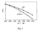
- a graph showing the dependence (relation) between the frequencies of the surface acoustic wave at the IDT and at the reflector and the film thickness of the IDT and the reflector is shown in Fig. 3.
- the abscissa represents the normalized value obtained by dividing the film thickness H of the IDT or each reflector 6 and 7 by the wavelength ⁇ of the surf ace acoustic wave
- the IDT and the reflectors 6 and 7 are formed of Al, respectively.
- both of the frequencies f/f0 of the surface acoustic waves at the IDT 5 and at respective reflectors 6 and 7 decrease as H/ ⁇ increases, with the decreasing rate for the reflectors 6 and 7 being the larger. Because of this, the difference between the frequency of the surface acoustic wave at the IDT 5 and the frequency of the surface acoustic wave at the reflectors 6 and 7 increases as H/ ⁇ gets large.
- the frequencies f of the surface acoustic waves at the IDT 5 and at the reflectors 6 and 7 become high as the electrode finger pitch Pt and the reflecting body pitch Pr decrease.
- the frequency decrease curve of the surface acoustic wave at the reflectors 6 and 7, as shown in the graph in Fig. 3, is shifted upward, and the difference between the frequency of the surface acoustic wave at the IDT 5 and the frequency of the surface acoustic wave at the reflectors 6 and 7 becomes small.
- an improvement in the impedance characteristic and the insertion loss can be achieved in the surface acoustic wave element 1.
- the improvement on the impedance characteristic and the insertion loss can be achieved by setting the relationship between the electrode finger pitch Pt and the reflecting body pitch Pr as in the above, while aiming at improvement in various characteristics of the surface acoustic wave element 1 by enhancing the reflectance through increase in the film thickness of the IDT 5 and the reflectors 6 and 7, and forming the IDT 5 and the reflectors using amaterial (for example, gold, chromium, tungsten, titanium, copper or the like) having a relatively high specific gravity.
- amaterial for example, gold, chromium, tungsten, titanium, copper or the like
- the ratio Pr/Pt is in the range of 0.7 to 0.9995, and more preferably in the range of 0.8 to 0.99.
- the average thickness of the IDT 5 and the reflectors 6 and 7 varies somewhat depending upon the functions desired of the surface acoustic wave element 1, it is preferable that it is in the range of 10 to 2,000 nm.
- the separation distance g between the IDT 5 and the respective reflectors 6 and 7 is preferably in the range of 0.05 to 0.4 time the wavelength of the surface acoustic wave excited in the piezoelectric layer 4 or the sum of this value and an integer multiple of the wavelength, and more preferably in the range of 0.2 to 0.3 time the wavelength or the sum of this value and an integer multiple of the wavelength.
- a graph showing the dependence (relation) between the frequency of the surface acoustic wave at the IDT and at the reflector and the film thickness of the IDT and the reflector is shown in Fig. 4 for a surface acoustic wave element having apiezoelectric substrate of a single layer configuration.
- the reduction rate (H/ ⁇ ) depending upon the film thickness is larger for the frequency of the surface acoustic wave at the IDT as compared with the frequency of the surface acoustic wave at the reflector, contrary to the case shown in Fig. 3.
- the reflecting body pitch is set smaller than the electrode finger pitch, the difference between the frequency of the surface acoustic wave at the IDT and the frequency of the surface acoustic wave at each reflector becomes large on the contrary, thus impairing the impedance characteristic and the insertion loss of the surface acoustic wave element.
- the improvement effect due to setting the reflecting body pitch to be smaller than the electrode finger pitch is a peculiar effect as seen in the case of the surface acoustic wave element 1 having a multilayer configuration in which at least a piezoelectric layer is formed on the substrate.
- Fig. 5 is a plan view showing the second embodiment of the surface acoustic wave element according to this invention
- Fig. 6 is a sectional view of the surface acoustic wave element shown in Fig. 5.
- the upper side and the lower side of Fig. 6 will be referred to “upper” and “lower, " respectively.
- the surface acoustic wave element 9 of the second embodiment is the same as the first embodiment except for the fact that an IDT 10 for input and an IDT 11 for output are provided in place of the IDT 5 which possesses both of the function of exciting a surface acoustic wave and the function of converting the surface acoustic wave into an electrical signal.
- the input side electrode IDT 10 has a function of exciting a surface acousticwave in the piezoelectric layer 4 when avoltage is applied to the piezoelectric layer 4, whereas the output side electrode IDT 11 has a function of detecting a surface acoustic wave propagating on the piezoelectric layer 4, and outputting the surface acoustic wave by converting it into an electrical signal.
- the IDTs 10 and 11 have respectively an interdigital structure having pluralities of electrode fingers 101 and 111 juxtaposed with prescribed spacing, and by adjusting the width, spacing, pitch, thickness or the like of the electrode fingers 101 and 111 of respective IDTs 10 and 11, it is possible to set the characteristics such as the frequencies of the surface acoustic waves to desired values.
- the reflecting body pitch Pr of respective reflectors 6 and 7 is set smaller than the electrode finger pitch Pt of respective IDTs 10 and 11. With this setting, the frequencies of the surface acoustic waves at the respective IDTs 10 and 11, and the frequencies of the surface acoustic waves at the respective reflectors 6 and 7 can be made almost equal, so that an improvement on the impedance characteristic and the insertion loss can be realized in the surface acoustic wave element 9.
- the surface acoustic wave elements 1 and 9 as described in the above can be applied to various kinds of electronic equipment to obtain electronic equipment of high reliability.
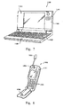
- Fig.7 is a perspective view showing the configuration of amobile (or notebook type) personal computer which is one example of electronic equipment provided with the surface acoustic wave element of this invention.
- a personal computer 1100 comprises a computer body 1104 equipped with an antenna 1101 and a keyboard 1102, and a display unit 1106, and the display unit 1106 is supported turnably by the computer body 1104 via a hinge mechanism.
- the surface acoustic wave element 1 (or 9) that functions as a filter, a resonator, a reference clock, or the like is built in.
- Fig. 8 is a perspective view showing the configuration of a mobile telephone (including a PHS) which is another example of electronic equipment provided with the surface acoustic wave element of this invention.
- a mobile telephone 1200 is provided with an antenna 1201, a plurality of operation buttons 1202, an ear piece 1204 and a mouth piece 1206, and a display part is arranged between the operation buttons 1202 and the ear piece 1204.
- the surface acoustic wave element 1 (or 9) functioning as a filter, a resonator, or the like is built in.
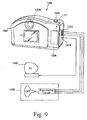
- Fig. 9 is a perspective view showing the configuration of a digital still camera which is other example of electronic equipment provided with the acoustic wave element according to this invention. In the figure, the connection with external equipment is shown in a simplified manner.
- an imaged signal (picture signal) is created by phtoelectrically converting the optical image of the object by an imaging element such as a CCD (charge coupled device).
- CCD charge coupled device
- a display part provided on the back face of a case (body) 1302 of the digital still camera 1300 performs display based on the signal imaged by the CCD, and the display part functions as a finder which displays the object as an electronic image.
- a light receiving unit 1304 which includes an optical lens (imaging optics), the CCD, and the like are provided on the front side (back side of the figure) of the case 1302.
- the imaging signal of the CCD at that moment is transferred to a memory 1308 and is stored therein.
- a video signal output terminal 1312 and an input/output terminal 1314 are provided on a side face of the case 1302.
- a television monitor 1430 and a personal computer 1440 are connected to the video signal output terminal 1312 and the input/output terminal 1314 for data communication, respectively, as needed.
- the system is configured such that imaged signals stored in the memory 1308 are output to the television monitor 1430 or the personal computer 1440 by a prescribed operation.
- the surface acoustic wave element 1 (or 9) to function as a filter or a resonator.
- an ink jet discharge device for example, ink jet printer
- laptop personal computer television receiver, video camera, video tape recorder, car navigation device, pager, electronic notebook (including one with communication function), electronic dictionary, desktop calculator, electronic game machine, word processor, work station, video telephone, crime prevention video monitor, electronic binocular, POS terminal, medical equipment (for example, electronic clinical thermometer, blood pressure gauge, blood sugar meter, electrocardiogram measurement instrument, ultrasonic diagnostic equipment and electronic endoscope), fish finder, various kinds of measurement equipment, instruments (f or example, instruments for train, aircraft and ship), flight simulator, or the like.
- ink jet discharge device for example, ink jet printer
- laptop personal computer television receiver, video camera, video tape recorder, car navigation device, pager, electronic notebook (including one with communication function), electronic dictionary, desktop calculator, electronic game machine, word processor, work station, video telephone, crime prevention video monitor, electronic binocular, POS terminal, medical equipment (for example, electronic clinical thermometer, blood pressure gauge, blood sugar meter, electrocardiogram measurement instrument, ultrasonic
- the surface acoustic wave element of the present invention may further be providedwith a temperature compensation film that has a function of improving the temperature characteristic.
- an intermediate layer of an arbitrary purpose may be provided between various layers constituting the surface acoustic wave element of the present invention.
- the surface acoustic wave element of the present invention may be compounded with semiconductor elements having various functions.
- a silicon substrate having the average thickness of 0.4 mm was prepared as the substrate.
- a diamond layer (intermediate layer) having the average thickness of 10 ⁇ m and a zinc oxide layer (piezoelectric layer) having the average thickness of 400 nm were formed on the substrate by laminating them sequentially.
- the average thickness of the zinc oxide layer was 0.1 time the wavelength of the surface acoustic wave.
- a resist film corresponding to the shapes of the IDT and the reflectors were formed on the conductive material layer.
- the IDT and the reflectors were formed by removing unnecessary portions of the conductive material layer by dry etching using the resist film as a mask.
- the separation distance g between the IDT and the respective reflectors was set to 1 ⁇ m (0.25 time the wavelength of the surface acoustic wave).
- a silicon oxide layer (protective layer) of average thickness 400 nm was formed on the zinc oxide layer by adhering silicon oxide (SiO 2 ) by CVD or PVD so as to cover the IDT and the reflectors, obtaining the surface acoustic wave element as shown in Fig.1 and Fig.2.
- the surface acoustic wave element as shown in Fig. 5 and Fig. 6 was obtained in a manner similar to the first example except for the formation of the IDT for input and the IDT for output.
- the electrode finger pitch Pt for the IDTs, the reflecting body pitch Pr for the reflectors and the separation distance g between the IDT and the reflector were set respectively to be the same as in the example 1.
- a surface acoustic wave element was obtained in a manner similar to example 1 except for the electrode finger pitch Pt of the IDT and the reflecting body pitch Pr of the reflector were set to 2 ⁇ m, respectively, and the separation distance g between the IDT and the reflector was set to 1 ⁇ m.
- a surface acoustic wave element was obtained in a manner similar to example 2 except for the electrode finger pitch Pt of the IDT and the reflecting body pitch Pr of the reflector were set to 2 ⁇ m, respectively, and the separation distance g between the IDT and the reflector wasiset 1 ⁇ m.
- the impedance characteristic was examined for the surface acoustic wave elements prepared respectively for the Example 1 and the Comparative example 1.
- Fig. 10 The result is shown in Fig. 10.
- the abscissa represents the frequency deviation with respect to the reference frequency, and the ordinate represents the impedance.
- the surface acoustic wave element of the Example 1 of this invention realizes an improvement on the impedance characteristic as compared with the surface acoustic wave device of the Comparative example 1.
- the insertion loss (energy loss) was examined for the surface acoustic wave elements prepared for the Example 2 and the Comparative example 2.
- Fig. 11 the abscissa represents the frequency of the surface acoustic wave, and the ordinate represents the insertion loss.
- the surface acoustic wave element of the Example 2 of this invention realizes an improvement on the insertion loss as compared with the surface acoustic wave device of the Comparative example 2.
- a surface acoustic wave element was prepared similar to the Example 1 and the Example 2 by forming a zinc oxide layer on the crystalline quartz substrate, and forming the IDTs and the reflectors on the zinc oxide layer to examine the impedance characteristic and the insertion loss.
Landscapes
- Physics & Mathematics (AREA)
- Acoustics & Sound (AREA)
- Surface Acoustic Wave Elements And Circuit Networks Thereof (AREA)
Abstract
Description
Claims (10)
- A surface acoustic wave element, comprising:a substrate;a piezoelectric layer arranged on the substrate and mainly formed of a piezoelectric material;an interdigital transducer arranged on the piezoelectric layer for converting an electrical signal into a surface acoustic wave and/or for converting a surface acoustic wave into an electrical signal, and the interdigital transducer including a plurality of electrode fingers juxtaposed with a prescribed spacing; anda reflector arranged adjacent to the interdigital transducer on the piezoelectric layer, the first reflector including a plurality of reflecting bodies juxtaposed with a prescribed spacing, wherein a pitch of the reflecting body of the reflector is made to be smaller than a pitch of the electrode finger of the interdigital transducer.
- The surface acoustic wave element as claimed in claim 1, wherein when the pitch of the electrode finger of the interdigital transducer and the pitch of the reflecting body of the reflector are defined as Pt [µm] and Pr [µm], respectively, the ratio Pr/Pt is in the range of 0.7 to 0.9995.
- The surface acoustic wave element as claimed in claim 1, wherein a thickness of the piezoelectric layer is equal to or less than twice a wavelength of the surface acoustic wave to be excited in the piezoelectric layer.
- The surface acoustic wave element as claimed in claim 1, further comprising an intermediate layer provided between the piezoelectric layer and the substrate for setting the characteristics of the surface acoustic waves excited in the piezoelectric layer.
- The surface acoustic wave element as claimed in claim 4, wherein the intermediate layer is formed of a material which contains as a major component thereof at least one material selected from the group comprising diamond, sapphire, alumina, silicon, silicon nitride, glass, crystalline quartz, lithium tantalate and potassium niobate.
- The surface acoustic wave element as claimed in claim 1, wherein the piezoelectric layer is formed of a material which contains as a major component thereof at least one material selected from the group comprising zinc oxide, aluminum nitride, lithium tantalate, lithium niobate and potassium niobate.
- The surface acoustic wave element as claimed in claim 1, wherein the separation distance between the interdigital transducer and the reflector is in the range of 0.05 to 0.4 time the wavelength of the surface acoustic wave excited in the piezoelectric layer or the sum of this value and an integer multiple of the wavelength.
- The surface acoustic wave element as claimed in claim 1, further comprising a second reflector, wherein the reflector and the second reflector are arranged on both sides of the interdigital transducer on the piezoelectric layer.
- The surface acoustic wave element as claimed in claim 8, wherein the configuration of the second reflector is substantially the same as the configuration of the reflector.
- An electronic equipment provided with the surface acoustic wave element claimed in any one of claims 1 to 9.
Applications Claiming Priority (2)
| Application Number | Priority Date | Filing Date | Title |
|---|---|---|---|
| JP2003307371 | 2003-08-29 | ||
| JP2003307371 | 2003-08-29 |
Publications (2)
| Publication Number | Publication Date |
|---|---|
| EP1515436A2 true EP1515436A2 (en) | 2005-03-16 |
| EP1515436A3 EP1515436A3 (en) | 2005-08-31 |
Family
ID=34131802
Family Applications (1)
| Application Number | Title | Priority Date | Filing Date |
|---|---|---|---|
| EP04019789A Withdrawn EP1515436A3 (en) | 2003-08-29 | 2004-08-20 | Surface acoustic wave element and electronic equipment provided with the element |
Country Status (5)
| Country | Link |
|---|---|
| US (1) | US7245193B2 (en) |
| EP (1) | EP1515436A3 (en) |
| KR (1) | KR100678797B1 (en) |
| CN (1) | CN1592099A (en) |
| TW (1) | TWI292252B (en) |
Cited By (3)
| Publication number | Priority date | Publication date | Assignee | Title |
|---|---|---|---|---|
| EP1708289A3 (en) * | 2005-03-29 | 2007-05-23 | Seiko Epson Corporation | Piezoelectric film laminate and method of manufacturing the same, surface acoustic wave device, frequency filter, oscillator, electronic circuit, and electronic instrument |
| RU2455753C1 (en) * | 2011-03-01 | 2012-07-10 | Юрий Сергеевич Иванченко | Oscillator with laser excitation of quartz resonator |
| WO2018046561A1 (en) * | 2016-09-07 | 2018-03-15 | Robert Bosch Gmbh | Tunable lithium niobate resonators and filters via lithiation and delithiation |
Families Citing this family (84)
| Publication number | Priority date | Publication date | Assignee | Title |
|---|---|---|---|---|
| US8470019B1 (en) * | 2001-11-30 | 2013-06-25 | Advanced Cardiovascular Systems, Inc. | TiNxOy modified surface for an implantable device and a method of producing the same |
| US7760048B2 (en) * | 2004-04-19 | 2010-07-20 | Murata Manufacturing Co., Ltd. | Elastic wave filter and communication device equipped with the elastic wave filter |
| JP2007202087A (en) * | 2005-05-11 | 2007-08-09 | Seiko Epson Corp | Lamb wave type high frequency device |
| JP4412292B2 (en) * | 2006-02-06 | 2010-02-10 | セイコーエプソン株式会社 | Surface acoustic wave device and electronic apparatus |
| JP2008078739A (en) * | 2006-09-19 | 2008-04-03 | Fujitsu Media Device Kk | Elastic wave device and filter |
| JP5129004B2 (en) * | 2008-04-16 | 2013-01-23 | オリンパス株式会社 | Endoscope device |
| JP2010068503A (en) * | 2008-08-13 | 2010-03-25 | Seiko Epson Corp | Surface acoustic wave element |
| JP4835700B2 (en) * | 2009-01-26 | 2011-12-14 | 株式会社デンソー | Surface acoustic wave pressure sensor |
| JP5330180B2 (en) * | 2009-10-02 | 2013-10-30 | オリンパス株式会社 | Endoscope device |
| CN102567779A (en) * | 2012-01-05 | 2012-07-11 | 天津理工大学 | Surface acoustic wave radio frequency identification tag of interdigital transducer / zinc oxide / aluminum (IDT / ZnO / AL) / diamond multilayer membrane structure |
| US10333487B2 (en) * | 2014-07-30 | 2019-06-25 | Kyocera Corporation | Acoustic wave element, filter element, and communication device |
| CN104359584A (en) * | 2014-11-12 | 2015-02-18 | 中国科学院微电子研究所 | High-temperature surface acoustic wave temperature sensor |
| KR101923572B1 (en) * | 2015-03-16 | 2018-11-29 | 가부시키가이샤 무라타 세이사쿠쇼 | Seismic wave device and manufacturing method thereof |
| CN107615657B (en) * | 2015-06-25 | 2020-12-01 | 株式会社村田制作所 | elastic wave device |
| KR102250789B1 (en) * | 2015-09-07 | 2021-05-10 | 가부시키가이샤 무라타 세이사쿠쇼 | Acoustic wave devices, high-frequency front-end circuits and communication devices |
| US10110201B2 (en) * | 2015-09-16 | 2018-10-23 | Airoha Technology Corp. | Surface acoustic wave filter devices |
| JP6360847B2 (en) * | 2016-03-18 | 2018-07-18 | 太陽誘電株式会社 | Elastic wave device |
| CN106154186B (en) * | 2016-06-20 | 2020-01-17 | 瑞声声学科技(常州)有限公司 | Surface acoustic wave magnetic sensor and preparation method thereof |
| US10727741B2 (en) * | 2016-06-29 | 2020-07-28 | Win Semiconductors Corp. | Thermal sensing acoustic wave resonator and acoustic wave filter having thermal sensing acoustic wave resonator |
| JP6798562B2 (en) * | 2016-10-28 | 2020-12-09 | 株式会社村田製作所 | Ladder type filter, duplexer and elastic wave filter device |
| JP6642385B2 (en) * | 2016-11-17 | 2020-02-05 | 株式会社村田製作所 | Surface acoustic wave filter |
| JP6964603B2 (en) * | 2016-12-27 | 2021-11-10 | 株式会社村田製作所 | Multiplexers, high frequency front-end circuits and communication equipment |
| CN110431743B (en) * | 2017-03-09 | 2023-06-23 | 株式会社村田制作所 | Elastic wave device and elastic wave device package |
| US10574208B2 (en) | 2017-06-20 | 2020-02-25 | Skyworks Solutions, Inc. | Acoustic wave filters with thermally conductive sheet |
| JP7224094B2 (en) | 2017-06-26 | 2023-02-17 | 太陽誘電株式会社 | Acoustic wave resonators, filters and multiplexers |
| WO2019049608A1 (en) * | 2017-09-07 | 2019-03-14 | 株式会社村田製作所 | Acoustic wave device, high frequency front end circuit and communication device |
| US12040779B2 (en) * | 2020-04-20 | 2024-07-16 | Murata Manufacturing Co., Ltd. | Small transversely-excited film bulk acoustic resonators with enhanced Q-factor |
| US11929731B2 (en) | 2018-02-18 | 2024-03-12 | Murata Manufacturing Co., Ltd. | Transversely-excited film bulk acoustic resonator with optimized electrode mark, and pitch |
| US12237826B2 (en) | 2018-06-15 | 2025-02-25 | Murata Manufacturing Co., Ltd. | Transversely-excited film bulk acoustic resonator with optimized electrode thickness, mark, and pitch |
| US11323089B2 (en) | 2018-06-15 | 2022-05-03 | Resonant Inc. | Filter using piezoelectric film bonded to high resistivity silicon substrate with trap-rich layer |
| US11509279B2 (en) | 2020-07-18 | 2022-11-22 | Resonant Inc. | Acoustic resonators and filters with reduced temperature coefficient of frequency |
| US11323096B2 (en) | 2018-06-15 | 2022-05-03 | Resonant Inc. | Transversely-excited film bulk acoustic resonator with periodic etched holes |
| US12088281B2 (en) | 2021-02-03 | 2024-09-10 | Murata Manufacturing Co., Ltd. | Transversely-excited film bulk acoustic resonator with multi-mark interdigital transducer |
| US11323090B2 (en) | 2018-06-15 | 2022-05-03 | Resonant Inc. | Transversely-excited film bulk acoustic resonator using Y-X-cut lithium niobate for high power applications |
| JP7080671B2 (en) * | 2018-02-27 | 2022-06-06 | NDK SAW devices株式会社 | Surface acoustic wave device |
| WO2019226461A1 (en) | 2018-05-21 | 2019-11-28 | Skyworks Solutions, Inc. | Multi-layer piezoelectric substrate with heat dissipation |
| CN110601677B (en) | 2018-06-13 | 2025-12-09 | 天工方案公司 | Spurious shear horizontal mode frequency control with high-speed layer addition in lithium niobate filter |
| US12237827B2 (en) | 2018-06-15 | 2025-02-25 | Murata Manufacturing Co., Ltd. | Solidly-mounted transversely-excited film bulk acoustic filters with multiple piezoelectric plate thicknesses |
| US10917072B2 (en) | 2019-06-24 | 2021-02-09 | Resonant Inc. | Split ladder acoustic wave filters |
| US11349452B2 (en) | 2018-06-15 | 2022-05-31 | Resonant Inc. | Transversely-excited film bulk acoustic filters with symmetric layout |
| US12155374B2 (en) | 2021-04-02 | 2024-11-26 | Murata Manufacturing Co., Ltd. | Tiled transversely-excited film bulk acoustic resonator high power filters |
| US12463619B2 (en) | 2018-06-15 | 2025-11-04 | Murata Manufacturing Co., Ltd. | Filter device |
| US11323095B2 (en) | 2018-06-15 | 2022-05-03 | Resonant Inc. | Rotation in XY plane to suppress spurious modes in XBAR devices |
| US11329628B2 (en) | 2020-06-17 | 2022-05-10 | Resonant Inc. | Filter using lithium niobate and lithium tantalate transversely-excited film bulk acoustic resonators |
| US11264966B2 (en) | 2018-06-15 | 2022-03-01 | Resonant Inc. | Solidly-mounted transversely-excited film bulk acoustic resonator with diamond layers in Bragg reflector stack |
| US11646714B2 (en) * | 2018-07-10 | 2023-05-09 | Texas Instruments Incorporated | Laterally vibrating bulk acoustic wave resonator |
| CN110858763B (en) * | 2018-08-22 | 2025-07-08 | 天工方案公司 | Multilayer piezoelectric substrate |
| KR102670034B1 (en) * | 2018-12-06 | 2024-05-29 | 가부시키가이샤 무라타 세이사쿠쇼 | elastic wave device |
| DE102018132695A1 (en) | 2018-12-18 | 2020-06-18 | RF360 Europe GmbH | Electronic component |
| JP7344662B2 (en) * | 2019-03-26 | 2023-09-14 | 太陽誘電株式会社 | multiplexer |
| US11606078B2 (en) | 2019-07-18 | 2023-03-14 | Skyworks Solutions, Inc. | Acoustic wave resonator with rotated and tilted interdigital transducer electrode |
| JP2021118366A (en) * | 2020-01-22 | 2021-08-10 | 株式会社日本製鋼所 | Surface acoustic wave filter and manufacturing method of the same |
| US12278617B2 (en) | 2020-04-20 | 2025-04-15 | Murata Manufacturing Co., Ltd. | High Q solidly-mounted transversely-excited film bulk acoustic resonators |
| US12341490B2 (en) | 2020-04-20 | 2025-06-24 | Murata Manufacturing Co., Ltd. | Low loss transversely-excited film bulk acoustic resonators and filters |
| US11811391B2 (en) | 2020-05-04 | 2023-11-07 | Murata Manufacturing Co., Ltd. | Transversely-excited film bulk acoustic resonator with etched conductor patterns |
| CN111641399A (en) * | 2020-06-01 | 2020-09-08 | 中国电子科技集团公司第二十六研究所 | Is provided with SiO2RF filter of passivation layer |
| US11271539B1 (en) | 2020-08-19 | 2022-03-08 | Resonant Inc. | Transversely-excited film bulk acoustic resonator with tether-supported diaphragm |
| US11658639B2 (en) | 2020-10-05 | 2023-05-23 | Murata Manufacturing Co., Ltd. | Transversely-excited film bulk acoustic resonator matrix filters with noncontiguous passband |
| US11405017B2 (en) | 2020-10-05 | 2022-08-02 | Resonant Inc. | Acoustic matrix filters and radios using acoustic matrix filters |
| US11476834B2 (en) | 2020-10-05 | 2022-10-18 | Resonant Inc. | Transversely-excited film bulk acoustic resonator matrix filters with switches in parallel with sub-filter shunt capacitors |
| US11728784B2 (en) | 2020-10-05 | 2023-08-15 | Murata Manufacturing Co., Ltd. | Transversely-excited film bulk acoustic resonator matrix filters with split die sub-filters |
| US12255617B2 (en) | 2020-11-11 | 2025-03-18 | Murata Manufacturing Co., Ltd. | Solidly-mounted transversely-excited film bulk acoustic resonators with low thermal impedance |
| US11496113B2 (en) | 2020-11-13 | 2022-11-08 | Resonant Inc. | XBAR devices with excess piezoelectric material removed |
| US12255626B2 (en) | 2020-11-13 | 2025-03-18 | Murata Manufacturing Co., Ltd. | Solidly-mounted transversely-excited film bulk acoustic filters with excess piezoelectric material removed |
| US12289099B2 (en) | 2021-03-24 | 2025-04-29 | Murata Manufacturing Co., Ltd. | Acoustic filters with shared acoustic tracks for series and shunt resonators |
| US12355426B2 (en) | 2021-03-24 | 2025-07-08 | Murata Manufacturing Co., Ltd. | Acoustic filters with shared acoustic tracks |
| US12348216B2 (en) | 2021-03-24 | 2025-07-01 | Murata Manufacturing Co., Ltd. | Acoustic filters with shared acoustic tracks and cascaded series resonators |
| CN120454674A (en) | 2021-03-30 | 2025-08-08 | 株式会社村田制作所 | Filter for 6 GHz Wi-Fi using laterally excited film bulk acoustic resonators |
| JP7638760B2 (en) | 2021-03-31 | 2025-03-04 | 太陽誘電株式会社 | Acoustic wave sensor and method for manufacturing the same |
| US12249971B2 (en) | 2021-04-02 | 2025-03-11 | Murata Manufacturing Co., Ltd. | Transversely-excited film bulk acoustic resonators with solidly mounted resonator (SMR) pedestals |
| US12255633B2 (en) | 2021-04-16 | 2025-03-18 | Murata Manufacturing Co., Ltd. | Filter using transversely-excited film bulk acoustic resonators |
| US12160220B2 (en) | 2021-04-30 | 2024-12-03 | Murata Manufacturing Co., Ltd. | Transversely-excited film bulk acoustic resonator with oxide strip acoustic confinement structures |
| US12255607B2 (en) | 2021-04-30 | 2025-03-18 | Murata Manufacturing Co., Ltd. | Transversely-excited film bulk acoustic resonator with buried oxide strip acoustic confinement structures |
| US12255630B2 (en) | 2021-04-30 | 2025-03-18 | Murata Manufacturing Co., Ltd. | Transversely-excited film bulk acoustic resonator with oxide strip acoustic confinement structures |
| US12603639B2 (en) | 2021-08-02 | 2026-04-14 | Murata Manufacturing Co., Ltd. | Metal cavity for transversely-excited film bulk acoustic resonator (XBAR) |
| US12456962B2 (en) | 2021-09-24 | 2025-10-28 | Murata Manufacturing Co., Ltd. | Transversely-excited film bulk acoustic resonators wafer-level packaging using a dielectric cover |
| US12451864B2 (en) | 2021-09-29 | 2025-10-21 | Murata Manufacturing Co., Ltd. | Transversely-excited film bulk acoustic resonators with curved shaped ends of fingers or opposing busbars |
| US12525951B2 (en) | 2021-10-01 | 2026-01-13 | Skyworks Solutions, Inc. | Surface acoustic wave device having a trapezoidal electrode |
| US12407326B2 (en) | 2021-11-04 | 2025-09-02 | Murata Manufacturing Co., Ltd. | Stacked die transversely-excited film bulk acoustic resonator (XBAR) filters |
| US20230208385A1 (en) | 2021-12-28 | 2023-06-29 | Skyworks Solutions, Inc. | Acoustic wave device with tilted interdigital transducer electrode |
| US12483226B2 (en) * | 2021-12-29 | 2025-11-25 | Skyworks Solutions, Inc. | Acoustic wave device with tilted multilayer interdigital transducer electrode |
| US20230223910A1 (en) | 2022-01-13 | 2023-07-13 | Skyworks Solutions, Inc. | Method of making acoustic wave device with vertically mass loaded multi-layer interdigital transducer electrode for transverse mode suppression |
| US12500572B2 (en) | 2022-04-15 | 2025-12-16 | Skyworks Solutions, Inc. | Multiplexer formed on multi-layer piezoelectric substrate and temperature compensated surface acoustic wave device dies |
| CN115001438B (en) * | 2022-06-21 | 2024-07-02 | 中国科学院上海微系统与信息技术研究所 | A structure and filter of a longitudinal leakage surface acoustic wave resonator |
Family Cites Families (13)
| Publication number | Priority date | Publication date | Assignee | Title |
|---|---|---|---|---|
| JP2885349B2 (en) * | 1989-12-26 | 1999-04-19 | 住友電気工業株式会社 | Surface acoustic wave device |
| JPH06338756A (en) * | 1993-05-27 | 1994-12-06 | Fujitsu Ltd | Resonator type surface acoustic wave filter |
| JPH0773177A (en) | 1993-09-07 | 1995-03-17 | Toshiba Corp | Document creating apparatus and method |
| US5719538A (en) | 1995-09-01 | 1998-02-17 | Murata Manufacturing Co., Ltd. | Surface acoustic wave device having negative temperature coefficient of decay |
| JP3469806B2 (en) * | 1998-05-13 | 2003-11-25 | 三洋電機株式会社 | Surface acoustic wave filter |
| JP2000049558A (en) | 1998-07-24 | 2000-02-18 | Seiko Epson Corp | Surface acoustic wave filter |
| JP2000201053A (en) | 2000-01-01 | 2000-07-18 | Fujitsu Ltd | Resonator type surface acoustic wave filter |
| EP1271774B1 (en) * | 2000-03-24 | 2008-07-16 | Seiko Epson Corporation | Surface acoustic wave device |
| JP3925132B2 (en) * | 2000-09-27 | 2007-06-06 | セイコーエプソン株式会社 | Surface acoustic wave device, frequency filter, frequency oscillator, electronic circuit, and electronic device |
| JP3432492B2 (en) * | 2000-09-28 | 2003-08-04 | 富士通株式会社 | Surface acoustic wave resonator and surface acoustic wave filter using the same |
| JP2003032080A (en) | 2001-07-18 | 2003-01-31 | Toyo Commun Equip Co Ltd | SAW resonator and ladder type SAW filter |
| JP2003133889A (en) * | 2001-10-25 | 2003-05-09 | Murata Mfg Co Ltd | Longitudinally coupled surface acoustic wave resonator filter |
| JP3853252B2 (en) * | 2002-05-16 | 2006-12-06 | 富士通メディアデバイス株式会社 | Surface acoustic wave device |
-
2004
- 2004-08-20 EP EP04019789A patent/EP1515436A3/en not_active Withdrawn
- 2004-08-25 US US10/925,881 patent/US7245193B2/en not_active Expired - Fee Related
- 2004-08-27 KR KR1020040067762A patent/KR100678797B1/en not_active Expired - Fee Related
- 2004-08-27 TW TW093125863A patent/TWI292252B/en not_active IP Right Cessation
- 2004-08-27 CN CNA2004100682952A patent/CN1592099A/en active Pending
Cited By (6)
| Publication number | Priority date | Publication date | Assignee | Title |
|---|---|---|---|---|
| EP1708289A3 (en) * | 2005-03-29 | 2007-05-23 | Seiko Epson Corporation | Piezoelectric film laminate and method of manufacturing the same, surface acoustic wave device, frequency filter, oscillator, electronic circuit, and electronic instrument |
| US7601387B2 (en) | 2005-03-29 | 2009-10-13 | Seiko Epson Corporation | Piezoelectric film laminate and method of manufacturing the same |
| RU2455753C1 (en) * | 2011-03-01 | 2012-07-10 | Юрий Сергеевич Иванченко | Oscillator with laser excitation of quartz resonator |
| WO2018046561A1 (en) * | 2016-09-07 | 2018-03-15 | Robert Bosch Gmbh | Tunable lithium niobate resonators and filters via lithiation and delithiation |
| US10581404B2 (en) | 2016-09-07 | 2020-03-03 | Robert Bosch Gmbh | Tunable lithium niobate resonators and filters via lithiation and delithiation |
| DE112017003939B4 (en) | 2016-09-07 | 2025-02-13 | Robert Bosch Gmbh | Tunable lithium niobate resonators and filters using lithiation and delithiation |
Also Published As
| Publication number | Publication date |
|---|---|
| EP1515436A3 (en) | 2005-08-31 |
| US7245193B2 (en) | 2007-07-17 |
| KR20050021876A (en) | 2005-03-07 |
| TWI292252B (en) | 2008-01-01 |
| TW200516846A (en) | 2005-05-16 |
| US20050077982A1 (en) | 2005-04-14 |
| CN1592099A (en) | 2005-03-09 |
| KR100678797B1 (en) | 2007-02-05 |
Similar Documents
| Publication | Publication Date | Title |
|---|---|---|
| US7245193B2 (en) | Surface acoustic wave element and electronic equipment provided with the element | |
| US11469736B2 (en) | Acoustic wave device, filter, multiplexer, radio-frequency front-end circuit, and communication device | |
| JP5177230B2 (en) | Surface acoustic wave resonator, surface acoustic wave oscillator, and surface acoustic wave module device | |
| KR102140089B1 (en) | Acoustic wave resonator, filter, and multiplexer | |
| JP5239741B2 (en) | Surface acoustic wave resonator, surface acoustic wave oscillator, and surface acoustic wave module device | |
| US8564172B2 (en) | Elastic wave element and electronic apparatus using same | |
| KR100900128B1 (en) | Piezoelectric thin-film resonator and filter using the same | |
| JP5392258B2 (en) | Sheet wave element and electronic device using the same | |
| US11764755B2 (en) | Elastic wave device, radio-frequency front-end circuit, and communication apparatus | |
| JP5163747B2 (en) | Surface acoustic wave resonator, surface acoustic wave oscillator, and surface acoustic wave module device | |
| JP2005065050A (en) | Surface acoustic wave device, method of manufacturing surface acoustic wave device, and electronic device | |
| JP2008244523A (en) | Surface acoustic wave device and electronic device | |
| CN114070257A (en) | Acoustic wave device, filter and multiplexer | |
| JP2020198552A (en) | Elastic wave device, filter, and multiplexer | |
| WO2020121976A1 (en) | Acoustic wave device | |
| EP1528672A2 (en) | Surface acoustic wave element and electronic equipment | |
| JP2004312198A (en) | Surface acoustic wave device and method of manufacturing the same | |
| JP2010177819A (en) | Surface acoustic wave element | |
| JP2005102182A (en) | Surface acoustic wave device and electronic device | |
| JP2006237750A (en) | Surface acoustic wave device and electronic device | |
| JP2004312309A (en) | Semiconductor vibrator composite device, electronic device and electronic equipment | |
| JP2008311853A (en) | Surface acoustic wave device and electronic device | |
| JP2006121356A (en) | Surface acoustic wave element, electronic device and electronic equipment | |
| CN116346074A (en) | Elastic wave devices, filters and multiplexers | |
| JP2006121228A (en) | Surface acoustic wave device, method for manufacturing surface acoustic wave device, electronic device and electronic apparatus |
Legal Events
| Date | Code | Title | Description |
|---|---|---|---|
| PUAI | Public reference made under article 153(3) epc to a published international application that has entered the european phase |
Free format text: ORIGINAL CODE: 0009012 |
|
| AK | Designated contracting states |
Kind code of ref document: A2 Designated state(s): AT BE BG CH CY CZ DE DK EE ES FI FR GB GR HU IE IT LI LU MC NL PL PT RO SE SI SK TR |
|
| AX | Request for extension of the european patent |
Extension state: AL HR LT LV MK |
|
| PUAL | Search report despatched |
Free format text: ORIGINAL CODE: 0009013 |
|
| AK | Designated contracting states |
Kind code of ref document: A3 Designated state(s): AT BE BG CH CY CZ DE DK EE ES FI FR GB GR HU IE IT LI LU MC NL PL PT RO SE SI SK TR |
|
| AX | Request for extension of the european patent |
Extension state: AL HR LT LV MK |
|
| 17P | Request for examination filed |
Effective date: 20051020 |
|
| AKX | Designation fees paid |
Designated state(s): DE FR |
|
| 17Q | First examination report despatched |
Effective date: 20070713 |
|
| STAA | Information on the status of an ep patent application or granted ep patent |
Free format text: STATUS: THE APPLICATION IS DEEMED TO BE WITHDRAWN |
|
| 18D | Application deemed to be withdrawn |
Effective date: 20100302 |