EP1515421A1 - Verfahren zum Betrieb einer dreiphasigen Umrichterschaltung - Google Patents
Verfahren zum Betrieb einer dreiphasigen Umrichterschaltung Download PDFInfo
- Publication number
- EP1515421A1 EP1515421A1 EP03405668A EP03405668A EP1515421A1 EP 1515421 A1 EP1515421 A1 EP 1515421A1 EP 03405668 A EP03405668 A EP 03405668A EP 03405668 A EP03405668 A EP 03405668A EP 1515421 A1 EP1515421 A1 EP 1515421A1
- Authority
- EP
- European Patent Office
- Prior art keywords
- converter
- drive signal
- signal sequence
- time
- partial
- Prior art date
- Legal status (The legal status is an assumption and is not a legal conclusion. Google has not performed a legal analysis and makes no representation as to the accuracy of the status listed.)
- Granted
Links
Images




Classifications
-
- H—ELECTRICITY
- H02—GENERATION; CONVERSION OR DISTRIBUTION OF ELECTRIC POWER
- H02M—APPARATUS FOR CONVERSION BETWEEN AC AND AC, BETWEEN AC AND DC, OR BETWEEN DC AND DC, AND FOR USE WITH MAINS OR SIMILAR POWER SUPPLY SYSTEMS; CONVERSION OF DC OR AC INPUT POWER INTO SURGE OUTPUT POWER; CONTROL OR REGULATION THEREOF
- H02M7/00—Conversion of AC power input into DC power output; Conversion of DC power input into AC power output
- H02M7/42—Conversion of DC power input into AC power output without possibility of reversal
- H02M7/44—Conversion of DC power input into AC power output without possibility of reversal by static converters
- H02M7/48—Conversion of DC power input into AC power output without possibility of reversal by static converters using discharge tubes with control electrode or semiconductor devices with control electrode
- H02M7/483—Converters with outputs that each can have more than two voltages levels
Definitions
- the invention relates to the field of power electronics. She starts from one Method for operating a three - phase converter circuit according to the preamble of independent claim.
- Such a converter circuit comprises, for example, two partial converters, wherein each subcircuit has a DC circuit, which by a first capacitor and by a series-connected to the first capacitor second Capacitor is formed.
- the DC voltage circuit still points to the first capacitor a first main terminal, at the second condenser a second main terminal and a partial connection formed by the two capacitors connected in series on.
- each partial converter comprises power semiconductor switches, which in usual Way are interconnected.
- each partial converter has three partial converter phases, which are interconnected to form the three converter phases.
- the above common three-phase converter circuit is shown in Fig. 1.
- a conventional method for operating the aforementioned three-phase converter circuit is the first and second partial converter by a respective drive signal with respect controlled by each subcommander.
- a drive signal is typical formed by An Kunststoffsignalabiques, through which then the associated partial converter, in particular its power semiconductor switch is driven.
- Fig. 2 is, inter alia a time profile of such a drive signal of the first and second partial converter for an inverter phase with the associated Anêtsignalab lectur
- Farther 3 shows time profiles of drive signals of the first and second partial converter in FIG shown for all three inverter phases. According to the curves in Fig.
- Fig. 3 for the first inverter phase respectively at the time (2n) ⁇ T for the period T the second partial converter by the inverted second AnêtsignalabUSD and each to Time (2n + 1) ⁇ T for the period T driven by the inverted first drive signal sequence.
- the first partial converter for the first converter phase after the above operated method described for operating the converter circuit so vibrates the Voltage across the DC circuit of the first partial converter considerably due to Change from the first drive signal sequence to the second drive signal sequence and again back to the first control signal sequence, etc.
- Fig. 5 is an example of such a vibration for the common method described above for the operation of the converter circuit shown in FIG. 1, wherein in Fig.
- each partial voltages at the two capacitors of the associated DC circuit of the respective subcircuit is shown and the total voltage across the respective DC voltage circuit then results from the sum of the partial voltages.
- Oscillation in the DC voltage circuit of the respective subconductor become the power semiconductor switches the associated subconductor heavily loaded, causing the power semiconductor switch Aging faster, damaged or even destroyed.
- the Vibration also present on the phase voltages of the converter circuit, so that an electrical load normally associated with the inverter phases also heavily loaded which also leads to rapid aging, damage or destruction can cause the electrical load.
- the vibration is also on a mains voltage an electrical supply network available, if the respective DC voltage circuit via a common rectifier and a power transformer with such an electrical Supply network is connected. The above-mentioned vibration then loads the electrical supply network in addition.
- the object of the invention is therefore a method for operating a three-phase converter circuit specify by which oscillations in DC voltage circuits of Partial converters of the converter circuit can be reduced or kept small can. This object is solved by the features of claim 1. In the dependent Claims are given advantageous developments of the invention.
- the second one in each case becomes Part converter by the inverted second control signal sequence and at the time (2n + 1) ⁇ T for the time T driven by the inverted first drive signal sequence.
- ⁇ T for the time period T is the first partial converter by the first AnêtsignalabUSD and at the time (2n + 5/3) ⁇ T for the duration T driven by the second drive signal sequence.
- a third converter phase in each case Timing (2n + 1/3) ⁇ T for the time T, the first part converter by the second drive signal sequence and the second sub-inverter by the inverted first drive signal sequence and also for the third inverter phase at the time (2n + 4/3) ⁇ T for the time period T, respectively the first partial converter by the first drive signal sequence and the second partial converter controlled by the inverted second drive signal sequence.
- FIG. 1 an embodiment of a three-phase converter circuit is shown.
- the converter circuit according to FIG. 1 comprises two partial converters TU1, TU2, each partial converter TU1, TU2 having a DC voltage circuit 1 which is formed by a first capacitor C 1 and by a second capacitor C 2 connected in series with the first capacitor C 1 .
- each DC voltage circuit 1 has a first main terminal V + on the first capacitor C 1 , a second main terminal V - on the second capacitor C 2 , and a partial terminal NP TU1 , NP TU2 formed by the two series-connected capacitors C 1 , C 2 .
- each switching group 5, 6, 7 is formed by two series-connected power semiconductor switch. Furthermore, in each switching system 4, the first switching group 5 is connected to the first main terminal V + and the second switching group 6 is connected to the second main terminal V. Furthermore, the first switching group 5 is connected in series with the second switching group 6, wherein the connection point of the first switching group 5 with the second switching group 6 forms a phase connection.
- the third switching group 7, which is designed as a terminal switching group, is connected to the first switching group 5, in particular to the connection point of the two series-connected power semiconductor switches of the first switching group 5.
- the third switching group 7 is connected to the second switching group 6, in particular to the connection point of the two series-connected power semiconductor switches of the second switching group 6.
- the third switching group 7, in particular the connection point of the two series-connected power semiconductor switches of the third switching group 7, is connected to the partial connection NP TU1 , NP TU2 .
- the power semiconductor switches of the first and second switching groups 5, 6 are designed as controllable bidirectional power semiconductor switches, wherein the power semiconductor switches of the third switching group are designed as unidirectional non-controllable semiconductor switches.
- the power semiconductor switches of the third switching group are designed as controllable bidirectional power semiconductor switches.
- the three partial converter phases of the first and second partial converter TU1, TU2 are connected to one another and thus form the converter phases u, v, w of the converter circuit according to FIG. 1.
- FIG. 2 shows a typical time profile of a drive signal U uSTU1 , U uSTU2 for driving the first and second partial converter TU1, TU2 with respect to the first converter phase u.
- a drive signal U uSTU1 , U uSTU2 is usually formed according to FIG. 2 by a first drive signal sequence PM1 and by a second drive signal sequence PM2 or by the inverted first drive signal sequence invPM1 and by the inverted second drive signal sequence PM2, through which the associated partial converter TU1, TU2 , in particular its power semiconductor switch, are controlled.
- the inverted first and inverted second drive signal sequence invPM1, invPM2 are the negated first and second drive signal sequence PM1, PM2, respectively.
- FIG. 2 shows a typical time profile of a drive signal U uSTU1 , U uSTU2 for driving the first and second partial converter TU1, TU2 with respect to the first converter phase u.
- FIG. 2 shows a partial converter phase voltage U uTU1 , U uTU2 of the first and second partial converter TU1, TU2 with respect to the first converter phase u and the associated first converter phase voltage U u .
- the partial converter phase voltages U uTU1 , U vTU1 , U wTU1 of the first partial converter TU1 shown in FIG. 1 relate to the associated partial connection NP TU1 of the first partial converter TU1.
- the drawn further in Fig. 1 Sectionumrichterphasenbond uTU2 U, U vTU2, U wTU2 the second converter element TU2 refer to the associated connection part of the second converter element NP TU2 TU2.
- FIG. 3 shows typical time profiles of drive signals U.sub.STU1 , U.sub.STU2 U.sub.VSTU1 , U.sub.VSTU2 U.sub.WSTU1 , U.sub.WSTU2 of the first and second partial converter TU1, TU2 for all three converter phases u, v, w.
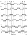
- FIG. 4 shows time profiles of drive signals U USTU1 , U USTU2 U VSTU1 , U VSTU2 U WSTU1 , U WSTU2 of the first and second partial converter TU1, TU2 for all three converter phases U, V, W, in FIG and FIG.
- FIG. 4 shows the first drive signal sequence PM1 and the inverted first drive signal sequence invPM1 "line-hatched” for clarity and the second drive signal sequence PM 2 and the inverted second drive signal sequence invPM2 "crosshatched”.
- first for a first converter phase u at time (2n) .tau the first partial converter TU1 is replaced by a first drive signal sequence PM1 and at the time (2n + 1).
- ⁇ T for the duration T driven by a second drive signal sequence PM2, where n 0, 1, 2, 3, ... and T is a period of the phase voltage U u of the first converter phase u.
- the second partial converter TU2 is replaced by the inverted second drive signal sequence invPM2 and at time (2n + 1) * T for the time T by the inverted first drive signal sequence invPM1 controlled.
- the first partial converter TU1 is triggered by the first control signal sequence PM1 and at the time (2n + 5/3) ⁇ T for the period T driven by the second drive signal sequence PM2.
- the second partial converter TU2 passes through the inverted second drive signal sequence invPM2 and at the time (2n + 5/3) ⁇ T for the time period T, respectively the inverted first drive signal sequence invPM1 driven.
- the activation ensures that the power semiconductor switches of the respective partial converter TU1, TU2 are switched such that the respective partial converter phase according to FIG.
- a third converter phase v at the time (2n + 1/3) ⁇ T for the time period T of the first partial converter TU1 by the second drive signal sequence PM2 and the second partial converter TU2 is driven by the inverted first drive signal sequence invPM1. Furthermore, for the third converter phase v at the time (2n + 4/3) ⁇ T for the time period T of the first partial converter TU1 by the first drive signal sequence PM1 and the second partial converter TU2 is driven by the inverted second drive signal sequence invPM2.
- the first drive signal sequence PM1, the inverted first drive signal sequence invPM1, the second drive signal sequence PM2 and the inverted second drive signal sequence invPM2 preferably each have an expiration duration corresponding to the time duration T, ie the period of the first converter phase voltage U u .
- the first partial converter TU1 is provided by the second drive signal sequence PM2 and the second partial converter TU2 by the inverted first drive signal sequence invPM1 and further at the time (2n + 4/3) ⁇ T the first partial converter TU1 is driven by the first drive signal sequence PM1 and the second partial converter TU2 is driven by the inverted second drive signal sequence invPM2, it is possible to achieve oscillations in the respective DC voltage circuit 1 of the corresponding subcircuit TU1, TU2 can be reduced.
- FIG. 6 shows such a vibration for the method according to the invention for operating the converter circuit according to FIG. 1, FIG. 6 showing time profiles of the partial voltages U TU1DC1 , U TU1DC2 at the two capacitors C 1 , C 2 of the DC voltage circuit 1 of the first Subconductor TU1 and time courses of the partial voltages U TU2DC1 , U TU2DC2 are shown at the two capacitors C 1 , C 2 of the DC voltage circuit 1 of the second partial converter TU2.
- the drive signal sequences PM1, PM2, invPM1, invPM2 is achieved that the switching losses and the conduction losses evenly on the power semiconductor switches of the two partial converter TU1, TU2, whereby the converter circuit with respect to the semiconductor temperatures can be operated at maximum power.
- the refer both partial converter TU1, TU2 due to the cyclic exchange of the drive signal sequences PM1, PM2, invPM1, invPM2 essentially the same power, for example, from a connected electrical supply network, causing the two DC voltage circuits 1 stationary substantially the same voltage.
- first, second and third converter phase u, v, w with the respectively associated first, second and third converter phase voltage U u , U v , U w is purely arbitrary and is not subject to any restrictions ,
- the first converter phase could also have been designated w, the second converter phase v and the third converter phase u.
- the inventive method for operating a three-phase converter circuit an extremely simple solution, which is therefore easy to implement and existing Easy to implement inverter circuits. Furthermore, the inventive Method due to its simplicity cost-effective yet highly efficient.
Landscapes
- Engineering & Computer Science (AREA)
- Power Engineering (AREA)
- Inverter Devices (AREA)
- Dc-Dc Converters (AREA)
- Power Conversion In General (AREA)
Abstract
Description
- Fig. 1
- eine gängige Ausführungsform einer dreiphasigen Umrichterschaltung,
- Fig. 2
- typischer zeitlicher Verlauf eines Ansteuersignals des ersten und zweiten Teilumrichters, einer Teilumrichterphasenspannung des ersten und zweiten Teilumrichters und einer Umrichterphasenspannung,
- Fig. 3
- typische zeitliche Verläufe von Ansteuersignalen des ersten und zweiten Teilumrichters für alle drei Umrichterphasen,
- Fig. 4
- zeitliche Verläufe von erfindungsgemässen Ansteuersignalen des ersten und zweiten Teilumrichters für alle drei Umrichterphasen,
- Fig. 5
- typische zeitliche Verläufe von Teilgleichspannungen der Gleichspannungskreise des ersten und zweiten Teilumrichters und
- Fig. 6
- zeitliche Verläufe nach der Erfindung von Teilgleichspannungen der Gleichspannungskreise des ersten und zweiten Teilumrichters.
- 1
- Gleichspannungskreis
- 2
- erste Spannungsreduziereinrichtung
- 3
- zweite Spannungsreduziereinrichtung
- 4
- Schaltsystem
- 5
- erste Schaltgruppe
- 6
- zweite Schaltgruppe
- 7
- dritte Schaltgruppe
Claims (2)
- Verfahren zum Betrieb einer dreiphasigen Umrichterschaltung, bei dem für eine erste Umrichterphase (u) jeweils zum Zeitpunkt (2n)·T für die Zeitdauer T der erste Teilumrichter (TU1) durch eine erste Ansteuersignalabfolge (PM1) und jeweils zum Zeitpunkt (2n+1)·T für die Zeitdauer T durch eine zweite Ansteuersignalabfolge (PM2) angesteuert wird,
bei dem für die erste Umrichterphase (u) jeweils zum Zeitpunkt (2n)·T für die Zeitdauer T der zweite Teilumrichter (TU2) durch die invertierte zweite Ansteuersignalabfolge (invPM2) und jeweils zum Zeitpunkt (2n +1)·T für die Zeitdauer T durch die invertierte erste Ansteuersignalabfolge (invPM1) angesteuert wird,
bei dem für eine zweite Umrichterphase (w) jeweils zum Zeitpunkt (2n+ 2 / 3)·T für die Zeitdauer T der erste Teilumrichter (TU1) durch die erste Ansteuersignalabfolge (PM1) und jeweils zum Zeitpunkt (2n + 5 / 3)·T für die Zeitdauer T durch die zweite Ansteuersignalabfolge (PM2) angesteuert wird, und bei dem für die zweite Umrichterphase (w) jeweils zum Zeitpunkt (2n+ 2 / 3)·T für die Zeitdauer T der zweite Teilumrichter (TU2) durch die invertierte zweite Ansteuersignalabfolge (invPM2) und jeweils zum Zeitpunkt (2n+ 5 / 3)·T für die Zeitdauer T durch die invertierte erste Ansteuersignalabfolge (invPM1) angesteuert, wobei n=0, 1, 2, 3,... ist und T eine Periodendauer der Phasenspannung (Uu) der ersten Umrichterphase (u) ist, dadurch gekennzeichnet, dass für eine dritte Umrichterphase (v) jeweils zum Zeitpunkt (2n+ 1 / 3)·T für die Zeitdauer T der erste Teilumrichter (TU1) durch die zweite Ansteuersignalabfolge (PM2) und der zweite Teilumrichter (TU2) durch die invertierte erste Ansteuersignalabfolge (invPM1) angesteuert wird, und
dass für die dritte Umrichterphase (v) jeweils zum Zeitpunkt (2n+ 4 / 3)·T für die Zeitdauer T der erste Teilumrichter (TU1) durch die erste Ansteuersignalabfolge (PM1) und der zweite Teilumrichter (TU1) durch die invertierte zweite Ansteuersignalabfolge (invPm2) angesteuert wird. - Verfahren nach Anspruch 1, dadurch gekennzeichnet, dass die erste Ansteuersignalabfolge (PM1), die invertierte erste Ansteuersignalabfolge (invPM1), die zweite Ansteuersignalabfolge (PM2) und die invertierte zweite Ansteuersignalabfolge (invPM2) jeweils eine Ablaufdauer aufweisen, die der Zeitdauer T entspricht.
Priority Applications (3)
| Application Number | Priority Date | Filing Date | Title |
|---|---|---|---|
| EP03405668A EP1515421B1 (de) | 2003-09-12 | 2003-09-12 | Verfahren zum Betrieb einer dreiphasigen Umrichterschaltung |
| AT03405668T ATE437468T1 (de) | 2003-09-12 | 2003-09-12 | Verfahren zum betrieb einer dreiphasigen umrichterschaltung |
| DE50311733T DE50311733D1 (de) | 2003-09-12 | 2003-09-12 | Verfahren zum Betrieb einer dreiphasigen Umrichterschaltung |
Applications Claiming Priority (1)
| Application Number | Priority Date | Filing Date | Title |
|---|---|---|---|
| EP03405668A EP1515421B1 (de) | 2003-09-12 | 2003-09-12 | Verfahren zum Betrieb einer dreiphasigen Umrichterschaltung |
Publications (2)
| Publication Number | Publication Date |
|---|---|
| EP1515421A1 true EP1515421A1 (de) | 2005-03-16 |
| EP1515421B1 EP1515421B1 (de) | 2009-07-22 |
Family
ID=34130414
Family Applications (1)
| Application Number | Title | Priority Date | Filing Date |
|---|---|---|---|
| EP03405668A Expired - Lifetime EP1515421B1 (de) | 2003-09-12 | 2003-09-12 | Verfahren zum Betrieb einer dreiphasigen Umrichterschaltung |
Country Status (3)
| Country | Link |
|---|---|
| EP (1) | EP1515421B1 (de) |
| AT (1) | ATE437468T1 (de) |
| DE (1) | DE50311733D1 (de) |
Citations (2)
| Publication number | Priority date | Publication date | Assignee | Title |
|---|---|---|---|---|
| US4392099A (en) * | 1979-02-20 | 1983-07-05 | Tokyo Shibaura Denki Kabushiki Kaisha | Starting system for brushless motor |
| EP0534242A1 (de) * | 1991-09-24 | 1993-03-31 | Siemens Aktiengesellschaft | Verfahren zur Reduzierung von Spannungsschwingungen eines Zwischenkreismittenanschlusses eines Dreipunktumrichters |
-
2003
- 2003-09-12 AT AT03405668T patent/ATE437468T1/de not_active IP Right Cessation
- 2003-09-12 DE DE50311733T patent/DE50311733D1/de not_active Expired - Lifetime
- 2003-09-12 EP EP03405668A patent/EP1515421B1/de not_active Expired - Lifetime
Patent Citations (2)
| Publication number | Priority date | Publication date | Assignee | Title |
|---|---|---|---|---|
| US4392099A (en) * | 1979-02-20 | 1983-07-05 | Tokyo Shibaura Denki Kabushiki Kaisha | Starting system for brushless motor |
| EP0534242A1 (de) * | 1991-09-24 | 1993-03-31 | Siemens Aktiengesellschaft | Verfahren zur Reduzierung von Spannungsschwingungen eines Zwischenkreismittenanschlusses eines Dreipunktumrichters |
Non-Patent Citations (3)
| Title |
|---|
| HAORAN ZHANG ET AL: "A reduced switch dual-bridge inverter topology for the mitigation of bearing currents, EMI and DC-link voltage variations", INDUSTRY APPLICATIONS CONFERENCE, 1999. THIRTY-FOURTH IAS ANNUAL MEETING. CONFERENCE RECORD OF THE 1999 IEEE PHOENIX, AZ, USA 3-7 OCT. 1999, PISCATAWAY, NJ, USA,IEEE, US, 3 October 1999 (1999-10-03), pages 1945 - 1949, XP010355130, ISBN: 0-7803-5589-X * |
| VON JOUANNE A ; HAORAN ZHANG: "A Dual-Bridge Inverter Approach to Eliminating Common-Mode Voltages and Bearing and Leakage Currents", IEEE TRANSACTIONS ON POWER ELECTRONICS, vol. 14, no. 1, January 1999 (1999-01-01), pages 43 - 48, XP002270967, ISBN: 0885-8993 * |
| YO-HAN LEE; RAE-YOUNG KIM; DONG-SEOK HYUN: "A novel SVPWM Strategy Considering DC-link Balancing for a Multi-level Voltage Source Inverter", APEC '99. FOURTEENTH ANNUAL APPLIED POWER ELECTRONICS CONFERENCE AND EXPOSITION. 1999 CONFERENCE PROCEEDINGS (CAT. NO.99CH36285), PROCEEDINGS OF APEC '99 - APPLIED POWER ELECTRONICS CONFERENCE, DALLAS, TX, USA, 14-18 MARCH 1999, 14 March 1999 (1999-03-14), pages 509 - 514, XP002270968, ISBN: 0-7803-5160-6 * |
Also Published As
| Publication number | Publication date |
|---|---|
| ATE437468T1 (de) | 2009-08-15 |
| DE50311733D1 (de) | 2009-09-03 |
| EP1515421B1 (de) | 2009-07-22 |
Similar Documents
| Publication | Publication Date | Title |
|---|---|---|
| DE69722756T2 (de) | Leistungswandler mit verbesserter Hauptschaltersteuerung und mehreren Spannungspegeln | |
| EP2709257A2 (de) | Stromrichterschaltung und Verfahren zur Steuerung der Stromrichterschaltung | |
| DE102020000402A1 (de) | Techniken für mehrphasige schaltende Kondensator-Spule Aufwärtswandler | |
| EP1459434B1 (de) | Schaltungsanordnung zum betreiben einer elektrischen maschine | |
| DE69619648T2 (de) | Verfahren zur Steuerung eines Leistungswandlers | |
| EP0884831A2 (de) | Verfahren zum Betrieb einer leistungselektronischen Schaltungsanordnung | |
| WO2007054149A1 (de) | Schaltungsanordnung und ein verfahren zur galvanisch getrennten ansteuerung eines halbleiterschalters | |
| CH644476A5 (de) | Leistungswechselrichter. | |
| DE2106310A1 (de) | Mehrphasen Leistungskonverterschaltung | |
| DE19961382A1 (de) | Elektrische Schaltung, insbesondere für einen Mittelspannungsstromrichter | |
| DE69127808T2 (de) | Stromregler für induktive last | |
| DE69226056T2 (de) | Verfahren und Treiber für Feldeffekt-Leistungsschalter mit einer aufgefrischten, ein stabiles Ein-/Ausschalten sicherstellenden Spannungsversorgung | |
| DE10000020A1 (de) | Integrierte Gate-Treiberschaltung | |
| EP2251979A1 (de) | Verfahren und Treiberschaltung zum Treiben eines Halbleiterleistungsschalters | |
| DE2461583C2 (de) | Schaltung zur Reduzierung der Einschaltverluste eines Leistungstransistors | |
| EP1513249A1 (de) | Verfahren zur Symmetrierung eines Gleichspannungskreises einer Umrichterschaltung zur Schaltung von drei Spannungsniveaus | |
| DE19825801C2 (de) | Gleichspannungs-Zwischenkreis mit Hochlast-Widerstand | |
| DE68905238T2 (de) | Linearisierungsverfahren fuer gleichspannungswandler und durchfuehrung des verfahrens. | |
| EP2254233B1 (de) | Verfahren zum Betrieb einer Umrichterschaltung sowie Vorrichtung zur Durchführung des Verfahrens | |
| EP1515421A1 (de) | Verfahren zum Betrieb einer dreiphasigen Umrichterschaltung | |
| DE102006060828A1 (de) | Umrichter mit einer Verzögerungsschaltung für PWM-Signale | |
| DE19812069A1 (de) | Leistungsverstärker und Verfahren zum Erzeugen von Steuersignalen für einen Leistungsverstärker | |
| EP2375551B1 (de) | Kommutierungsverfahren, Kommutierungsschaltung und elektrischer Energiewandler | |
| DE102019135718A1 (de) | Wechselrichter und Verfahren zum Betreiben eines Wechselrichters | |
| DE102020200672A1 (de) | Galvanisch getrenntes energietechnisches Koppeln von wenigstens zweipoligen Energieversorgungsleitungen |
Legal Events
| Date | Code | Title | Description |
|---|---|---|---|
| PUAI | Public reference made under article 153(3) epc to a published international application that has entered the european phase |
Free format text: ORIGINAL CODE: 0009012 |
|
| AK | Designated contracting states |
Kind code of ref document: A1 Designated state(s): AT BE BG CH CY CZ DE DK EE ES FI FR GB GR HU IE IT LI LU MC NL PT RO SE SI SK TR |
|
| AX | Request for extension of the european patent |
Extension state: AL LT LV MK |
|
| 17P | Request for examination filed |
Effective date: 20050818 |
|
| AKX | Designation fees paid |
Designated state(s): AT BE BG CH CY CZ DE DK EE ES FI FR GB GR HU IE IT LI LU MC NL PT RO SE SI SK TR |
|
| GRAP | Despatch of communication of intention to grant a patent |
Free format text: ORIGINAL CODE: EPIDOSNIGR1 |
|
| RIN1 | Information on inventor provided before grant (corrected) |
Inventor name: SARIO, PETTERI Inventor name: GERHARD, BILAL Inventor name: HEROLD, SIMON |
|
| GRAS | Grant fee paid |
Free format text: ORIGINAL CODE: EPIDOSNIGR3 |
|
| GRAA | (expected) grant |
Free format text: ORIGINAL CODE: 0009210 |
|
| AK | Designated contracting states |
Kind code of ref document: B1 Designated state(s): AT BE BG CH CY CZ DE DK EE ES FI FR GB GR HU IE IT LI LU MC NL PT RO SE SI SK TR |
|
| REG | Reference to a national code |
Ref country code: GB Ref legal event code: FG4D Free format text: NOT ENGLISH |
|
| REG | Reference to a national code |
Ref country code: CH Ref legal event code: EP |
|
| REG | Reference to a national code |
Ref country code: IE Ref legal event code: FG4D |
|
| REF | Corresponds to: |
Ref document number: 50311733 Country of ref document: DE Date of ref document: 20090903 Kind code of ref document: P |
|
| REG | Reference to a national code |
Ref country code: CH Ref legal event code: NV Representative=s name: ABB SCHWEIZ AG INTELLECTUAL PROPERTY (CH-LC/IP) |
|
| NLV1 | Nl: lapsed or annulled due to failure to fulfill the requirements of art. 29p and 29m of the patents act | ||
| PG25 | Lapsed in a contracting state [announced via postgrant information from national office to epo] |
Ref country code: SE Free format text: LAPSE BECAUSE OF FAILURE TO SUBMIT A TRANSLATION OF THE DESCRIPTION OR TO PAY THE FEE WITHIN THE PRESCRIBED TIME-LIMIT Effective date: 20090722 Ref country code: ES Free format text: LAPSE BECAUSE OF FAILURE TO SUBMIT A TRANSLATION OF THE DESCRIPTION OR TO PAY THE FEE WITHIN THE PRESCRIBED TIME-LIMIT Effective date: 20091102 Ref country code: FI Free format text: LAPSE BECAUSE OF FAILURE TO SUBMIT A TRANSLATION OF THE DESCRIPTION OR TO PAY THE FEE WITHIN THE PRESCRIBED TIME-LIMIT Effective date: 20090722 |
|
| PG25 | Lapsed in a contracting state [announced via postgrant information from national office to epo] |
Ref country code: SI Free format text: LAPSE BECAUSE OF FAILURE TO SUBMIT A TRANSLATION OF THE DESCRIPTION OR TO PAY THE FEE WITHIN THE PRESCRIBED TIME-LIMIT Effective date: 20090722 Ref country code: NL Free format text: LAPSE BECAUSE OF FAILURE TO SUBMIT A TRANSLATION OF THE DESCRIPTION OR TO PAY THE FEE WITHIN THE PRESCRIBED TIME-LIMIT Effective date: 20090722 |
|
| REG | Reference to a national code |
Ref country code: IE Ref legal event code: FD4D |
|
| BERE | Be: lapsed |
Owner name: ABB RESEARCH LTD. Effective date: 20090930 |
|
| PG25 | Lapsed in a contracting state [announced via postgrant information from national office to epo] |
Ref country code: PT Free format text: LAPSE BECAUSE OF FAILURE TO SUBMIT A TRANSLATION OF THE DESCRIPTION OR TO PAY THE FEE WITHIN THE PRESCRIBED TIME-LIMIT Effective date: 20091122 Ref country code: BG Free format text: LAPSE BECAUSE OF FAILURE TO SUBMIT A TRANSLATION OF THE DESCRIPTION OR TO PAY THE FEE WITHIN THE PRESCRIBED TIME-LIMIT Effective date: 20091022 |
|
| PG25 | Lapsed in a contracting state [announced via postgrant information from national office to epo] |
Ref country code: IE Free format text: LAPSE BECAUSE OF FAILURE TO SUBMIT A TRANSLATION OF THE DESCRIPTION OR TO PAY THE FEE WITHIN THE PRESCRIBED TIME-LIMIT Effective date: 20090722 Ref country code: RO Free format text: LAPSE BECAUSE OF FAILURE TO SUBMIT A TRANSLATION OF THE DESCRIPTION OR TO PAY THE FEE WITHIN THE PRESCRIBED TIME-LIMIT Effective date: 20090722 Ref country code: MC Free format text: LAPSE BECAUSE OF NON-PAYMENT OF DUE FEES Effective date: 20090930 Ref country code: EE Free format text: LAPSE BECAUSE OF FAILURE TO SUBMIT A TRANSLATION OF THE DESCRIPTION OR TO PAY THE FEE WITHIN THE PRESCRIBED TIME-LIMIT Effective date: 20090722 Ref country code: DK Free format text: LAPSE BECAUSE OF FAILURE TO SUBMIT A TRANSLATION OF THE DESCRIPTION OR TO PAY THE FEE WITHIN THE PRESCRIBED TIME-LIMIT Effective date: 20090722 Ref country code: CZ Free format text: LAPSE BECAUSE OF FAILURE TO SUBMIT A TRANSLATION OF THE DESCRIPTION OR TO PAY THE FEE WITHIN THE PRESCRIBED TIME-LIMIT Effective date: 20090722 |
|
| PLBE | No opposition filed within time limit |
Free format text: ORIGINAL CODE: 0009261 |
|
| STAA | Information on the status of an ep patent application or granted ep patent |
Free format text: STATUS: NO OPPOSITION FILED WITHIN TIME LIMIT |
|
| PG25 | Lapsed in a contracting state [announced via postgrant information from national office to epo] |
Ref country code: SK Free format text: LAPSE BECAUSE OF FAILURE TO SUBMIT A TRANSLATION OF THE DESCRIPTION OR TO PAY THE FEE WITHIN THE PRESCRIBED TIME-LIMIT Effective date: 20090722 |
|
| 26N | No opposition filed |
Effective date: 20100423 |
|
| PG25 | Lapsed in a contracting state [announced via postgrant information from national office to epo] |
Ref country code: BE Free format text: LAPSE BECAUSE OF NON-PAYMENT OF DUE FEES Effective date: 20090930 |
|
| PG25 | Lapsed in a contracting state [announced via postgrant information from national office to epo] |
Ref country code: GR Free format text: LAPSE BECAUSE OF FAILURE TO SUBMIT A TRANSLATION OF THE DESCRIPTION OR TO PAY THE FEE WITHIN THE PRESCRIBED TIME-LIMIT Effective date: 20091023 |
|
| PG25 | Lapsed in a contracting state [announced via postgrant information from national office to epo] |
Ref country code: AT Free format text: LAPSE BECAUSE OF NON-PAYMENT OF DUE FEES Effective date: 20090912 |
|
| PG25 | Lapsed in a contracting state [announced via postgrant information from national office to epo] |
Ref country code: LU Free format text: LAPSE BECAUSE OF NON-PAYMENT OF DUE FEES Effective date: 20090912 |
|
| PG25 | Lapsed in a contracting state [announced via postgrant information from national office to epo] |
Ref country code: HU Free format text: LAPSE BECAUSE OF FAILURE TO SUBMIT A TRANSLATION OF THE DESCRIPTION OR TO PAY THE FEE WITHIN THE PRESCRIBED TIME-LIMIT Effective date: 20100123 |
|
| PG25 | Lapsed in a contracting state [announced via postgrant information from national office to epo] |
Ref country code: TR Free format text: LAPSE BECAUSE OF FAILURE TO SUBMIT A TRANSLATION OF THE DESCRIPTION OR TO PAY THE FEE WITHIN THE PRESCRIBED TIME-LIMIT Effective date: 20090722 |
|
| PG25 | Lapsed in a contracting state [announced via postgrant information from national office to epo] |
Ref country code: CY Free format text: LAPSE BECAUSE OF FAILURE TO SUBMIT A TRANSLATION OF THE DESCRIPTION OR TO PAY THE FEE WITHIN THE PRESCRIBED TIME-LIMIT Effective date: 20090722 |
|
| PGFP | Annual fee paid to national office [announced via postgrant information from national office to epo] |
Ref country code: DE Payment date: 20140922 Year of fee payment: 12 Ref country code: CH Payment date: 20140919 Year of fee payment: 12 |
|
| PGFP | Annual fee paid to national office [announced via postgrant information from national office to epo] |
Ref country code: FR Payment date: 20140919 Year of fee payment: 12 Ref country code: GB Payment date: 20140919 Year of fee payment: 12 |
|
| PGFP | Annual fee paid to national office [announced via postgrant information from national office to epo] |
Ref country code: IT Payment date: 20140923 Year of fee payment: 12 |
|
| REG | Reference to a national code |
Ref country code: DE Ref legal event code: R119 Ref document number: 50311733 Country of ref document: DE |
|
| PG25 | Lapsed in a contracting state [announced via postgrant information from national office to epo] |
Ref country code: IT Free format text: LAPSE BECAUSE OF NON-PAYMENT OF DUE FEES Effective date: 20150912 |
|
| REG | Reference to a national code |
Ref country code: CH Ref legal event code: PL |
|
| GBPC | Gb: european patent ceased through non-payment of renewal fee |
Effective date: 20150912 |
|
| REG | Reference to a national code |
Ref country code: FR Ref legal event code: ST Effective date: 20160531 |
|
| PG25 | Lapsed in a contracting state [announced via postgrant information from national office to epo] |
Ref country code: LI Free format text: LAPSE BECAUSE OF NON-PAYMENT OF DUE FEES Effective date: 20150930 Ref country code: DE Free format text: LAPSE BECAUSE OF NON-PAYMENT OF DUE FEES Effective date: 20160401 Ref country code: GB Free format text: LAPSE BECAUSE OF NON-PAYMENT OF DUE FEES Effective date: 20150912 Ref country code: CH Free format text: LAPSE BECAUSE OF NON-PAYMENT OF DUE FEES Effective date: 20150930 |
|
| PG25 | Lapsed in a contracting state [announced via postgrant information from national office to epo] |
Ref country code: FR Free format text: LAPSE BECAUSE OF NON-PAYMENT OF DUE FEES Effective date: 20150930 |