EP1515269A2 - An integrated circuit card and a method of manufacturing the same - Google Patents
An integrated circuit card and a method of manufacturing the same Download PDFInfo
- Publication number
- EP1515269A2 EP1515269A2 EP04254322A EP04254322A EP1515269A2 EP 1515269 A2 EP1515269 A2 EP 1515269A2 EP 04254322 A EP04254322 A EP 04254322A EP 04254322 A EP04254322 A EP 04254322A EP 1515269 A2 EP1515269 A2 EP 1515269A2
- Authority
- EP
- European Patent Office
- Prior art keywords
- tape substrate
- molding resin
- plug
- chip
- card
- Prior art date
- Legal status (The legal status is an assumption and is not a legal conclusion. Google has not performed a legal analysis and makes no representation as to the accuracy of the status listed.)
- Withdrawn
Links
Images










Classifications
-
- G—PHYSICS
- G06—COMPUTING OR CALCULATING; COUNTING
- G06K—GRAPHICAL DATA READING; PRESENTATION OF DATA; RECORD CARRIERS; HANDLING RECORD CARRIERS
- G06K19/00—Record carriers for use with machines and with at least a part designed to carry digital markings
- G06K19/06—Record carriers for use with machines and with at least a part designed to carry digital markings characterised by the kind of the digital marking, e.g. shape, nature, code
- G06K19/067—Record carriers with conductive marks, printed circuits or semiconductor circuit elements, e.g. credit or identity cards also with resonating or responding marks without active components
- G06K19/07—Record carriers with conductive marks, printed circuits or semiconductor circuit elements, e.g. credit or identity cards also with resonating or responding marks without active components with integrated circuit chips
- G06K19/077—Constructional details, e.g. mounting of circuits in the carrier
- G06K19/07745—Mounting details of integrated circuit chips
-
- G—PHYSICS
- G06—COMPUTING OR CALCULATING; COUNTING
- G06K—GRAPHICAL DATA READING; PRESENTATION OF DATA; RECORD CARRIERS; HANDLING RECORD CARRIERS
- G06K19/00—Record carriers for use with machines and with at least a part designed to carry digital markings
- G06K19/06—Record carriers for use with machines and with at least a part designed to carry digital markings characterised by the kind of the digital marking, e.g. shape, nature, code
- G06K19/067—Record carriers with conductive marks, printed circuits or semiconductor circuit elements, e.g. credit or identity cards also with resonating or responding marks without active components
- G06K19/07—Record carriers with conductive marks, printed circuits or semiconductor circuit elements, e.g. credit or identity cards also with resonating or responding marks without active components with integrated circuit chips
- G06K19/077—Constructional details, e.g. mounting of circuits in the carrier
-
- G—PHYSICS
- G06—COMPUTING OR CALCULATING; COUNTING
- G06K—GRAPHICAL DATA READING; PRESENTATION OF DATA; RECORD CARRIERS; HANDLING RECORD CARRIERS
- G06K19/00—Record carriers for use with machines and with at least a part designed to carry digital markings
- G06K19/06—Record carriers for use with machines and with at least a part designed to carry digital markings characterised by the kind of the digital marking, e.g. shape, nature, code
- G06K19/067—Record carriers with conductive marks, printed circuits or semiconductor circuit elements, e.g. credit or identity cards also with resonating or responding marks without active components
- G06K19/07—Record carriers with conductive marks, printed circuits or semiconductor circuit elements, e.g. credit or identity cards also with resonating or responding marks without active components with integrated circuit chips
- G06K19/077—Constructional details, e.g. mounting of circuits in the carrier
- G06K19/07718—Constructional details, e.g. mounting of circuits in the carrier the record carrier being manufactured in a continuous process, e.g. using endless rolls
-
- G—PHYSICS
- G06—COMPUTING OR CALCULATING; COUNTING
- G06K—GRAPHICAL DATA READING; PRESENTATION OF DATA; RECORD CARRIERS; HANDLING RECORD CARRIERS
- G06K19/00—Record carriers for use with machines and with at least a part designed to carry digital markings
- G06K19/06—Record carriers for use with machines and with at least a part designed to carry digital markings characterised by the kind of the digital marking, e.g. shape, nature, code
- G06K19/067—Record carriers with conductive marks, printed circuits or semiconductor circuit elements, e.g. credit or identity cards also with resonating or responding marks without active components
- G06K19/07—Record carriers with conductive marks, printed circuits or semiconductor circuit elements, e.g. credit or identity cards also with resonating or responding marks without active components with integrated circuit chips
- G06K19/077—Constructional details, e.g. mounting of circuits in the carrier
- G06K19/0772—Physical layout of the record carrier
- G06K19/07724—Physical layout of the record carrier the record carrier being at least partially made by a molding process
-
- G—PHYSICS
- G06—COMPUTING OR CALCULATING; COUNTING
- G06K—GRAPHICAL DATA READING; PRESENTATION OF DATA; RECORD CARRIERS; HANDLING RECORD CARRIERS
- G06K19/00—Record carriers for use with machines and with at least a part designed to carry digital markings
- G06K19/06—Record carriers for use with machines and with at least a part designed to carry digital markings characterised by the kind of the digital marking, e.g. shape, nature, code
- G06K19/067—Record carriers with conductive marks, printed circuits or semiconductor circuit elements, e.g. credit or identity cards also with resonating or responding marks without active components
- G06K19/07—Record carriers with conductive marks, printed circuits or semiconductor circuit elements, e.g. credit or identity cards also with resonating or responding marks without active components with integrated circuit chips
- G06K19/077—Constructional details, e.g. mounting of circuits in the carrier
- G06K19/0772—Physical layout of the record carrier
- G06K19/07733—Physical layout of the record carrier the record carrier containing at least one further contact interface not conform ISO-7816
-
- G—PHYSICS
- G06—COMPUTING OR CALCULATING; COUNTING
- G06K—GRAPHICAL DATA READING; PRESENTATION OF DATA; RECORD CARRIERS; HANDLING RECORD CARRIERS
- G06K19/00—Record carriers for use with machines and with at least a part designed to carry digital markings
- G06K19/06—Record carriers for use with machines and with at least a part designed to carry digital markings characterised by the kind of the digital marking, e.g. shape, nature, code
- G06K19/067—Record carriers with conductive marks, printed circuits or semiconductor circuit elements, e.g. credit or identity cards also with resonating or responding marks without active components
- G06K19/07—Record carriers with conductive marks, printed circuits or semiconductor circuit elements, e.g. credit or identity cards also with resonating or responding marks without active components with integrated circuit chips
- G06K19/077—Constructional details, e.g. mounting of circuits in the carrier
- G06K19/07743—External electrical contacts
-
- H—ELECTRICITY
- H10—SEMICONDUCTOR DEVICES; ELECTRIC SOLID-STATE DEVICES NOT OTHERWISE PROVIDED FOR
- H10W—GENERIC PACKAGES, INTERCONNECTIONS, CONNECTORS OR OTHER CONSTRUCTIONAL DETAILS OF DEVICES COVERED BY CLASS H10
- H10W72/00—Interconnections or connectors in packages
- H10W72/071—Connecting or disconnecting
- H10W72/075—Connecting or disconnecting of bond wires
- H10W72/07551—Connecting or disconnecting of bond wires characterised by changes in properties of the bond wires during the connecting
- H10W72/07554—Connecting or disconnecting of bond wires characterised by changes in properties of the bond wires during the connecting changes in dispositions
-
- H—ELECTRICITY
- H10—SEMICONDUCTOR DEVICES; ELECTRIC SOLID-STATE DEVICES NOT OTHERWISE PROVIDED FOR
- H10W—GENERIC PACKAGES, INTERCONNECTIONS, CONNECTORS OR OTHER CONSTRUCTIONAL DETAILS OF DEVICES COVERED BY CLASS H10
- H10W72/00—Interconnections or connectors in packages
- H10W72/50—Bond wires
- H10W72/541—Dispositions of bond wires
- H10W72/547—Dispositions of multiple bond wires
-
- H—ELECTRICITY
- H10—SEMICONDUCTOR DEVICES; ELECTRIC SOLID-STATE DEVICES NOT OTHERWISE PROVIDED FOR
- H10W—GENERIC PACKAGES, INTERCONNECTIONS, CONNECTORS OR OTHER CONSTRUCTIONAL DETAILS OF DEVICES COVERED BY CLASS H10
- H10W72/00—Interconnections or connectors in packages
- H10W72/50—Bond wires
- H10W72/551—Materials of bond wires
- H10W72/552—Materials of bond wires comprising metals or metalloids, e.g. silver
- H10W72/5522—Materials of bond wires comprising metals or metalloids, e.g. silver comprising gold [Au]
-
- H—ELECTRICITY
- H10—SEMICONDUCTOR DEVICES; ELECTRIC SOLID-STATE DEVICES NOT OTHERWISE PROVIDED FOR
- H10W—GENERIC PACKAGES, INTERCONNECTIONS, CONNECTORS OR OTHER CONSTRUCTIONAL DETAILS OF DEVICES COVERED BY CLASS H10
- H10W90/00—Package configurations
- H10W90/701—Package configurations characterised by the relative positions of pads or connectors relative to package parts
- H10W90/751—Package configurations characterised by the relative positions of pads or connectors relative to package parts of bond wires
- H10W90/754—Package configurations characterised by the relative positions of pads or connectors relative to package parts of bond wires between a chip and a stacked insulating package substrate, interposer or RDL
Definitions
- the present invention relates to an integrated circuit (IC) card and a method of manufacturing the same. Particularly, the present invention is concerned with a technique effectively applicable to a plug-in universal IC card for a portable telephone.
- IC integrated circuit
- GSM Global System for Mobile Communications
- SIM Subscriber Identity Module
- IMT-2000 International Mobile Telecommunication 2000
- IMT-2000 International Mobile Telecommunication 2000
- IMT-2000 International Mobile Telecommunication 2000
- a universal IC card (UICC; Plug-in Universal Integrated Circuit Card) which is an upward compatible card having an extended function from the function of the SIM card.
- UICC Plug-in Universal Integrated Circuit Card
- universal IC cards there are a plug-in type and a standard IC card type which is larger in size.
- Patent Literature 1 discloses an improved technique for a plug-in SIM card.
- the plug-in SIM card is shipped in a fixed state to a part of a frame card having a standard IC card size, then when to be used, it is cut off from the frame card and is inserted into a portable telephone, while the frame card which has become unnecessary is discharged to waste.
- discarding the frame card is not desirable from the standpoint of resources saving and environment conservation.
- Patent Literature 1 proposes a technique that a magnetic storage portion is provided in part of the plug-in SIM card and various pieces of information heretofore printed on the surface of the frame card are stored in the magnetic storage portion, thereby making the frame card unnecessary.
- the plug-in SIM card used in a portable telephone based on GSM system has a construction wherein a semiconductor chip (hereinafter referred to simply as "chip") is embedded in a resinous plug-in card having an external dimension of 15 mm long, 25 mm wide and 0.76 mm thick.
- chip a semiconductor chip
- the above chip is mounted on one side of a thin tape substrate having a thickness of about 160 mm and is sealed with a potting resin.
- a cavity for embedding the resin-sealed chip therein.
- the substrate is cut in conformity with the shape of the cavity and is then affixed to the plug-in card, whereby the chip is embedded in the cavity.
- contact patterns external terminals which are connected to the chip through Au wires.
- the plug-in universal IC card (plug-in UICC" hereinafter) used in IMT-2000 system, according to the specification thereof, is constructed to have the same external dimension as the plug-in SIM card.
- plug-in UICC plug-in universal IC card
- an increase in size of the chip incorporated in the card or a multi-chip structure is required.
- the existing plug-in SIM cards having the above-mentioned structure however, it turned out through studies made by the present inventors that mounting a large-sized chip or implementing a multi-chip structure was difficult for the following reason.
- the resin is injected into a cavity while the tape substrate is pinched between an upper die half and a lower die half of a molding die.
- outer periphery ends of a mold cavity formed in the upper die half be positioned about 2 mm inside outer periphery ends of contact patterns formed on a back surface of the tape substrate. This is because if the aforesaid size is smaller at the time of pinching the tape substrate between the upper and lower die halves, an excessive pressure is exerted on the outer periphery ends of the contact patterns and consequently the surfaces of the contact patterns are impressed by the die, which causes a poor appearance.
- the plug-in SIM card since the volume of the cavity in the plug-in card is limited, it is difficult to mount a large-sized chip or increase the number of chips. Accordingly, in the case where the plug-in SIM card of the conventional structure is applied to a plug-in UICC, it is difficult to expand the function of the portable telephone.
- a body is constructed of a molding resin, a tape substrate and a semiconductor chip mounted on one side of the tape substrate are sealed in the interior of the molding resin, and external terminals are formed on the opposite side of the tape substrate which is exposed to the exterior of the molding resin.
- a method of manufacturing the above plug-in UICC according to the present invention comprises the steps of:
- the body of the plug-in UICC By constructing the body of the plug-in UICC with use of a molding resin, it is possible to increase the size of each chip and the number of chips to be mounted on the card, so that the function of the portable telephone can be extended easily.
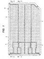
- Fig. 1 is a plan view showing an appearance of a plug-in UICC according to an embodiment of the present invention
- Fig. 2 is a plan view showing an internal structure of the plug-in UICC as seen from a back surface side thereof
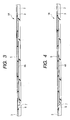
- Fig. 3 is a sectional view of the plug-in UICC taken on line III-III in Fig. 1
- Fig. 4 is a sectional view of the plug-in UICC taken along line IV-IV.
- a body of the plug-in UICC (1A) of this embodiment is constructed of a molding resin 2.
- a tape substrate 3 and a chip 4A mounted on one side of the tape substrate are sealed in the interior of the molding resin 2.
- An opposite side (opposite to the chip mounting side) of the tape substrate 3 is exposed to the exterior of the molding resin 2 and this opposite side constitutes a surface portion of the plug-in UICC (1A).
- Contact patterns 5 as external terminals of the plug-in UICC (1A) are formed on the surface of the tape substrate 3 exposed to the exterior of the molding resin 2.
- An external dimension of the plug-in UICC (1A) is 15 mm long, 25 mm wide and 0.76 mm thick in accordance with ETSI (European Telecommunications Standards Institute).
- One corner of the molding resin 2 which constitutes the body of the plug-in UICC is chamfered for positioning. Each corner is formed with a fillet having a radius of 1 mm. Side faces of the molding resin 2 are tapered at an angle of about 5° to 30°. This taper is formed for carrying out the cutting of the tape substrate 3 as a long tape easily and accurately at the time of cutting the tape substrate with a press into individual pieces or plug-in UICCs (1A) in the final step of the manufacturing process for the plug-in UICC (1A).
- the molding resin 2 is formed of a thermosetting epoxy resin for example. Since the molding resin 2 is high in flexural strength as compared with a potting resin, it is possible to effectively prevent cracking of the chip 4A upon exertion of an external pressure on the plug-in UICC (1A).
- the thickness of the resin (molding resin 2) which seals the chip 4A is large in comparison with the conventional plug-in SIM card with a chip embedded therein. Therefore, even in the case where the size of the chip 4A is large, it is possible to prevent cracking of the chip 4A effectively.
- the chip 4A sealed in the interior of the molding resin 2 is a single crystal silicon chip on which such an integrated circuit as shown in Fig. 2 for example is formed by a known semiconductor device manufacturing process. Its thickness is about 0.1 mm.
- the chip 4A is affixed to one side of the tape substrate 3 with an adhesive.
- the tape substrate 3 comprises a polyimide resin-based insulating film having a thickness of about 0.12 mm and contact patterns 5 formed on the opposite side thereof (opposite to the chip mounting side).
- the contact patterns 5 are formed by etching Cu (copper) foil affixed to the insulating film to form patterns and thereafter plating the pattern surfaces with Ni (nickel) and Au (gold).
- the total thickness of the Cu foil and the plating layer is about 0.04 mm.
- the contact patterns 5 are divided into eight terminals correspondingly to eight contact positions which are indicted with dot-dash lines in Fig. 5.
- One ends of Au wires 7 are connected respectively to the eight terminals through bonding holes 6 formed in the tape substrate 3.
- the eight terminals are electrically connected to bonding pads 8 on the chip 4A through the Au wires 7.
- the bonding holes 6 formed in the tape substrate 3 are arranged in a line near one side of the molding resin 2 so that the chip 4A as a large-size chip can be sealed within the molding resin 2.
- the total area of the contact patterns 5 is larger than the area of the chip 4A and their peripheral edge portions are positioned outside the peripheral edge portions of the chip 4A.
- peripheral edges of the contact patterns 5 are positioned inside the peripheral edges of the molding resin 2, whereby when the tape substrate 3 is pinched between upper and lower die halves of a molding die in a molding step to be described later, there is no fear that the contact patterns 5 may overlap with the upper die half, nor is there any fear that impressions may remain on the surfaces of the contact patterns 5 which would cause a poor appearance.
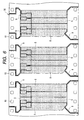
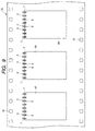
- Fig. 6 is a plan view of a principal portion, showing one side (contact pattern-forming side) of the tape substrate 30 used in fabricating the plug-in UICC (1A) and Fig. 7 is a plan view of a principal portion, showing another side (chip-mounting side) of the tape substrate 30.
- An actual tape substrate 30 is a long tape having a width of 35 mm on which a large number of contact patterns 5 are formed at predetermined intervals.
- Figs. 6 and 7 show an area of three plug-in UICCs (1A).
- power supply lines 9 connected to the contact patterns 5 are formed on both side faces of the tape substrate 30.
- the tape substrate 30 is formed by affixing Cu foil having a thickness of about 0.04 mm to an insulating film having a thickness of about 0.12 mm, then etching the Cu foil to form contact patterns 5 and power supply lines 9 and subsequently plating the surfaces of the contact patterns 5 with Ni and Au while supplying the contact patterns with an electric current through the power supply lines 9.
- the Ni plating layer formed between the Cu foil and the Au plating layer is a barrier layer for preventing interdiffusion of Cu and Au.
- the Ni and Au plating layers may be formed by an electroless plating method instead of an electrolytic plating method. However, the Au plating layer formed by the electrolytic plating method is more lustrous than the Au plating layer formed by the electroless plating layer, so contributes to improving the appearance of the contact patterns 5.
- Sprocket holes 10 for winding and delivering the tape substrate 30 onto and from a reel are formed at predetermined intervals in both side faces of the tape substrate 30.
- the tape substrate 30 is fed to the manufacturing process, then is delivered from the reel and is subjected to various steps (chip mounting step, wire bonding step, molding step, and checking step), then is cut with a press into individual pieces or cards.
- a chip 4A is affixed to one side of the tape substrate 30 with use of an adhesive.
- the total area of the contact patterns 5 is larger than the area of the chip 4A and their peripheral edge portions are positioned outside the peripheral edge portions of the chip 4A. Therefore, a difference in height between the insulating film and the contact patterns 5 does not occur on the adhesive surface of the chip 4A, so that the adhesive surface becomes flat and the strength of bonding between the chip 4A and the tape substrate 30 is improved.
- Au wires 7 are bonded to the contact patterns 5 exposed to the bonding holes 6 in the tape substrate 30 and also to bonding pads 8 on the chip 4A to connect the contact patterns 5 and the chip 4A electrically with each other.
- the tape substrate 30 is loaded into the molding die 12 and is pinched from both sides by an upper die half 12A and a lower die half 12B.
- the peripheral edge portions of the contact patterns 5 formed on the tape substrate 30 are positioned inside end portions of a cavity 12C formed in the upper die half 12A. Therefore, when the tape substrate 30 is loaded into the molding die 12, the contact patterns 5 are not pinched from both sides by the upper and lower die halves 12A, 12B. Thus, there does not occur such an inconvenience that impressions remain on the surfaces of the contact holes 5 by the molding die 12, causing a poor appearance.
- distance L shown in the figure is set at, for example, 0.2 mm or longer, taking a positional deviation between the molding die 12 and the tape substrate 30 into account.
- the molding resin 2 is injected into the cavity 12C through a gate 12D of the molding die 12 to seal the chip 4A.
- plural (six, for example) cavities 12C are formed in the molding die 12 so that plural chips 4A can be sealed at a time.
- Side walls of each cavity 12C are tapered so that a cutting work for the tape substrate 30 can be done easily and accurately in a later pressing step. It is preferable that the angle ( ⁇ ) of the taper be set at, for example, 5° to 30°.
- a groove 12F is formed in the lower die half 12B in each area where power supply lines 9 are formed to prevent the occurrence of a gap between the tape substrate 30 and the upper die half 12A in the vicinity of the power supply lines 9.
- the power supply lines 9 may be drawn out perpendicularly from the contact patterns 5 toward a side of the tape substrate 30.
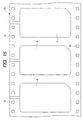
- Fig. 15 is a plan view of a principal portion, showing the tape substrate 30 as removed from the molding die 12 after sealing the chips 4A with the molding resin 2.
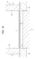
- the tape substrate 30 is cut along the outer periphery of the molding resin 2. This is conducted in the following manner. As shown in Fig. 16, the tape substrate 30 is mounted on a guide 14A of a pressing die 14 and a die 14B is pressed down from above onto the tape substrate 30 to fix the tape substrate, thereafter the tape substrate 30 is cut at positions outside the molding resin 2 with use of a punch 14C to divide the molding resin 2 into individual pieces.
- the plug-in UICC (1A) of this embodiment shown in Figs. 1 to 4 is completed through the steps described above.
- the body of the plug-in UICC (1A) is constructed of the molding resin 2, it is possible to mount a large-sized chip 4A (or plural chips) in comparison with the conventional plug-in SIM card wherein a chip is embedded in a plug-in card, so that it is possible to promote a multi-function structure of the plug-in UICC.
- the assembling work of affixing the tape substrate 30 to the plug-in card becomes unnecessary.
- Fig. 17 is a plan view showing an appearance of a plug-in UICC according to this second embodiment
- Fig. 18 is a plan view showing an internal structure of the plug-in UICC as seen from a back surface side
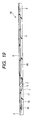
- Fig. 19 is a sectional view of the plug-in UICC.
- the plug-in UICC (1B) of this embodiment is of a construction wherein a chip 4B and an oscillator 15 for USB (Universal Serial Bus) are sealed in the interior of a body constructed of a molding resin 2.
- a tape substrate 3 with the chip 4B and the oscillator 15 for USB mounted thereon there are formed wiring lines 16 connected to the oscillator 15 and also formed electrodes 17.
- the wiring lines 16 and the electrodes 17 are formed by etching Cu foil affixed to one side of an insulating film to form patterns and thereafter plating the surfaces of the patterns with Ni and Au.
- the opposite side of the tape substrate 3 is exposed to the exterior of the molding resin 2 and constitutes a surface portion of the plug-in UICC (1B).
- Contact patterns 5 as external terminals of the plug-in UICC (1B) are formed on the surface of the tape substrate 3 exposed to the exterior of the molding resin 2.
- the contact patterns 5 are formed by etching Cu foil affixed to the opposite side of the insulating film to form patterns and thereafter plating the surfaces of the patterns with Ni and Au.
- Au wires 7 are connected to the contact patterns 5 through bonding holes 6 formed in the tape substrate 3, and the contact patterns 5 are connected electrically to bonding pads 8 on the chip 4B through the Au wires 7.
- the Au wires 7 are connected to both bonding pads 8 on the chip 4B and electrodes 17, and through the Au wires 7 the chip 4B and the oscillator 15 are electrically connected with each other.
- the tape substrate 3 having a wide area can be sealed in the interior of the molding resin 2 by forming the body of the plug-in UICC (1B) with the molding resin, it is possible to implement the plug-in UICC (1B) containing the oscillator 15 for USB which is an electronic part other than the chip 4B.
- Various electronic parts necessary for extending the function of the plug-in UICC (1B) such as, for example, a chip capacitor for RF (Radio Frequency) can be mounted in addition to the oscillator 15 for USB.
- Fig. 20 shows an example in which bonding holes 6 are formed zigzag in the tape substrate 3 so that electrodes 17 are positioned near a chip 4C.
- the tape substrate 3 having a wide area can be sealed in the interior of the molding resin 2, the degree of freedom in the layout of bonding holes 6, wiring lines 16 and electrodes 17 is also improved.
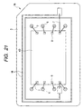
- booster antenna coils 18 may be formed around a chip 4D by etching Cu foil affixed to one side of an insulating film.
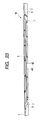
- the molding resin 2 can be made thicker than in the conventional plug-in SIM card wherein a chip is embedded in a plug-in card. Consequently, as shown in Figs. 22 and 23, two chips 4D and 4E can be mounted in a stacked state.
- bonding pads 8 of CPU chip 4E
- bonding pads 8 of FLASH memory chip 4D
- the structures and manufacturing methods as disclosed herein are applicable not only to plug-in UICC but also widely to various plug IC cards, including plug-in SIM card.
- the IC card according to the present invention is suitable for application to a plug-in universal IC card for a portable telephone.
Landscapes
- Engineering & Computer Science (AREA)
- Computer Hardware Design (AREA)
- Microelectronics & Electronic Packaging (AREA)
- Physics & Mathematics (AREA)
- General Physics & Mathematics (AREA)
- Theoretical Computer Science (AREA)
- Credit Cards Or The Like (AREA)
- Encapsulation Of And Coatings For Semiconductor Or Solid State Devices (AREA)
Abstract
Description
Claims (14)
- An IC card, wherein a body of the IC card is comprised of a molding resin, a tape substrate and a semiconductor chip mounted over one side of the tape substrate are sealed in the interior of the molding resin, and external terminals are formed over an opposite side of the tape substrate exposed to the exterior of the molding resin.
- An IC card according to claim 1, wherein back surfaces of the external terminals exposed into a plurality of bonding holes formed over the tape substrate and the semiconductor chip are electrically connected with each other through wires, the plural bonding holes being arranged in a line near one side of the molding resin.
- An IC card according to claim 1 or 2, wherein a total area of the external terminals is larger than the area of the semiconductor chip.
- An IC card according to claim 1, 2 or 3, wherein peripheral edge portions of the external terminals are positioned inside peripheral edge portions of the molding resin.
- An IC card according to claim 4, wherein the peripheral edge portions of the external terminals are positioned 0.2 mm or more inside the peripheral edge portions of the molding resin.
- An IC card according to any one of claims 1 to 5, wherein side walls of the molding resin are tapered.
- An IC card according to any one of claims 1 to 6, wherein an electronic part other than the semiconductor chip is mounted over one side of the tape substrate sealed in the interior of the molding resin.
- An IC card according to any one of claims 1 to 7, wherein a plurality of semiconductor chips are mounted over one side of the tape substrate sealed in the interior of the molding resin.
- An IC card according to claim 8, wherein the plural semiconductor chips are mounted in a stacked state in the height direction of the molding resin.
- An IC card according to any one of claims 1 to 9, wherein peripheral edge portions of the external terminals are positioned outside the peripheral edge portions of the semiconductor chip.
- An IC card according to any one of claims 1 to 10, wherein a total area of the external terminals is smaller than the area of the molding resin.
- A method of manufacturing an IC card, comprising the steps of:(a) providing a tape substrate, the tape substrate having a plurality of chip mounting areas over one side thereof and external terminal patterns formed on opposite sides respectively of the plural chip mounting areas;(b) mounting semiconductor chips respectively over the plural chip mounting areas of the tape substrate;(c) connecting back surfaces of the external terminal patterns exposed into a plurality of bonding holes formed in the tape substrate and the semiconductor chips electrically with each other through wires;(d) loading the tape substrate into a molding die and sealing each of the plural semiconductor chips mounted over the one side of the tape substrate with a molding resin; and(e) cutting the tape substrate along an outer periphery of the molding resin by means of a press to divide the molding resin into individual pieces.
- A method according to claim 12, wherein side walls of a cavity of the molding die are tapered to taper side walls of the molding resin.
- A method according to claim 12 or 13, wherein power supply lines for electrolytically plating surfaces of the external terminal patterns are formed over the opposite side of the tape substrate, a portion of the power supply lines being formed in an area where the power supply lines overlap with air vents of the molding die when the tape substrate is loaded into the molding die.
Applications Claiming Priority (2)
| Application Number | Priority Date | Filing Date | Title |
|---|---|---|---|
| JP2003318099 | 2003-09-10 | ||
| JP2003318099A JP2005085089A (en) | 2003-09-10 | 2003-09-10 | IC card and manufacturing method thereof |
Publications (2)
| Publication Number | Publication Date |
|---|---|
| EP1515269A2 true EP1515269A2 (en) | 2005-03-16 |
| EP1515269A3 EP1515269A3 (en) | 2007-05-16 |
Family
ID=34131994
Family Applications (1)
| Application Number | Title | Priority Date | Filing Date |
|---|---|---|---|
| EP04254322A Withdrawn EP1515269A3 (en) | 2003-09-10 | 2004-07-19 | An integrated circuit card and a method of manufacturing the same |
Country Status (4)
| Country | Link |
|---|---|
| US (1) | US7176060B2 (en) |
| EP (1) | EP1515269A3 (en) |
| JP (1) | JP2005085089A (en) |
| CN (1) | CN1595439A (en) |
Cited By (2)
| Publication number | Priority date | Publication date | Assignee | Title |
|---|---|---|---|---|
| WO2009092547A1 (en) * | 2008-01-21 | 2009-07-30 | Giesecke & Devrient Gmbh | Card-shaped data carrier |
| EP2605188A1 (en) * | 2011-12-14 | 2013-06-19 | Gemalto SA | Method for manufacturing chip cards |
Families Citing this family (19)
| Publication number | Priority date | Publication date | Assignee | Title |
|---|---|---|---|---|
| US8301884B2 (en) | 2002-09-16 | 2012-10-30 | Samsung Electronics Co., Ltd. | Method of managing metadata |
| JP2008504627A (en) * | 2004-06-30 | 2008-02-14 | コーニンクレッカ フィリップス エレクトロニクス エヌ ヴィ | Chip card for holder insertion |
| EP1785916B1 (en) * | 2005-11-14 | 2009-08-19 | Tyco Electronics France SAS | Smartcard body, smart card and method of manufacturing |
| JP4989323B2 (en) * | 2007-06-12 | 2012-08-01 | 株式会社ディスコ | Memory card manufacturing method |
| US8030746B2 (en) * | 2008-02-08 | 2011-10-04 | Infineon Technologies Ag | Integrated circuit package |
| JP5207868B2 (en) * | 2008-02-08 | 2013-06-12 | ルネサスエレクトロニクス株式会社 | Semiconductor device |
| US20090307140A1 (en) | 2008-06-06 | 2009-12-10 | Upendra Mardikar | Mobile device over-the-air (ota) registration and point-of-sale (pos) payment |
| US20140025520A1 (en) * | 2008-06-06 | 2014-01-23 | Ebay Inc. | Biometric authentication of mobile financial transactions by trusted service managers |
| USD686214S1 (en) * | 2011-07-28 | 2013-07-16 | Lifenexus, Inc. | Smartcard with iChip contact pad |
| US8862767B2 (en) | 2011-09-02 | 2014-10-14 | Ebay Inc. | Secure elements broker (SEB) for application communication channel selector optimization |
| US8649820B2 (en) | 2011-11-07 | 2014-02-11 | Blackberry Limited | Universal integrated circuit card apparatus and related methods |
| USD703208S1 (en) | 2012-04-13 | 2014-04-22 | Blackberry Limited | UICC apparatus |
| US8936199B2 (en) | 2012-04-13 | 2015-01-20 | Blackberry Limited | UICC apparatus and related methods |
| USD701864S1 (en) | 2012-04-23 | 2014-04-01 | Blackberry Limited | UICC apparatus |
| JP5952074B2 (en) * | 2012-04-27 | 2016-07-13 | ラピスセミコンダクタ株式会社 | Semiconductor device and measuring instrument |
| JP2014063313A (en) * | 2012-09-20 | 2014-04-10 | Toshiba Corp | Method of manufacturing compact ic card |
| CN108027892B (en) * | 2015-09-18 | 2021-04-09 | X卡控股有限公司 | Self-centering inlays and cores for information carrying cards, processes and resulting products |
| JP6880128B2 (en) * | 2019-09-04 | 2021-06-02 | 三菱電機株式会社 | Electronic equipment unit |
| JP7016200B1 (en) * | 2020-10-30 | 2022-02-04 | 株式会社フェニックスソリューション | Manufacturing method of RFID tag for rubber products and RFID tag for rubber products |
Family Cites Families (16)
| Publication number | Priority date | Publication date | Assignee | Title |
|---|---|---|---|---|
| JP2586831B2 (en) * | 1994-09-22 | 1997-03-05 | 日本電気株式会社 | Resin sealing mold and method of manufacturing semiconductor device |
| US6159770A (en) * | 1995-11-08 | 2000-12-12 | Fujitsu Limited | Method and apparatus for fabricating semiconductor device |
| US6171888B1 (en) * | 1996-03-08 | 2001-01-09 | Lsi Logic Corp. | Multi-layer tab tape having distinct signal, power and ground planes, semiconductor device assembly employing same, apparatus for and method of assembling same |
| JP3572833B2 (en) * | 1996-12-19 | 2004-10-06 | 株式会社デンソー | Method for manufacturing resin-encapsulated semiconductor device |
| US6177288B1 (en) * | 1998-06-19 | 2001-01-23 | National Semiconductor Corporation | Method of making integrated circuit packages |
| JP2000012745A (en) * | 1998-06-24 | 2000-01-14 | Nec Corp | Semiconductor package and manufacturing method thereof |
| US6404643B1 (en) * | 1998-10-15 | 2002-06-11 | Amerasia International Technology, Inc. | Article having an embedded electronic device, and method of making same |
| FR2797977B1 (en) * | 1999-08-25 | 2004-09-24 | Gemplus Card Int | MANUFACTURING PROCESS OF A PORTABLE ELECTRONIC DEVICE INCLUDING AN OVERMOLDING STEP DIRECTLY ON THE SUPPORT FILM |
| JP3768761B2 (en) * | 2000-01-31 | 2006-04-19 | 株式会社日立製作所 | Semiconductor device and manufacturing method thereof |
| JP2001274316A (en) * | 2000-03-23 | 2001-10-05 | Hitachi Ltd | Semiconductor device and manufacturing method thereof |
| WO2001084490A1 (en) * | 2000-04-28 | 2001-11-08 | Hitachi,Ltd | Ic card |
| JP2001344583A (en) | 2000-06-01 | 2001-12-14 | Dainippon Printing Co Ltd | IC carrier |
| US6824063B1 (en) | 2000-08-04 | 2004-11-30 | Sandisk Corporation | Use of small electronic circuit cards with different interfaces in an electronic system |
| JP2003086750A (en) * | 2001-09-11 | 2003-03-20 | Rohm Co Ltd | Manufacturing method of electronic components |
| US6965160B2 (en) * | 2002-08-15 | 2005-11-15 | Micron Technology, Inc. | Semiconductor dice packages employing at least one redistribution layer |
| JP4159431B2 (en) * | 2002-11-15 | 2008-10-01 | 株式会社ルネサステクノロジ | Manufacturing method of semiconductor device |
-
2003
- 2003-09-10 JP JP2003318099A patent/JP2005085089A/en active Pending
-
2004
- 2004-07-19 EP EP04254322A patent/EP1515269A3/en not_active Withdrawn
- 2004-07-29 CN CNA2004100703215A patent/CN1595439A/en active Pending
- 2004-07-30 US US10/902,024 patent/US7176060B2/en not_active Expired - Fee Related
Cited By (5)
| Publication number | Priority date | Publication date | Assignee | Title |
|---|---|---|---|---|
| WO2009092547A1 (en) * | 2008-01-21 | 2009-07-30 | Giesecke & Devrient Gmbh | Card-shaped data carrier |
| US8960556B2 (en) | 2008-01-21 | 2015-02-24 | Giesecke & Devrient Gmbh | Card-shaped data carrier |
| EP2605188A1 (en) * | 2011-12-14 | 2013-06-19 | Gemalto SA | Method for manufacturing chip cards |
| WO2013087541A1 (en) * | 2011-12-14 | 2013-06-20 | Gemalto S.A. | Method for manufacturing smart cards |
| US9165236B2 (en) | 2011-12-14 | 2015-10-20 | Gemalto Sa | Method for manufacturing smart cards |
Also Published As
| Publication number | Publication date |
|---|---|
| CN1595439A (en) | 2005-03-16 |
| US20050052851A1 (en) | 2005-03-10 |
| EP1515269A3 (en) | 2007-05-16 |
| US7176060B2 (en) | 2007-02-13 |
| JP2005085089A (en) | 2005-03-31 |
Similar Documents
| Publication | Publication Date | Title |
|---|---|---|
| US7176060B2 (en) | Integrated circuit card and a method of manufacturing the same | |
| KR0139700B1 (en) | Semiconductor device, lead frame and a method for manufacturing the semiconductor device | |
| US6730995B2 (en) | Two-stage transfer molding device to encapsulate MMC module | |
| US6861734B2 (en) | Resin-molded semiconductor device | |
| CN1143383C (en) | Chip method especially for implantation in chip card body | |
| CN1167039C (en) | IC module and IC card with IC module | |
| US7193161B1 (en) | SiP module with a single sided lid | |
| KR100283299B1 (en) | Plastic-encapsulated semiconductor device and fabrication method thereof | |
| US20050110127A1 (en) | Semiconductor device | |
| US6617200B2 (en) | System and method for fabricating a semiconductor device | |
| KR100274854B1 (en) | Lead frame for semiconductor device and semiconductor device | |
| JP2001035961A (en) | Semiconductor device and manufacturing method thereof | |
| JP2981194B2 (en) | Semiconductor chip package | |
| JP4961636B2 (en) | Non-contact type IC card and manufacturing method thereof | |
| JPH11354689A (en) | Frame-shaped substrate, method of manufacturing the same, and method of manufacturing a semiconductor device | |
| JP4522802B2 (en) | IC module | |
| KR100537893B1 (en) | Leadframe and multichip package using the same | |
| KR0145767B1 (en) | Thin film semiconductor package and the manufacturing method | |
| JP2001143039A (en) | Semiconductor device and manufacturing method thereof | |
| JP2001168123A (en) | Semiconductor device and manufacturing method thereof, semiconductor device manufacturing apparatus, circuit board, and electronic equipment | |
| JP2008097073A (en) | IC card module, manufacturing method thereof and IC card | |
| KR20060025118A (en) | Manufacturing method of metal base equipment and IC card module | |
| JP2003187206A (en) | Semiconductor device and manufacturing method thereof | |
| JP2000049178A (en) | Semiconductor device and manufacturing method thereof | |
| JPH08111490A (en) | Semiconductor device, manufacturing method thereof, and lead frame used for the same |
Legal Events
| Date | Code | Title | Description |
|---|---|---|---|
| PUAI | Public reference made under article 153(3) epc to a published international application that has entered the european phase |
Free format text: ORIGINAL CODE: 0009012 |
|
| 17P | Request for examination filed |
Effective date: 20040809 |
|
| AK | Designated contracting states |
Kind code of ref document: A2 Designated state(s): AT BE BG CH CY CZ DE DK EE ES FI FR GB GR HU IE IT LI LU MC NL PL PT RO SE SI SK TR |
|
| AX | Request for extension of the european patent |
Extension state: AL HR LT LV MK |
|
| PUAL | Search report despatched |
Free format text: ORIGINAL CODE: 0009013 |
|
| AK | Designated contracting states |
Kind code of ref document: A3 Designated state(s): AT BE BG CH CY CZ DE DK EE ES FI FR GB GR HU IE IT LI LU MC NL PL PT RO SE SI SK TR |
|
| AX | Request for extension of the european patent |
Extension state: AL HR LT LV MK |
|
| AKX | Designation fees paid |
Designated state(s): DE FR GB IT NL |
|
| STAA | Information on the status of an ep patent application or granted ep patent |
Free format text: STATUS: THE APPLICATION IS DEEMED TO BE WITHDRAWN |
|
| 18D | Application deemed to be withdrawn |
Effective date: 20100202 |