EP1514274B1 - Memory storage device with heating element - Google Patents
Memory storage device with heating element Download PDFInfo
- Publication number
- EP1514274B1 EP1514274B1 EP02807323A EP02807323A EP1514274B1 EP 1514274 B1 EP1514274 B1 EP 1514274B1 EP 02807323 A EP02807323 A EP 02807323A EP 02807323 A EP02807323 A EP 02807323A EP 1514274 B1 EP1514274 B1 EP 1514274B1
- Authority
- EP
- European Patent Office
- Prior art keywords
- storage device
- cell
- memory storage
- storage cell
- magnetic region
- Prior art date
- Legal status (The legal status is an assumption and is not a legal conclusion. Google has not performed a legal analysis and makes no representation as to the accuracy of the status listed.)
- Expired - Lifetime
Links
- 238000010438 heat treatment Methods 0.000 title claims abstract description 30
- 230000005055 memory storage Effects 0.000 title claims abstract description 26
- 210000000352 storage cell Anatomy 0.000 claims abstract description 62
- 230000005291 magnetic effect Effects 0.000 claims abstract description 60
- 230000005415 magnetization Effects 0.000 claims abstract description 43
- 230000008859 change Effects 0.000 claims abstract description 11
- 239000000463 material Substances 0.000 claims abstract description 11
- 210000004027 cell Anatomy 0.000 claims description 40
- 230000002441 reversible effect Effects 0.000 claims description 13
- 239000002902 ferrimagnetic material Substances 0.000 claims description 8
- 230000000063 preceeding effect Effects 0.000 claims 1
- 238000004519 manufacturing process Methods 0.000 abstract description 3
- 241001581440 Astroides Species 0.000 description 7
- 230000005641 tunneling Effects 0.000 description 6
- 238000000034 method Methods 0.000 description 5
- 238000003491 array Methods 0.000 description 4
- 238000013500 data storage Methods 0.000 description 4
- 230000006870 function Effects 0.000 description 4
- 230000008569 process Effects 0.000 description 4
- 229910045601 alloy Inorganic materials 0.000 description 3
- 239000000956 alloy Substances 0.000 description 3
- 230000004888 barrier function Effects 0.000 description 3
- XUIMIQQOPSSXEZ-UHFFFAOYSA-N Silicon Chemical compound [Si] XUIMIQQOPSSXEZ-UHFFFAOYSA-N 0.000 description 2
- 230000007123 defense Effects 0.000 description 2
- 230000035945 sensitivity Effects 0.000 description 2
- 229910052710 silicon Inorganic materials 0.000 description 2
- 239000010703 silicon Substances 0.000 description 2
- 239000000758 substrate Substances 0.000 description 2
- RYGMFSIKBFXOCR-UHFFFAOYSA-N Copper Chemical compound [Cu] RYGMFSIKBFXOCR-UHFFFAOYSA-N 0.000 description 1
- 229910052692 Dysprosium Inorganic materials 0.000 description 1
- 229910052688 Gadolinium Inorganic materials 0.000 description 1
- 229910052772 Samarium Inorganic materials 0.000 description 1
- 229910052771 Terbium Inorganic materials 0.000 description 1
- 229910052782 aluminium Inorganic materials 0.000 description 1
- XAGFODPZIPBFFR-UHFFFAOYSA-N aluminium Chemical compound [Al] XAGFODPZIPBFFR-UHFFFAOYSA-N 0.000 description 1
- PNEYBMLMFCGWSK-UHFFFAOYSA-N aluminium oxide Inorganic materials [O-2].[O-2].[O-2].[Al+3].[Al+3] PNEYBMLMFCGWSK-UHFFFAOYSA-N 0.000 description 1
- 230000006399 behavior Effects 0.000 description 1
- 229910052802 copper Inorganic materials 0.000 description 1
- 239000010949 copper Substances 0.000 description 1
- 229910052593 corundum Inorganic materials 0.000 description 1
- 230000008878 coupling Effects 0.000 description 1
- 238000010168 coupling process Methods 0.000 description 1
- 238000005859 coupling reaction Methods 0.000 description 1
- 230000003247 decreasing effect Effects 0.000 description 1
- 238000013461 design Methods 0.000 description 1
- 238000009792 diffusion process Methods 0.000 description 1
- 230000000694 effects Effects 0.000 description 1
- 238000005516 engineering process Methods 0.000 description 1
- 238000002474 experimental method Methods 0.000 description 1
- 230000005308 ferrimagnetism Effects 0.000 description 1
- 238000002347 injection Methods 0.000 description 1
- 239000007924 injection Substances 0.000 description 1
- 229910052742 iron Inorganic materials 0.000 description 1
- 230000007246 mechanism Effects 0.000 description 1
- 229910052751 metal Inorganic materials 0.000 description 1
- 239000002184 metal Substances 0.000 description 1
- 238000012986 modification Methods 0.000 description 1
- 230000004048 modification Effects 0.000 description 1
- 239000002245 particle Substances 0.000 description 1
- 230000000704 physical effect Effects 0.000 description 1
- 229910052761 rare earth metal Inorganic materials 0.000 description 1
- 150000002910 rare earth metals Chemical class 0.000 description 1
- 238000011160 research Methods 0.000 description 1
- WFKWXMTUELFFGS-UHFFFAOYSA-N tungsten Chemical compound [W] WFKWXMTUELFFGS-UHFFFAOYSA-N 0.000 description 1
- 229910052721 tungsten Inorganic materials 0.000 description 1
- 239000010937 tungsten Substances 0.000 description 1
- 229910001845 yogo sapphire Inorganic materials 0.000 description 1
Images



Classifications
-
- G—PHYSICS
- G11—INFORMATION STORAGE
- G11C—STATIC STORES
- G11C11/00—Digital stores characterised by the use of particular electric or magnetic storage elements; Storage elements therefor
- G11C11/02—Digital stores characterised by the use of particular electric or magnetic storage elements; Storage elements therefor using magnetic elements
- G11C11/14—Digital stores characterised by the use of particular electric or magnetic storage elements; Storage elements therefor using magnetic elements using thin-film elements
- G11C11/15—Digital stores characterised by the use of particular electric or magnetic storage elements; Storage elements therefor using magnetic elements using thin-film elements using multiple magnetic layers
-
- G—PHYSICS
- G11—INFORMATION STORAGE
- G11C—STATIC STORES
- G11C11/00—Digital stores characterised by the use of particular electric or magnetic storage elements; Storage elements therefor
- G11C11/02—Digital stores characterised by the use of particular electric or magnetic storage elements; Storage elements therefor using magnetic elements
- G11C11/16—Digital stores characterised by the use of particular electric or magnetic storage elements; Storage elements therefor using magnetic elements using elements in which the storage effect is based on magnetic spin effect
-
- G—PHYSICS
- G11—INFORMATION STORAGE
- G11C—STATIC STORES
- G11C11/00—Digital stores characterised by the use of particular electric or magnetic storage elements; Storage elements therefor
- G11C11/02—Digital stores characterised by the use of particular electric or magnetic storage elements; Storage elements therefor using magnetic elements
- G11C11/16—Digital stores characterised by the use of particular electric or magnetic storage elements; Storage elements therefor using magnetic elements using elements in which the storage effect is based on magnetic spin effect
- G11C11/165—Auxiliary circuits
- G11C11/1675—Writing or programming circuits or methods
-
- G—PHYSICS
- G11—INFORMATION STORAGE
- G11C—STATIC STORES
- G11C11/00—Digital stores characterised by the use of particular electric or magnetic storage elements; Storage elements therefor
- G11C11/18—Digital stores characterised by the use of particular electric or magnetic storage elements; Storage elements therefor using Hall-effect devices
-
- G—PHYSICS
- G11—INFORMATION STORAGE
- G11C—STATIC STORES
- G11C7/00—Arrangements for writing information into, or reading information out from, a digital store
- G11C7/02—Arrangements for writing information into, or reading information out from, a digital store with means for avoiding parasitic signals
-
- G—PHYSICS
- G11—INFORMATION STORAGE
- G11C—STATIC STORES
- G11C7/00—Arrangements for writing information into, or reading information out from, a digital store
- G11C7/04—Arrangements for writing information into, or reading information out from, a digital store with means for avoiding disturbances due to temperature effects
-
- H—ELECTRICITY
- H10—SEMICONDUCTOR DEVICES; ELECTRIC SOLID-STATE DEVICES NOT OTHERWISE PROVIDED FOR
- H10B—ELECTRONIC MEMORY DEVICES
- H10B61/00—Magnetic memory devices, e.g. magnetoresistive RAM [MRAM] devices
-
- H—ELECTRICITY
- H10—SEMICONDUCTOR DEVICES; ELECTRIC SOLID-STATE DEVICES NOT OTHERWISE PROVIDED FOR
- H10N—ELECTRIC SOLID-STATE DEVICES NOT OTHERWISE PROVIDED FOR
- H10N50/00—Galvanomagnetic devices
- H10N50/80—Constructional details
- H10N50/85—Materials of the active region
Definitions
- the present invention generally relates to memory arrays of storage cells, and more particularly to a memory storage device with a heating element.
- Magnetic Random Access Memory (MRAM) technology utilizes storage cells, for example, magnetic tunnel junctions (MTJs), which generally each have at least two magnetic regions or layers with an electrically insulating barrier layer between them.
- the data storage mechanism relies on the relative orientation of the magnetization of the two layers, and on the ability to discern this orientation through electrodes attached to these layers.
- MTJs magnetic tunnel junctions
- the data storage mechanism relies on the relative orientation of the magnetization of the two layers, and on the ability to discern this orientation through electrodes attached to these layers.
- each storage cell includes a magnetically changeable (reversible) or "free” region and a proximate magnetically referenced “fixed” region arranged into a MTJ.
- a storage cell can be written by reversing the free region magnetization using applied bi-directional electrical and resultant magnetic stimuli via its respective bit line and word line.
- the storage cell can later be read by measuring the resultant tunneling resistance between the bit line and word line, which assumes one of two values depending on the relative orientation of the magnetization of the free region with respect to the fixed region.
- MRAM arrays typically include an array of data storage cells respectively positioned at intersections of word lines and bit lines.
- the magnetic fields generated from the bit and word line during writing can disturb the magnetization state of adjacent non-selected cells, thereby reducing reliability of the array.
- the magnetic state of a cell can be affected by the magnetization state of adjacent cells, especially in a dense array.
- the present invention accordingly provides, in a first aspect, a memory storage device according to claim 1.
- the changeable magnetic region is a reversible magnetic region having a magnetization state which can be reversed by applying thereto a selected magnetic field, said reversible magnetic region comprising a material having a magnetization state that is responsive to a change in the temperature thereof.
- the storage cell further comprises at least one fixed magnetic region having a magnetization state which does not reverse when said selected magnetic field is applied thereto.
- the material having a magnetization state that is responsive to a change in temperature thereof comprises a ferrimagnetic material.
- the changeable magnetic region is maintained at a compensation temperature of said material to maintain stored data in said storage cell.
- the present invention further provides, in a second aspect, an integrated circuit comprising at least one memory storage device as described above.
- MRAM arrays include an array of data storage cells 50 typically positioned at the intersections of wordlines 1, 2, 3 and bitlines 4, 5, 6, as shown in FIG. 1 .
- each cell includes a magnetically changeable (reversible) or “free” region, and a proximate, magnetically referenced or “fixed” region, arranged into a MTJ device.
- the term "fixed region” is used broadly herein to denote any type of region which, in cooperation with the free or changeable region, results in a detectable state of the device as a whole.
- the principle underlying storage of data in such cells is the ability to change, and even reverse, the relative orientation of the magnetization of the free regions with respect to the corresponding fixed regions by changing the direction of magnetization along the easy axis ("EA") of the free region, and the ability to thereafter read this relative orientation difference. More particularly, a storage cell is written by reversing the free region magnetization using applied bi-directional electrical and resultant magnetic stimuli via its respective bit line and word line.
- the storage cell is later read by measuring the resultant tunneling resistance between the bit line and word line, which assumes one of two values depending on the relative orientation of the magnetization of the free region with respect to the fixed region. If the free region is modeled as a simple elemental magnet having a direction of magnetization which is free to rotate but with a strong preference for aligning in either direction along its easy axis (+EA or -EA), and if the reference region is a similar elemental magnet but having a direction of magnetization fixed in the +EA direction, then two states, and therefore two possible tunneling resistance values, are defined for the cell: aligned or parallel (+EA/+EA) and anti-aligned or anti-parallel (-EA/+EA).
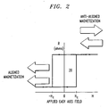
- FIG. 2 An ideal hysteresis loop characterizing the tunnel junction resistance with respect to the applied EA field is shown in FIG. 2 .
- the resistance of the tunnel junction can assume one of two distinct values with no applied stimulus in region 20, i.e., there is a lack of sensitivity of resistance to the applied field below the easy axis flipping field strength +/- H c in region 20.
- the storage cell can be read by measuring the tunneling resistance to infer the magnetization state of the free layer with respect to the fixed layer.
- the ideal hysteresis loop shown schematically in FIG. 2 , is desirable since the resistance has one of two distinct possibilities, and there is a lack of sensitivity of measured resistance to the applied field below the flipping field strength H c .
- H c flipping field strength
- FIGS. 3(a) and 3(b) illustrate a geometry typically proposed for addressing the storage cell 50.
- the bias current indicated by the arrow through the cell 50 flows from bit line 5 to word line 2, as shown in FIG. 3(a) , while the magnetic field-generating current flows in either bit line 5 or word line 2 as indicated by the arrows as shown in FIG. 3(b) .
- FIG. 4 graphically illustrates the magnetic selectivity of an ideal magnetic memory cell (a so-called "astroid plot” or Stoner-Wolfarth astroid) and selective switching of cells in an array.
- the solid line 40 traces the boundaries of stability for a single idealized particle for magnetization pointing either left or right as a function of applied magnetic field.
- the axes of the plot correspond to the easy (H casy ) and hard (H hard ) axis fields (i.e., parallel or perpendicular to the direction preferred by the crystalline anisotropy).
- the magnetic field may be used to isolate a particular data storage cell for writing.
- the solid line 40 of the astroid curve expands into a band when considering the range of stability for a population of junctions. If this band becomes too large, then there is no combination of easy and hard axis fields which will definitely switch any desired storage cell, without also switching other unselected storage cells by mistake. Thus, reliability becomes a problem.
- the magnetic field at a storage cell is affected by not only the fields from the bit and word lines, but also to the magnetic state of the storage cells around it. This effect, when considered statistically, further reduces write selectivity.
- the preferred embodiment of the present invention provides a memory array utilizing a memory storage device design in which a write selectivity of a storage cell, e.g., a MTJ, or group of storage cells may be selectively increased by heating only the selected cell(s), thereby reducing the likelihood of unintentionally writing adjacent cells, and improving the quality of the switching characteristics of the selected cell(s).
- a write selectivity of a storage cell e.g., a MTJ, or group of storage cells
- an exemplary memory array includes a set of electrically conductive lines that function as parallel word lines 1, 2, and 3 in a horizontal plane, and a set of electrically conductive lines that function as parallel bit lines 4, 5, and 6 in another horizontal plane.
- the bit lines are preferably oriented in a different direction, e.g., at right angles to the word lines, so that the two sets of lines form intersecting regions when viewed from above.
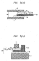
- a storage cell 50 for example, a MTJ device, which is shown in greater detail in FIGS. 5(a) and 5(b) with regard to the present invention, is located at a plurality of intersecting regions of a word line and a bit line, vertically spaced between the lines. Three word lines and three bit lines are illustrated in FIG. 1 , but the number of lines would typically be much larger.
- Storage cell 50 e.g., a MTJ device
- storage cell 50 is preferably formed of a number of vertically stacked regions or layers.
- cell 50 comprises both a fixed layer 52 and a changeable or "free" layer 51 separated by an electrically insulating tunnel barrier layer 53.
- the magnetization of fixed layer 52 is oriented in the plane of the layer but is fixed so that it may not be rotated or reversed in the presence of applied external magnetic fields generated by write currents through bit line 5 and word line 2.
- the magnetization of free layer 51 can be rotated (or reversed) in the plane of layer 51 relative to the fixed magnetization of layer 52.
- the amount of tunneling current that flows perpendicularly through magnetic layers 51 and 52 and through the intermediate tunneling insulating layer 53, e.g., Al 2 O 3 depends on the relative magnetization directions of magnetic layers 51 and 52.
- the free layer 51 is fabricated to have a preferred axis for the direction of magnetization called the easy axis. There are two possible stable reversible directions of magnetization of the free layer 51 along this easy axis which define two stable states of the storage cell 50.
- the cell 50 can be written by changing the magnetization of the free layer 51.
- the magnetization of the free layer can be changed, for example, when a sufficiently large current is passed through both a word line 2 and a bit line 5 of the storage cell 50.
- the field generated by the combined magnetic fields at the intersection of the word and bit lines will rotate the magnetization of the free layer 51 of the single particular cell 50 located at the intersection of the energized word and bit lines.
- the field generated by current passing through a single word or bit line alone may be sufficient to rotate the magnetization of the free layer 51 of the cell 50 when the cell 50 is selected as further described below.
- the current levels are designed so that the field produced exceeds the switching field of the free layer 51.
- the storage cell 50 is designed so that the field required to switch the magnetization of the fixed layer 52 is much greater than the field required to switch the free layer 51.
- Another example of changing the magnetization of the free layer is via spin injection, wherein the spin state of the electrons of current passing through the cell operatively affects the magnetization of the free layer.
- the state of the storage cell 50 may be determined, for example, by measuring the resistance of the storage cell 50 when a read current, much smaller than the write current, is passed perpendicularly through the cell.
- the field generated by this read current is preferably negligible and therefore does not switch the magnetic state of storage cell 50.
- the magnetic field required to switch that specific cell can be reduced. If the magnetic field is applied simultaneously, or at least before the layer 51 recools, only the heated cell will be written, provided that the magnetic field strength is both larger than the coercivity of the heated cell and smaller than the coercivity of the unheated cell.
- the present invention provides a memory storage device 58 that removes the heating function from the storage cell 50, thereby removing constraints on the choice of storage cells, e.g., tunnel barriers having a certain range of resistance.
- the memory storage device of the invention can remove possible limits on the available densities of the memory array.
- the memory storage device 58 of the invention includes a heating element 56 and a storage cell 50 as described above.
- the heating element 56 is separate from the storage cell 50 and preferably comprises a conductive layer having a low resistance, e.g., from about 1 to about 100 ohms, in order to permit sufficient heat to be generated by a given electric current passing through the heating element 56.
- Suitable materials for forming the heating element layer 56 include, for example, tungsten, copper, aluminum, and doped silicon.
- the heating element 56 is heated by an external energy source (not shown).
- the energy source can be, for example, a voltage or current source, or a heat source. As shown in FIGS. 5(a) and 5(b) , electric current can pass through the word line 2 into the heating element 56. Although other configurations are possible, it is preferred that the heating element 56 be heated by current passing from an adjacent word line.
- the memory storage device 58 of the invention also includes an output terminal 54.
- the output terminal 54 can be formed of any conventional material, such as metal, suitable for carrying current. It is preferred that the conductive terminal 54 not be magnetic.
- the output terminal 54 can accept current passing through the heating element 56 and serve as a return to an external voltage or current source that provided the current.
- FIGS. 5(a) and 5(b) show two preferred arrangements of the elements within the memory device 58, and the coupling of the memory device 58 to the word lines 2 and bit lines 5 in a memory array.
- the heating element 56 is adjacent to the word line 2.
- the word and bit lines could be reversed.
- the heating element 56 should be proximate to the storage cell 50 such that the heat from the heating element 56 can be substantially localized to the selected storage cell 50, thereby raising the temperature of the storage cell 50 without also heating adjacent storage cells.
- the coercive field is reduced in the storage cell 50. Therefore, a much smaller magnetic field can be applied to reverse the direction of magnetization in the free layer 51. In contrast, during the read process, a smaller current is typically used, whereby the reading operation leaves the stored magnetization state intact.
- thermally assisted switching ensures that when the cell is not activated (e.g., heated), the cold-state coercivity is comparatively large and thus unintentional switching is minimized.
- the free layer 51 of storage cell 50 includes ferrimagnetic material.
- ferrimagnetic materials often include a plurality (e.g., two) of sub-lattices with opposing magnetization.
- the two sub-lattices in a ferrimagnet are not identical, the physical properties of a ferrimagnet are quite different from those of an anti-ferromagnet.
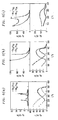
- Ferrimagnetism is usually observed in rare earth alloys such as those indicated in FIGS. 6 (a)-(c) .
- ferrimagnetic materials include alloys of Fe and at least one of Gd, Tb, and Dy, e.g., Gd 23 Fe 77 , Gd 24 Fe 76 , Tb 19 Fe 81 , Tb 21 Fe 79 , Dy 17 Fe 83 , and Dy 21 Fe 79 .
- Other examples of ferrimagnetic materials include alloys of Co and Sm.
- the moments of the two sub-lattices of ferrimagnetic materials are unequal so that there is a net macroscopic moment.
- the magnetizations of the sub-lattices have different temperature dependence so that there can be a temperature at which they exactly compensate for one another.
- T comp compensation temperature
- the coercivity is very high as there is no net moment to be rotated by an externally applied magnetic field.
- Small changes in temperature close to the compensation point can lead to dramatic changes in coercivity, as shown in FIGS. 6(a)-6(c) .
- changes of as little as about 5 °C to about 10°C can provide an order of magnitude change in the coercive external magnetic field.
- temperature control may be provided for the storage cell to more precisely define the hot and cold coercive fields, using, for example, the guidance of graphs such as those shown in FIGS. 6(a)-6(c) .
- the guidance of graphs such as those shown in FIGS. 6(a)-6(c) .
- the speed of the thermal selection process is also expected to be quite rapid.
- other experiments on small geometries e.g., see Williams et al., "Scanning Thermal Profiler," Appl. Phys. Lett. 23, pp. 1587-1589 ) have shown thermal time constants in some cases to be shorter than 1 nanosecond (ns).
- ns nanosecond
- the lateral diffusion time constant for heat to propagate in metallic films would be on the order of 1 ns.
- the selection process of heating a junction need not be the rate-limiting element in an MRAM array.
- an integrated circuit is provided.
- the memory storage device 58 of the memory array may be formed on a substrate, such as a silicon substrate on which there may be included other circuitry to form an integrated circuit.
- the integrated circuit of the invention includes a memory storage device as described above.
Landscapes
- Engineering & Computer Science (AREA)
- Computer Hardware Design (AREA)
- Mram Or Spin Memory Techniques (AREA)
- Semiconductor Memories (AREA)
- Hall/Mr Elements (AREA)
- Surface Heating Bodies (AREA)
- Fixed Capacitors And Capacitor Manufacturing Machines (AREA)
- Oscillators With Electromechanical Resonators (AREA)
Abstract
Description
- This invention was made with Government support under grant contract numbers MDA972-96-C-Z0030 and MDA972-99-C-0009 awarded by the Defense Advanced Research Projects Agency (DARPA) of the United States Department of Defense. The Government has certain rights in this invention.
- The present invention generally relates to memory arrays of storage cells, and more particularly to a memory storage device with a heating element.
- Magnetic Random Access Memory (MRAM) technology utilizes storage cells, for example, magnetic tunnel junctions (MTJs), which generally each have at least two magnetic regions or layers with an electrically insulating barrier layer between them. The data storage mechanism relies on the relative orientation of the magnetization of the two layers, and on the ability to discern this orientation through electrodes attached to these layers. For background, reference is made to United States Patent Nos.
5,650,958 and5,640,343 issued to Gallagher et al. on July 22, 1997 and June 17, 1997, respectively. - Typically, each storage cell includes a magnetically changeable (reversible) or "free" region and a proximate magnetically referenced "fixed" region arranged into a MTJ. A storage cell can be written by reversing the free region magnetization using applied bi-directional electrical and resultant magnetic stimuli via its respective bit line and word line. The storage cell can later be read by measuring the resultant tunneling resistance between the bit line and word line, which assumes one of two values depending on the relative orientation of the magnetization of the free region with respect to the fixed region.
- MRAM arrays typically include an array of data storage cells respectively positioned at intersections of word lines and bit lines. When writing storage cells, it is desirable to write only selected storage cells in the array, without affecting other non-selected cells. However, the magnetic fields generated from the bit and word line during writing can disturb the magnetization state of adjacent non-selected cells, thereby reducing reliability of the array. In addition, the magnetic state of a cell can be affected by the magnetization state of adjacent cells, especially in a dense array.
- Accordingly, a need exists for improving the write selectivity of memory storage cells within a memory array.
- International patent application publication number
WO 00/79540 (Daughton et al - The present invention accordingly provides, in a first aspect, a memory storage device according to claim 1.
- Preferably, the changeable magnetic region is a reversible magnetic region having a magnetization state which can be reversed by applying thereto a selected magnetic field, said reversible magnetic region comprising a material having a magnetization state that is responsive to a change in the temperature thereof.
- Preferably, the storage cell further comprises at least one fixed magnetic region having a magnetization state which does not reverse when said selected magnetic field is applied thereto.
- Preferably, the material having a magnetization state that is responsive to a change in temperature thereof comprises a ferrimagnetic material.
- Preferably, the changeable magnetic region is maintained at a compensation temperature of said material to maintain stored data in said storage cell.
- The present invention further provides, in a second aspect, an integrated circuit comprising at least one memory storage device as described above.
-
-
FIG. 1 schematically illustrates a magnetic memory array of MRAM magnetic storage cells suitable for use with the present invention; -
FIG. 2 schematically illustrates an ideal hysteresis loop for a reversible magnetic region of a MRAM storage cell; -
FIGS. 3(a) and 3(b) schematically illustrate a geometry for addressing a MRAM storage cell; -
FIG. 4 graphically illustrates the magnetic selectivity of an ideal magnetic memory cell for selectively switching the magnetic state of the memory; -
FIG. 5(a) schematically illustrates a memory storage device, formed in accordance with one aspect of the present invention; -
FIG. 5(b) schematically illustrates a memory storage device, formed in accordance with another aspect of the present invention; -
FIGS. 6(a)-6(c) schematically illustrate the temperature dependence of the coercive field of selected ferrimagnetic materials suitable for use in the magnetic tunnel junction, according to the present invention. - MRAM arrays include an array of
data storage cells 50 typically positioned at the intersections ofwordlines bitlines FIG. 1 . In a preferred form, each cell includes a magnetically changeable (reversible) or "free" region, and a proximate, magnetically referenced or "fixed" region, arranged into a MTJ device. The term "fixed region" is used broadly herein to denote any type of region which, in cooperation with the free or changeable region, results in a detectable state of the device as a whole. - Generally, the principle underlying storage of data in such cells is the ability to change, and even reverse, the relative orientation of the magnetization of the free regions with respect to the corresponding fixed regions by changing the direction of magnetization along the easy axis ("EA") of the free region, and the ability to thereafter read this relative orientation difference. More particularly, a storage cell is written by reversing the free region magnetization using applied bi-directional electrical and resultant magnetic stimuli via its respective bit line and word line.
- The storage cell is later read by measuring the resultant tunneling resistance between the bit line and word line, which assumes one of two values depending on the relative orientation of the magnetization of the free region with respect to the fixed region. If the free region is modeled as a simple elemental magnet having a direction of magnetization which is free to rotate but with a strong preference for aligning in either direction along its easy axis (+EA or -EA), and if the reference region is a similar elemental magnet but having a direction of magnetization fixed in the +EA direction, then two states, and therefore two possible tunneling resistance values, are defined for the cell: aligned or parallel (+EA/+EA) and anti-aligned or anti-parallel (-EA/+EA).
- An ideal hysteresis loop characterizing the tunnel junction resistance with respect to the applied EA field is shown in
FIG. 2 . The resistance of the tunnel junction can assume one of two distinct values with no applied stimulus inregion 20, i.e., there is a lack of sensitivity of resistance to the applied field below the easy axis flipping field strength +/- Hc inregion 20. - For example, if the applied easy axis field exceeds +/-Hc, then the cell is coerced into its respective high resistance (anti-aligned magnetization of the free region with respect to the fixed region) or low resistance (aligned magnetization of the free region with respect to the fixed region) state. Thus, in operation as a memory device, the storage cell can be read by measuring the tunneling resistance to infer the magnetization state of the free layer with respect to the fixed layer.
- The ideal hysteresis loop, shown schematically in
FIG. 2 , is desirable since the resistance has one of two distinct possibilities, and there is a lack of sensitivity of measured resistance to the applied field below the flipping field strength Hc. However, in a practical device, such ideal behavior often fails to exist, thereby raising many problems. -
FIGS. 3(a) and 3(b) illustrate a geometry typically proposed for addressing thestorage cell 50. The bias current indicated by the arrow through thecell 50 flows frombit line 5 toword line 2, as shown inFIG. 3(a) , while the magnetic field-generating current flows in eitherbit line 5 orword line 2 as indicated by the arrows as shown inFIG. 3(b) . - Although the ability to cleanly write the bit (corresponding to the reversal of the free layer in the storage cell geometry discussed above) is important, there is another important aspect for the successful operation of the MRAM array. Specifically, it is desirable to choose, for writing data, only selected memory cells in the array, without disturbing any of the other non-selected cells during this write process.
-
FIG. 4 graphically illustrates the magnetic selectivity of an ideal magnetic memory cell (a so-called "astroid plot" or Stoner-Wolfarth astroid) and selective switching of cells in an array. Thesolid line 40 traces the boundaries of stability for a single idealized particle for magnetization pointing either left or right as a function of applied magnetic field. The axes of the plot correspond to the easy (Hcasy) and hard (Hhard) axis fields (i.e., parallel or perpendicular to the direction preferred by the crystalline anisotropy). - Inside the
astroid boundary 40, there are two stable states and, depending on magnetic history, either can be achieved. However, outside the astroid, there is only one state of magnetization which is parallel to the applied magnetic field. Because of the shape of the astroid, the magnetic field may be used to isolate a particular data storage cell for writing. - As shown by the dotted lines forming a
box 41 inFIG. 4 , easy and hard axis fields (generated by currents through the bit and word lines intersecting at a selected cell), each of amplitude Hw, force the storage cell into the right-pointing state. Neighboring storage cells, e.g., those either on the same word line or same bit line, having either insufficient easy or hard axis fields within their astroid boundaries are not expected to change state. Thus, in theory, a specific selected device can be written by simultaneously applying current to both the word and bit lines. - The above procedure for writing requires very tight manufacturing tolerances. Specifically, in practice, the
solid line 40 of the astroid curve expands into a band when considering the range of stability for a population of junctions. If this band becomes too large, then there is no combination of easy and hard axis fields which will definitely switch any desired storage cell, without also switching other unselected storage cells by mistake. Thus, reliability becomes a problem. - Further, the magnetic field at a storage cell is affected by not only the fields from the bit and word lines, but also to the magnetic state of the storage cells around it. This effect, when considered statistically, further reduces write selectivity.
- Generally, the preferred embodiment of the present invention provides a memory array utilizing a memory storage device design in which a write selectivity of a storage cell, e.g., a MTJ, or group of storage cells may be selectively increased by heating only the selected cell(s), thereby reducing the likelihood of unintentionally writing adjacent cells, and improving the quality of the switching characteristics of the selected cell(s).
- With reference to
FIG. 1 , an exemplary memory array includes a set of electrically conductive lines that function asparallel word lines parallel bit lines - A
storage cell 50, for example, a MTJ device, which is shown in greater detail inFIGS. 5(a) and 5(b) with regard to the present invention, is located at a plurality of intersecting regions of a word line and a bit line, vertically spaced between the lines. Three word lines and three bit lines are illustrated inFIG. 1 , but the number of lines would typically be much larger. - The
storage cell 50 will be described in more detail with reference toFIGS. 5(a) and 5(b) .Storage cell 50, e.g., a MTJ device, is preferably formed of a number of vertically stacked regions or layers. In particular,cell 50 comprises both a fixedlayer 52 and a changeable or "free"layer 51 separated by an electrically insulatingtunnel barrier layer 53. As will be understood from the above referenced patents issued to Gallagher et al., the magnetization of fixedlayer 52 is oriented in the plane of the layer but is fixed so that it may not be rotated or reversed in the presence of applied external magnetic fields generated by write currents throughbit line 5 andword line 2. By contrast, the magnetization offree layer 51 can be rotated (or reversed) in the plane oflayer 51 relative to the fixed magnetization oflayer 52. The amount of tunneling current that flows perpendicularly throughmagnetic layers tunneling insulating layer 53, e.g., Al2O3, depends on the relative magnetization directions ofmagnetic layers - As will be understood, the
free layer 51 is fabricated to have a preferred axis for the direction of magnetization called the easy axis. There are two possible stable reversible directions of magnetization of thefree layer 51 along this easy axis which define two stable states of thestorage cell 50. - During a memory array operation, the
cell 50 can be written by changing the magnetization of thefree layer 51. The magnetization of the free layer can be changed, for example, when a sufficiently large current is passed through both aword line 2 and abit line 5 of thestorage cell 50. The field generated by the combined magnetic fields at the intersection of the word and bit lines will rotate the magnetization of thefree layer 51 of the singleparticular cell 50 located at the intersection of the energized word and bit lines. Alternatively, the field generated by current passing through a single word or bit line alone may be sufficient to rotate the magnetization of thefree layer 51 of thecell 50 when thecell 50 is selected as further described below. The current levels are designed so that the field produced exceeds the switching field of thefree layer 51. Thestorage cell 50 is designed so that the field required to switch the magnetization of the fixedlayer 52 is much greater than the field required to switch thefree layer 51. Another example of changing the magnetization of the free layer is via spin injection, wherein the spin state of the electrons of current passing through the cell operatively affects the magnetization of the free layer. - The state of the
storage cell 50 may be determined, for example, by measuring the resistance of thestorage cell 50 when a read current, much smaller than the write current, is passed perpendicularly through the cell. The field generated by this read current is preferably negligible and therefore does not switch the magnetic state ofstorage cell 50. - In
U.S. patent application Serial No. 09/708,253 - It has been found that when the selected
cell 50 is heated by a predetermined amount, e.g., 50-100 °C, the magnetic field required to switch that specific cell can be reduced. If the magnetic field is applied simultaneously, or at least before thelayer 51 recools, only the heated cell will be written, provided that the magnetic field strength is both larger than the coercivity of the heated cell and smaller than the coercivity of the unheated cell. - The present invention provides a
memory storage device 58 that removes the heating function from thestorage cell 50, thereby removing constraints on the choice of storage cells, e.g., tunnel barriers having a certain range of resistance. In addition, the memory storage device of the invention can remove possible limits on the available densities of the memory array. - As shown in
FIGS. 5(a) and 5(b) , thememory storage device 58 of the invention includes aheating element 56 and astorage cell 50 as described above. Theheating element 56 is separate from thestorage cell 50 and preferably comprises a conductive layer having a low resistance, e.g., from about 1 to about 100 ohms, in order to permit sufficient heat to be generated by a given electric current passing through theheating element 56. Suitable materials for forming theheating element layer 56 include, for example, tungsten, copper, aluminum, and doped silicon. - The
heating element 56 is heated by an external energy source (not shown). The energy source can be, for example, a voltage or current source, or a heat source. As shown inFIGS. 5(a) and 5(b) , electric current can pass through theword line 2 into theheating element 56. Although other configurations are possible, it is preferred that theheating element 56 be heated by current passing from an adjacent word line. - In a preferred embodiment, the
memory storage device 58 of the invention also includes anoutput terminal 54. Theoutput terminal 54 can be formed of any conventional material, such as metal, suitable for carrying current. It is preferred that theconductive terminal 54 not be magnetic. Theoutput terminal 54 can accept current passing through theheating element 56 and serve as a return to an external voltage or current source that provided the current. -
FIGS. 5(a) and 5(b) show two preferred arrangements of the elements within thememory device 58, and the coupling of thememory device 58 to theword lines 2 andbit lines 5 in a memory array. As shown inFIGS. 5(a) and 5(b) , in a preferred arrangement of the memory array, theheating element 56 is adjacent to theword line 2. However, other arrangements are possible. For example, the word and bit lines could be reversed. Regardless of the specific arrangement of the memory array or thememory storage device 58 within the array, theheating element 56 should be proximate to thestorage cell 50 such that the heat from theheating element 56 can be substantially localized to the selectedstorage cell 50, thereby raising the temperature of thestorage cell 50 without also heating adjacent storage cells. - Due to heating of the
storage cell 50 as described above, the coercive field is reduced in thestorage cell 50. Therefore, a much smaller magnetic field can be applied to reverse the direction of magnetization in thefree layer 51. In contrast, during the read process, a smaller current is typically used, whereby the reading operation leaves the stored magnetization state intact. As will be understood, such thermally assisted switching ensures that when the cell is not activated (e.g., heated), the cold-state coercivity is comparatively large and thus unintentional switching is minimized. - In a preferred embodiment, the
free layer 51 ofstorage cell 50 includes ferrimagnetic material. As is well known, ferrimagnetic materials often include a plurality (e.g., two) of sub-lattices with opposing magnetization. However, contrary to the case of an anti-ferromagnet, because the two sub-lattices in a ferrimagnet are not identical, the physical properties of a ferrimagnet are quite different from those of an anti-ferromagnet. Ferrimagnetism is usually observed in rare earth alloys such as those indicated inFIGS. 6 (a)-(c) . - Examples of ferrimagnetic materials include alloys of Fe and at least one of Gd, Tb, and Dy, e.g., Gd23Fe77, Gd24Fe76, Tb19Fe81, Tb21Fe79, Dy17Fe83, and Dy21Fe79. Other examples of ferrimagnetic materials include alloys of Co and Sm.
- Usually, the moments of the two sub-lattices of ferrimagnetic materials are unequal so that there is a net macroscopic moment. The magnetizations of the sub-lattices have different temperature dependence so that there can be a temperature at which they exactly compensate for one another. At the compensation temperature (T comp ), the coercivity is very high as there is no net moment to be rotated by an externally applied magnetic field. Small changes in temperature close to the compensation point can lead to dramatic changes in coercivity, as shown in
FIGS. 6(a)-6(c) . Depending on how tightly the operating temperature is controlled, changes of as little as about 5 °C to about 10°C can provide an order of magnitude change in the coercive external magnetic field. - As a related issue, temperature control may be provided for the storage cell to more precisely define the hot and cold coercive fields, using, for example, the guidance of graphs such as those shown in
FIGS. 6(a)-6(c) . With more precise control of the operating temperature, less heating would be required since the chip then could operate closer to the compensation temperature where the rate of change of coercive field with temperature increases. - Estimates of temperature rise depend on the materials used, and the specific geometry of the MRAM cell. However, several simple models provide temperature rises in the range of a few tens of degrees Celsius for micron-sized junctions, resistances of 1K ohms and a voltage bias of 1 volt (V). The temperature rises further as dimensions in the memory array are shrunk, so that scalability is feasible.
- The speed of the thermal selection process is also expected to be quite rapid. For example, other experiments on small geometries (e.g., see Williams et al., "Scanning Thermal Profiler," Appl. Phys. Lett. 23, pp. 1587-1589), have shown thermal time constants in some cases to be shorter than 1 nanosecond (ns). As discussed in Mee et al., "Magnetic Recording Handbook," McGraw-Hill, pp. 540-580 (1989), the lateral diffusion time constant for heat to propagate in metallic films would be on the order of 1 ns. Hence, the selection process of heating a junction need not be the rate-limiting element in an MRAM array.
- In another embodiment, an integrated circuit is provided. As will be understood (e.g. from
U.S. Patent Nos. 5,650,958 and5,640,343 issued to Gallagher et al. ) while not shown inFIGS. 5(a) and 5(b) , thememory storage device 58 of the memory array may be formed on a substrate, such as a silicon substrate on which there may be included other circuitry to form an integrated circuit. The integrated circuit of the invention includes a memory storage device as described above. - Thus, a robust means is provided for choosing which memory storage cell are to be written, and for minimizing unintentional switching of other adjacent cells in a memory array. Moreover, a potentially large change in coercivity is made possible, and hence a larger write select margin is provided. Additionally, with thermally-assisted switching, when the cell is not heated, the cold-state coercivity is large and unintentional switching is reduced. Thus, intrinsic cross-talk, as well as external fields, are minimized, and shielding requirements are decreased, to result in a smaller or more dense overall structure of MRAM arrays. In addition, by providing a heating layer that is separate from the cell to be heated, the limitations on the resistivity of the cell are removed, thereby allowing further flexibility in cell manufacture.
- While the invention has been described in terms of several preferred embodiments, those skilled in the art will recognize that the invention can be practiced with modifications, within the scope of the appended claims.
Claims (6)
- A memory storage device (58) disposed at an intersection of an electrically conducting bit line (5) and an electrically conductive word line (2), the memory storage device comprising:a) a storage cell (50) comprising a magnetic tunnelling junction and
a changeable magnetic region, said changeable magnetic region comprising a material having a magnetization state that is responsive to a change in temperature thereof; andb) a heating element (56) for selectively changing the temperature of said changeable magnetic region of said storage cell, characterised in that the memory storage device further comprises:an output terminal (54) disposed between the storage cell and the word line, and wherein the heating element is disposed between the word line and said output terminal, and a voltage source which is operable to heat said heating element by passing current through the word line to the output terminal, the output terminal serving as a return to the voltage source, so that the heating current is separated from the cell. - The memory storage device of claim 1, wherein said changeable magnetic region is a reversible magnetic region having a magnetization state which can be reversed by applying thereto a selected magnetic field, said reversible magnetic region comprising a material having a magnetization state that is responsive to a change in the temperature thereof.
- The memory storage device of claim 2, wherein said storage cell further comprises at least one fixed magnetic region having a magnetization state which does not reverse when said selected magnetic field is applied thereto.
- The memory storage device of any preceeding claim, wherein said material having a magnetization state that is responsive to a change in temperature thereof comprises a ferrimagnetic material.
- The memory storage device of claim 4, wherein said changeable magnetic region is maintained at a compensation temperature of said material to maintain stored data in said storage cell.
- An integrated circuit comprising at least one memory storage device according to any of claims 1 to 5.
Applications Claiming Priority (3)
| Application Number | Priority Date | Filing Date | Title |
|---|---|---|---|
| US128838 | 1993-09-29 | ||
| US10/128,838 US6724674B2 (en) | 2000-11-08 | 2002-04-23 | Memory storage device with heating element |
| PCT/US2002/036816 WO2003092014A1 (en) | 2002-04-23 | 2002-11-15 | Memory storage device with heating element |
Publications (3)
| Publication Number | Publication Date |
|---|---|
| EP1514274A1 EP1514274A1 (en) | 2005-03-16 |
| EP1514274A4 EP1514274A4 (en) | 2008-04-02 |
| EP1514274B1 true EP1514274B1 (en) | 2010-08-25 |
Family
ID=29215518
Family Applications (1)
| Application Number | Title | Priority Date | Filing Date |
|---|---|---|---|
| EP02807323A Expired - Lifetime EP1514274B1 (en) | 2002-04-23 | 2002-11-15 | Memory storage device with heating element |
Country Status (13)
| Country | Link |
|---|---|
| US (3) | US6724674B2 (en) |
| EP (1) | EP1514274B1 (en) |
| JP (1) | JP4493490B2 (en) |
| KR (1) | KR100561494B1 (en) |
| CN (1) | CN100479056C (en) |
| AT (1) | ATE479188T1 (en) |
| AU (1) | AU2002356961A1 (en) |
| BR (1) | BRPI0215706B1 (en) |
| CA (1) | CA2481583C (en) |
| DE (1) | DE60237476D1 (en) |
| MX (1) | MXPA04010391A (en) |
| TW (1) | TW594786B (en) |
| WO (1) | WO2003092014A1 (en) |
Families Citing this family (55)
| Publication number | Priority date | Publication date | Assignee | Title |
|---|---|---|---|---|
| DE10036914A1 (en) * | 2000-07-28 | 2002-02-14 | Infineon Technologies Ag | Integrated circuit with temperature sensor |
| US6724674B2 (en) * | 2000-11-08 | 2004-04-20 | International Business Machines Corporation | Memory storage device with heating element |
| US7023723B2 (en) * | 2002-11-12 | 2006-04-04 | Nve Corporation | Magnetic memory layers thermal pulse transitions |
| AU2003274616A1 (en) * | 2002-11-28 | 2004-06-18 | Koninklijke Philips Electronics N.V. | A method and device to detect the likely onset of thermal relaxation in magnetic data storage devices |
| KR100615600B1 (en) * | 2004-08-09 | 2006-08-25 | 삼성전자주식회사 | Highly Integrated Magnetic Ram Device and Manufacturing Method Thereof |
| US6952364B2 (en) * | 2003-03-03 | 2005-10-04 | Samsung Electronics Co., Ltd. | Magnetic tunnel junction structures and methods of fabrication |
| US6906941B2 (en) * | 2003-07-22 | 2005-06-14 | Hewlett-Packard Development Company, L.P. | Magnetic memory structure |
| CN100541653C (en) * | 2003-09-02 | 2009-09-16 | Nxp股份有限公司 | Active shielding for circuits including magnetically sensitive materials |
| US6961263B2 (en) * | 2003-09-08 | 2005-11-01 | Hewlett-Packard Development Company, L.P. | Memory device with a thermally assisted write |
| US7372722B2 (en) * | 2003-09-29 | 2008-05-13 | Samsung Electronics Co., Ltd. | Methods of operating magnetic random access memory devices including heat-generating structures |
| KR100615089B1 (en) * | 2004-07-14 | 2006-08-23 | 삼성전자주식회사 | Magnetic ram with low drive current |
| KR100653708B1 (en) * | 2004-11-03 | 2006-12-04 | 삼성전자주식회사 | Driving Methods of Magnetic Ram Device with Heating Element |
| KR100568512B1 (en) * | 2003-09-29 | 2006-04-07 | 삼성전자주식회사 | Magnetothermal Ramcells with a Heat Generating Layer and Methods of Driving Them |
| US7369428B2 (en) * | 2003-09-29 | 2008-05-06 | Samsung Electronics Co., Ltd. | Methods of operating a magnetic random access memory device and related devices and structures |
| KR100835275B1 (en) * | 2004-08-12 | 2008-06-05 | 삼성전자주식회사 | Methods of Driving Magnetic RAM Devices Using Spin Injection Mechanisms |
| US7611911B2 (en) * | 2003-10-08 | 2009-11-03 | International Business Machines Corporation | Method and system for patterning of magnetic thin films using gaseous transformation to transform a magnetic portion to a non-magnetic portion |
| WO2005036558A1 (en) * | 2003-10-14 | 2005-04-21 | Agency For Science, Technology And Research | Magnetic memory device |
| US6819586B1 (en) * | 2003-10-24 | 2004-11-16 | Hewlett-Packard Development Company, L.P. | Thermally-assisted magnetic memory structures |
| US7522446B2 (en) | 2003-10-31 | 2009-04-21 | Samsung Electronics Co., Ltd. | Heating MRAM cells to ease state switching |
| US6930369B2 (en) * | 2003-11-14 | 2005-08-16 | Hewlett-Packard Development Company, L.P. | Thin film device and a method of providing thermal assistance therein |
| JP2005183826A (en) * | 2003-12-22 | 2005-07-07 | Sony Corp | Magnetic memory |
| US7193889B2 (en) | 2004-02-11 | 2007-03-20 | Hewlett-Packard Development Company, Lp. | Switching of MRAM devices having soft magnetic reference layers |
| US7079438B2 (en) * | 2004-02-17 | 2006-07-18 | Hewlett-Packard Development Company, L.P. | Controlled temperature, thermal-assisted magnetic memory device |
| US7242045B2 (en) * | 2004-02-19 | 2007-07-10 | Grandis, Inc. | Spin transfer magnetic element having low saturation magnetization free layers |
| US7102921B2 (en) * | 2004-05-11 | 2006-09-05 | Hewlett-Packard Development Company, L.P. | Magnetic memory device |
| US7211446B2 (en) * | 2004-06-11 | 2007-05-01 | International Business Machines Corporation | Method of patterning a magnetic tunnel junction stack for a magneto-resistive random access memory |
| US7372116B2 (en) | 2004-06-16 | 2008-05-13 | Hitachi Global Storage Technologies Netherlands B.V. | Heat assisted switching in an MRAM cell utilizing the antiferromagnetic to ferromagnetic transition in FeRh |
| KR100660539B1 (en) * | 2004-07-29 | 2006-12-22 | 삼성전자주식회사 | Magnetic memory element and its formation method |
| US7397077B2 (en) * | 2004-09-02 | 2008-07-08 | Samsung Electronics Co., Ltd. | Magnetic memory devices having patterned heater layers therein that utilize thermally conductive sidewall materials to increase heat transfer when writing memory data |
| US7023008B1 (en) * | 2004-09-30 | 2006-04-04 | Infineon Technologies Ag | Resistive memory element |
| US7397074B2 (en) * | 2005-01-12 | 2008-07-08 | Samsung Electronics Co., Ltd. | RF field heated diodes for providing thermally assisted switching to magnetic memory elements |
| US7196955B2 (en) * | 2005-01-12 | 2007-03-27 | Hewlett-Packard Development Company, L.P. | Hardmasks for providing thermally assisted switching of magnetic memory elements |
| US7489541B2 (en) * | 2005-08-23 | 2009-02-10 | Grandis, Inc. | Spin-transfer switching magnetic elements using ferrimagnets and magnetic memories using the magnetic elements |
| US7486545B2 (en) * | 2005-11-01 | 2009-02-03 | Magic Technologies, Inc. | Thermally assisted integrated MRAM design and process for its manufacture |
| US7457149B2 (en) | 2006-05-05 | 2008-11-25 | Macronix International Co., Ltd. | Methods and apparatus for thermally assisted programming of a magnetic memory device |
| US7633039B2 (en) * | 2006-08-31 | 2009-12-15 | Infineon Technologies Ag | Sensor device and a method for manufacturing the same |
| TWI449040B (en) * | 2006-10-06 | 2014-08-11 | Crocus Technology Sa | System and method for providing content-addressable magnetoresistive random access memory cells |
| JP2008159612A (en) * | 2006-12-20 | 2008-07-10 | Toshiba Corp | Semiconductor memory device |
| US20090097303A1 (en) * | 2007-10-15 | 2009-04-16 | Honeywell International Inc. | MRAM with Resistive Property Adjustment |
| ATE538474T1 (en) * | 2008-04-07 | 2012-01-15 | Crocus Technology Sa | SYSTEM AND METHOD FOR WRITING DATA TO MAGNETORRESISTIVE RANDOM ACCESS MEMORY CELLS |
| EP2124228B1 (en) | 2008-05-20 | 2014-03-05 | Crocus Technology | Magnetic random access memory with an elliptical junction |
| US8031519B2 (en) | 2008-06-18 | 2011-10-04 | Crocus Technology S.A. | Shared line magnetic random access memory cells |
| US8102700B2 (en) * | 2008-09-30 | 2012-01-24 | Micron Technology, Inc. | Unidirectional spin torque transfer magnetic memory cell structure |
| JP4640489B2 (en) * | 2008-10-20 | 2011-03-02 | ソニー株式会社 | Information storage element and information writing / reading method in information storage element |
| US8144506B2 (en) | 2009-06-23 | 2012-03-27 | Micron Technology, Inc. | Cross-point memory devices, electronic systems including cross-point memory devices and methods of accessing a plurality of memory cells in a cross-point memory array |
| US8064246B2 (en) | 2009-12-10 | 2011-11-22 | John Casimir Slonczewski | Creating spin-transfer torque in oscillators and memories |
| EP2447948B1 (en) * | 2010-10-26 | 2014-12-31 | Crocus Technology S.A. | Thermally assisted magnetic random access memory element with improved endurance |
| US8754491B2 (en) | 2011-05-03 | 2014-06-17 | International Business Machines Corporation | Spin torque MRAM using bidirectional magnonic writing |
| US8456895B2 (en) | 2011-05-03 | 2013-06-04 | International Business Machines Corporation | Magnonic magnetic random access memory device |
| US8456894B2 (en) | 2011-05-03 | 2013-06-04 | International Business Machines Corporation | Noncontact writing of nanometer scale magnetic bits using heat flow induced spin torque effect |
| CN102903841B (en) * | 2012-09-18 | 2015-09-09 | 中国科学院宁波材料技术与工程研究所 | A kind of temperature controlled magnetic electron device, its preparation method and application |
| US11114609B2 (en) | 2017-11-08 | 2021-09-07 | Tdk Corporation | Tunnel magnetoresistive effect element, magnetic memory, and built-in memory |
| US11778925B2 (en) | 2021-02-09 | 2023-10-03 | Tdk Corporation | Magnetic device |
| US11676751B2 (en) | 2021-03-01 | 2023-06-13 | Tdk Corporation | Magnetic device |
| US12598918B2 (en) | 2022-05-25 | 2026-04-07 | Tdk Corporation | Magneto-resistive element and method of manufacturing the magneto-resistive element |
Family Cites Families (45)
| Publication number | Priority date | Publication date | Assignee | Title |
|---|---|---|---|---|
| US3237173A (en) * | 1962-01-17 | 1966-02-22 | Rca Corp | Memory construction |
| US3573760A (en) * | 1968-12-16 | 1971-04-06 | Ibm | High density thin film memory and method of operation |
| DE1963895C3 (en) * | 1969-06-21 | 1973-11-29 | Licentia Patent-Verwaltungs-Gmbh, 6000 Frankfurt | Data memory and data memory control circuit |
| DE2911992C2 (en) * | 1979-03-27 | 1981-12-10 | Philips Patentverwaltung Gmbh, 2000 Hamburg | Magneto-optic memory element, process for its manufacture and memory device using it |
| US4463359A (en) * | 1979-04-02 | 1984-07-31 | Canon Kabushiki Kaisha | Droplet generating method and apparatus thereof |
| US4649519A (en) * | 1985-09-30 | 1987-03-10 | International Business Machines Corporation | Self biasing thermal magneto-optic medium |
| JP2574911B2 (en) * | 1990-01-10 | 1997-01-22 | シャープ株式会社 | Magneto-optical recording method |
| JPH0423293A (en) * | 1990-05-18 | 1992-01-27 | Toshiba Corp | Magnetic memory cell and magnetic thin film |
| JP2617025B2 (en) * | 1990-08-11 | 1997-06-04 | シャープ株式会社 | Magnetic recording medium and its recording / reproducing method |
| US5229961A (en) * | 1990-11-19 | 1993-07-20 | The United States Of America As Represented By The Secretary Of The Navy | Crosstie random access memory element having associated read/write circuitry |
| EP0566790B1 (en) * | 1992-04-23 | 1996-08-07 | Toda Kogyo Corp. | Magnetic powder and magnetic toner |
| US5396455A (en) * | 1993-04-30 | 1995-03-07 | International Business Machines Corporation | Magnetic non-volatile random access memory |
| US5381125A (en) * | 1993-07-20 | 1995-01-10 | At&T Corp. | Spinodally decomposed magnetoresistive devices |
| US5695864A (en) * | 1995-09-28 | 1997-12-09 | International Business Machines Corporation | Electronic device using magnetic components |
| US5640343A (en) * | 1996-03-18 | 1997-06-17 | International Business Machines Corporation | Magnetic memory array using magnetic tunnel junction devices in the memory cells |
| US5650958A (en) * | 1996-03-18 | 1997-07-22 | International Business Machines Corporation | Magnetic tunnel junctions with controlled magnetic response |
| JP3461999B2 (en) * | 1996-03-28 | 2003-10-27 | 株式会社東芝 | Magnetoresistive element |
| US6020141A (en) * | 1996-05-09 | 2000-02-01 | 3-Dimensional Pharmaceuticals, Inc. | Microplate thermal shift assay for ligand development and multi-variable protein chemistry optimization |
| US6683783B1 (en) * | 1997-03-07 | 2004-01-27 | William Marsh Rice University | Carbon fibers formed from single-wall carbon nanotubes |
| WO1998055962A1 (en) * | 1997-06-04 | 1998-12-10 | Tokyo Magnetic Printing Co., Ltd. | Magnetic recording medium and method for using the same |
| US5933365A (en) * | 1997-06-19 | 1999-08-03 | Energy Conversion Devices, Inc. | Memory element with energy control mechanism |
| US5946228A (en) * | 1998-02-10 | 1999-08-31 | International Business Machines Corporation | Limiting magnetic writing fields to a preferred portion of a changeable magnetic region in magnetic devices |
| US6104633A (en) * | 1998-02-10 | 2000-08-15 | International Business Machines Corporation | Intentional asymmetry imposed during fabrication and/or access of magnetic tunnel junction devices |
| US6072718A (en) * | 1998-02-10 | 2000-06-06 | International Business Machines Corporation | Magnetic memory devices having multiple magnetic tunnel junctions therein |
| JP4129090B2 (en) * | 1998-10-08 | 2008-07-30 | Tdk株式会社 | Magnetic thin film memory element and magnetic thin film memory |
| US6233171B1 (en) * | 1998-10-20 | 2001-05-15 | The Board Of Trustees Of The Leland Stanford Junior University | Superconducting magnetoresistive memory element using controlled exchange interaction |
| JP2000285668A (en) * | 1999-03-26 | 2000-10-13 | Univ Nagoya | Magnetic memory device |
| JP3647306B2 (en) * | 1999-04-16 | 2005-05-11 | キヤノン株式会社 | Magnetoresistive element and magnetoresistive memory element |
| WO2000079540A1 (en) * | 1999-06-18 | 2000-12-28 | Nve Corporation | Magnetic memory coincident thermal pulse data storage |
| JP3859912B2 (en) * | 1999-09-08 | 2006-12-20 | 株式会社東芝 | Nonvolatile semiconductor memory device |
| JP2001084756A (en) * | 1999-09-17 | 2001-03-30 | Sony Corp | Magnetization driving method, magnetic functional element and magnetic device |
| GB2371918B (en) * | 1999-11-12 | 2003-11-26 | Seagate Technology Llc | Magnetic media patterning utilizing heat-induced phase transition |
| EP1107329B1 (en) * | 1999-12-10 | 2011-07-06 | Sharp Kabushiki Kaisha | Magnetic tunnel junction device, magnetic memory adopting the same, magnetic memory cell and access method of the same |
| EP1115164B1 (en) * | 2000-01-07 | 2005-05-25 | Sharp Kabushiki Kaisha | Magnetoresistive device and magnetic memory using the same |
| JP3544638B2 (en) * | 2000-02-02 | 2004-07-21 | シャープ株式会社 | Magnetoresistive element and magnetic memory using the same |
| JP3574773B2 (en) * | 2000-01-07 | 2004-10-06 | シャープ株式会社 | Magnetoresistive element and magnetic memory using the same |
| JP2001222843A (en) * | 2000-02-07 | 2001-08-17 | Sony Corp | Magneto-optical recording medium |
| JP3910372B2 (en) * | 2000-03-03 | 2007-04-25 | インターナショナル・ビジネス・マシーンズ・コーポレーション | Storage system and writing method |
| JP3550524B2 (en) * | 2000-03-10 | 2004-08-04 | シャープ株式会社 | Magnetoresistive element and magnetic memory using the same |
| US6538921B2 (en) * | 2000-08-17 | 2003-03-25 | Nve Corporation | Circuit selection of magnetic memory cells and related cell structures |
| US6724674B2 (en) * | 2000-11-08 | 2004-04-20 | International Business Machines Corporation | Memory storage device with heating element |
| US6603678B2 (en) * | 2001-01-11 | 2003-08-05 | Hewlett-Packard Development Company, L.P. | Thermally-assisted switching of magnetic memory elements |
| US6385109B1 (en) * | 2001-01-30 | 2002-05-07 | Motorola, Inc. | Reference voltage generator for MRAM and method |
| US6713830B2 (en) * | 2001-03-19 | 2004-03-30 | Canon Kabushiki Kaisha | Magnetoresistive element, memory element using the magnetoresistive element, and recording/reproduction method for the memory element |
| JP4091328B2 (en) * | 2002-03-29 | 2008-05-28 | 株式会社東芝 | Magnetic storage |
-
2002
- 2002-04-23 US US10/128,838 patent/US6724674B2/en not_active Expired - Lifetime
- 2002-11-15 CA CA002481583A patent/CA2481583C/en not_active Expired - Lifetime
- 2002-11-15 JP JP2004500299A patent/JP4493490B2/en not_active Expired - Lifetime
- 2002-11-15 BR BRPI0215706A patent/BRPI0215706B1/en active IP Right Grant
- 2002-11-15 KR KR1020047015132A patent/KR100561494B1/en not_active Expired - Fee Related
- 2002-11-15 CN CNB028286588A patent/CN100479056C/en not_active Expired - Lifetime
- 2002-11-15 EP EP02807323A patent/EP1514274B1/en not_active Expired - Lifetime
- 2002-11-15 WO PCT/US2002/036816 patent/WO2003092014A1/en not_active Ceased
- 2002-11-15 AU AU2002356961A patent/AU2002356961A1/en not_active Abandoned
- 2002-11-15 DE DE60237476T patent/DE60237476D1/en not_active Expired - Lifetime
- 2002-11-15 MX MXPA04010391A patent/MXPA04010391A/en active IP Right Grant
- 2002-11-15 AT AT02807323T patent/ATE479188T1/en not_active IP Right Cessation
-
2003
- 2003-04-18 TW TW092109068A patent/TW594786B/en not_active IP Right Cessation
- 2003-07-08 US US10/615,147 patent/US7477567B2/en not_active Expired - Lifetime
-
2008
- 2008-12-04 US US12/328,401 patent/US20090207653A1/en not_active Abandoned
Also Published As
| Publication number | Publication date |
|---|---|
| BRPI0215706B1 (en) | 2016-01-19 |
| ATE479188T1 (en) | 2010-09-15 |
| AU2002356961A1 (en) | 2003-11-10 |
| KR100561494B1 (en) | 2006-03-20 |
| MXPA04010391A (en) | 2005-02-17 |
| US20080304353A1 (en) | 2008-12-11 |
| WO2003092014A1 (en) | 2003-11-06 |
| TW594786B (en) | 2004-06-21 |
| DE60237476D1 (en) | 2010-10-07 |
| EP1514274A1 (en) | 2005-03-16 |
| CN1623204A (en) | 2005-06-01 |
| BR0215706A (en) | 2005-02-22 |
| CA2481583A1 (en) | 2003-11-06 |
| EP1514274A4 (en) | 2008-04-02 |
| TW200403688A (en) | 2004-03-01 |
| JP2005524225A (en) | 2005-08-11 |
| US20030198113A1 (en) | 2003-10-23 |
| CA2481583C (en) | 2007-01-02 |
| CN100479056C (en) | 2009-04-15 |
| JP4493490B2 (en) | 2010-06-30 |
| US20090207653A1 (en) | 2009-08-20 |
| US7477567B2 (en) | 2009-01-13 |
| US6724674B2 (en) | 2004-04-20 |
| KR20040101359A (en) | 2004-12-02 |
Similar Documents
| Publication | Publication Date | Title |
|---|---|---|
| CA2481583C (en) | Memory storage device with heating element | |
| US6385082B1 (en) | Thermally-assisted magnetic random access memory (MRAM) | |
| US6667897B1 (en) | Magnetic tunnel junction containing a ferrimagnetic layer and anti-parallel layer | |
| EP1038299B1 (en) | Low switching field magnetic tunneling junction usable for multi-state magnetic memory cell | |
| US6538919B1 (en) | Magnetic tunnel junctions using ferrimagnetic materials | |
| US7411817B2 (en) | Magnetic memory with a magnetic tunnel junction written in a thermally assisted manner, and method for writing the same | |
| US6269018B1 (en) | Magnetic random access memory using current through MTJ write mechanism | |
| US6950335B2 (en) | Magnetic tunnel junction magnetic device, memory and writing and reading methods using said device | |
| US7796428B2 (en) | Thermally assisted magnetic write memory | |
| US6744651B2 (en) | Local thermal enhancement of magnetic memory cell during programming | |
| CN100431043C (en) | Magnetic memory with write inhibit option and writing method thereof | |
| US6906941B2 (en) | Magnetic memory structure | |
| US7349243B2 (en) | 3-parameter switching technique for use in MRAM memory arrays | |
| US6865105B1 (en) | Thermal-assisted switching array configuration for MRAM | |
| US9245617B2 (en) | Nonvolatile memory cells programable by phase change and method | |
| US6925003B2 (en) | Magnetic memory cell structure |
Legal Events
| Date | Code | Title | Description |
|---|---|---|---|
| PUAI | Public reference made under article 153(3) epc to a published international application that has entered the european phase |
Free format text: ORIGINAL CODE: 0009012 |
|
| 17P | Request for examination filed |
Effective date: 20041111 |
|
| AK | Designated contracting states |
Kind code of ref document: A1 Designated state(s): AT BE BG CH CY CZ DE DK EE ES FI FR GB GR IE IT LI LU MC NL PT SE SK TR |
|
| A4 | Supplementary search report drawn up and despatched |
Effective date: 20080304 |
|
| 17Q | First examination report despatched |
Effective date: 20080619 |
|
| GRAP | Despatch of communication of intention to grant a patent |
Free format text: ORIGINAL CODE: EPIDOSNIGR1 |
|
| GRAS | Grant fee paid |
Free format text: ORIGINAL CODE: EPIDOSNIGR3 |
|
| GRAA | (expected) grant |
Free format text: ORIGINAL CODE: 0009210 |
|
| AK | Designated contracting states |
Kind code of ref document: B1 Designated state(s): AT BE BG CH CY CZ DE DK EE ES FI FR GB GR IE IT LI LU MC NL PT SE SK TR |
|
| REG | Reference to a national code |
Ref country code: GB Ref legal event code: FG4D |
|
| REG | Reference to a national code |
Ref country code: CH Ref legal event code: EP |
|
| REG | Reference to a national code |
Ref country code: IE Ref legal event code: FG4D |
|
| REF | Corresponds to: |
Ref document number: 60237476 Country of ref document: DE Date of ref document: 20101007 Kind code of ref document: P |
|
| REG | Reference to a national code |
Ref country code: GB Ref legal event code: 746 Effective date: 20100917 |
|
| REG | Reference to a national code |
Ref country code: CH Ref legal event code: NV Representative=s name: IBM RESEARCH GMBH ZURICH RESEARCH LABORATORY INTEL |
|
| REG | Reference to a national code |
Ref country code: SE Ref legal event code: TRGR |
|
| REG | Reference to a national code |
Ref country code: NL Ref legal event code: T3 |
|
| PG25 | Lapsed in a contracting state [announced via postgrant information from national office to epo] |
Ref country code: FI Free format text: LAPSE BECAUSE OF FAILURE TO SUBMIT A TRANSLATION OF THE DESCRIPTION OR TO PAY THE FEE WITHIN THE PRESCRIBED TIME-LIMIT Effective date: 20100825 Ref country code: AT Free format text: LAPSE BECAUSE OF FAILURE TO SUBMIT A TRANSLATION OF THE DESCRIPTION OR TO PAY THE FEE WITHIN THE PRESCRIBED TIME-LIMIT Effective date: 20100825 |
|
| PG25 | Lapsed in a contracting state [announced via postgrant information from national office to epo] |
Ref country code: PT Free format text: LAPSE BECAUSE OF FAILURE TO SUBMIT A TRANSLATION OF THE DESCRIPTION OR TO PAY THE FEE WITHIN THE PRESCRIBED TIME-LIMIT Effective date: 20101227 Ref country code: CY Free format text: LAPSE BECAUSE OF FAILURE TO SUBMIT A TRANSLATION OF THE DESCRIPTION OR TO PAY THE FEE WITHIN THE PRESCRIBED TIME-LIMIT Effective date: 20100825 Ref country code: BG Free format text: LAPSE BECAUSE OF FAILURE TO SUBMIT A TRANSLATION OF THE DESCRIPTION OR TO PAY THE FEE WITHIN THE PRESCRIBED TIME-LIMIT Effective date: 20101125 |
|
| PG25 | Lapsed in a contracting state [announced via postgrant information from national office to epo] |
Ref country code: BE Free format text: LAPSE BECAUSE OF FAILURE TO SUBMIT A TRANSLATION OF THE DESCRIPTION OR TO PAY THE FEE WITHIN THE PRESCRIBED TIME-LIMIT Effective date: 20100825 Ref country code: GR Free format text: LAPSE BECAUSE OF FAILURE TO SUBMIT A TRANSLATION OF THE DESCRIPTION OR TO PAY THE FEE WITHIN THE PRESCRIBED TIME-LIMIT Effective date: 20101126 |
|
| PG25 | Lapsed in a contracting state [announced via postgrant information from national office to epo] |
Ref country code: DK Free format text: LAPSE BECAUSE OF FAILURE TO SUBMIT A TRANSLATION OF THE DESCRIPTION OR TO PAY THE FEE WITHIN THE PRESCRIBED TIME-LIMIT Effective date: 20100825 |
|
| PG25 | Lapsed in a contracting state [announced via postgrant information from national office to epo] |
Ref country code: SK Free format text: LAPSE BECAUSE OF FAILURE TO SUBMIT A TRANSLATION OF THE DESCRIPTION OR TO PAY THE FEE WITHIN THE PRESCRIBED TIME-LIMIT Effective date: 20100825 Ref country code: CZ Free format text: LAPSE BECAUSE OF FAILURE TO SUBMIT A TRANSLATION OF THE DESCRIPTION OR TO PAY THE FEE WITHIN THE PRESCRIBED TIME-LIMIT Effective date: 20100825 Ref country code: EE Free format text: LAPSE BECAUSE OF FAILURE TO SUBMIT A TRANSLATION OF THE DESCRIPTION OR TO PAY THE FEE WITHIN THE PRESCRIBED TIME-LIMIT Effective date: 20100825 Ref country code: IT Free format text: LAPSE BECAUSE OF FAILURE TO SUBMIT A TRANSLATION OF THE DESCRIPTION OR TO PAY THE FEE WITHIN THE PRESCRIBED TIME-LIMIT Effective date: 20100825 |
|
| PG25 | Lapsed in a contracting state [announced via postgrant information from national office to epo] |
Ref country code: ES Free format text: LAPSE BECAUSE OF FAILURE TO SUBMIT A TRANSLATION OF THE DESCRIPTION OR TO PAY THE FEE WITHIN THE PRESCRIBED TIME-LIMIT Effective date: 20101206 Ref country code: MC Free format text: LAPSE BECAUSE OF NON-PAYMENT OF DUE FEES Effective date: 20101130 |
|
| PLBE | No opposition filed within time limit |
Free format text: ORIGINAL CODE: 0009261 |
|
| STAA | Information on the status of an ep patent application or granted ep patent |
Free format text: STATUS: NO OPPOSITION FILED WITHIN TIME LIMIT |
|
| 26N | No opposition filed |
Effective date: 20110526 |
|
| REG | Reference to a national code |
Ref country code: DE Ref legal event code: R097 Ref document number: 60237476 Country of ref document: DE Effective date: 20110526 |
|
| PG25 | Lapsed in a contracting state [announced via postgrant information from national office to epo] |
Ref country code: LU Free format text: LAPSE BECAUSE OF NON-PAYMENT OF DUE FEES Effective date: 20101115 |
|
| PG25 | Lapsed in a contracting state [announced via postgrant information from national office to epo] |
Ref country code: TR Free format text: LAPSE BECAUSE OF FAILURE TO SUBMIT A TRANSLATION OF THE DESCRIPTION OR TO PAY THE FEE WITHIN THE PRESCRIBED TIME-LIMIT Effective date: 20100825 |
|
| REG | Reference to a national code |
Ref country code: FR Ref legal event code: PLFP Year of fee payment: 14 |
|
| REG | Reference to a national code |
Ref country code: FR Ref legal event code: PLFP Year of fee payment: 15 |
|
| REG | Reference to a national code |
Ref country code: FR Ref legal event code: PLFP Year of fee payment: 16 |
|
| PGFP | Annual fee paid to national office [announced via postgrant information from national office to epo] |
Ref country code: CZ Payment date: 20181123 Year of fee payment: 17 Ref country code: IE Payment date: 20181126 Year of fee payment: 17 |
|
| REG | Reference to a national code |
Ref country code: CH Ref legal event code: PL Ref country code: SE Ref legal event code: EUG |
|
| PG25 | Lapsed in a contracting state [announced via postgrant information from national office to epo] |
Ref country code: CH Free format text: LAPSE BECAUSE OF NON-PAYMENT OF DUE FEES Effective date: 20191130 Ref country code: LI Free format text: LAPSE BECAUSE OF NON-PAYMENT OF DUE FEES Effective date: 20191130 |
|
| PG25 | Lapsed in a contracting state [announced via postgrant information from national office to epo] |
Ref country code: SE Free format text: LAPSE BECAUSE OF NON-PAYMENT OF DUE FEES Effective date: 20191116 |
|
| PG25 | Lapsed in a contracting state [announced via postgrant information from national office to epo] |
Ref country code: IE Free format text: LAPSE BECAUSE OF NON-PAYMENT OF DUE FEES Effective date: 20191115 |
|
| REG | Reference to a national code |
Ref country code: DE Ref legal event code: R082 Ref document number: 60237476 Country of ref document: DE Representative=s name: KUISMA, SIRPA, FI |
|
| PGFP | Annual fee paid to national office [announced via postgrant information from national office to epo] |
Ref country code: NL Payment date: 20211110 Year of fee payment: 20 Ref country code: GB Payment date: 20211125 Year of fee payment: 20 Ref country code: FR Payment date: 20211109 Year of fee payment: 20 Ref country code: DE Payment date: 20211208 Year of fee payment: 20 |
|
| REG | Reference to a national code |
Ref country code: DE Ref legal event code: R071 Ref document number: 60237476 Country of ref document: DE |
|
| REG | Reference to a national code |
Ref country code: NL Ref legal event code: MK Effective date: 20221114 |
|
| REG | Reference to a national code |
Ref country code: GB Ref legal event code: PE20 Expiry date: 20221114 |
|
| PG25 | Lapsed in a contracting state [announced via postgrant information from national office to epo] |
Ref country code: GB Free format text: LAPSE BECAUSE OF EXPIRATION OF PROTECTION Effective date: 20221114 |