EP1514174B1 - Aes mixcolumn transform - Google Patents
Aes mixcolumn transform Download PDFInfo
- Publication number
- EP1514174B1 EP1514174B1 EP03732892A EP03732892A EP1514174B1 EP 1514174 B1 EP1514174 B1 EP 1514174B1 EP 03732892 A EP03732892 A EP 03732892A EP 03732892 A EP03732892 A EP 03732892A EP 1514174 B1 EP1514174 B1 EP 1514174B1
- Authority
- EP
- European Patent Office
- Prior art keywords
- multiplication
- circuit
- logic
- logic circuit
- input
- Prior art date
- Legal status (The legal status is an assumption and is not a legal conclusion. Google has not performed a legal analysis and makes no representation as to the accuracy of the status listed.)
- Expired - Lifetime
Links
Images


Classifications
-
- G—PHYSICS
- G06—COMPUTING; CALCULATING OR COUNTING
- G06F—ELECTRIC DIGITAL DATA PROCESSING
- G06F7/00—Methods or arrangements for processing data by operating upon the order or content of the data handled
- G06F7/60—Methods or arrangements for performing computations using a digital non-denominational number representation, i.e. number representation without radix; Computing devices using combinations of denominational and non-denominational quantity representations, e.g. using difunction pulse trains, STEELE computers, phase computers
- G06F7/72—Methods or arrangements for performing computations using a digital non-denominational number representation, i.e. number representation without radix; Computing devices using combinations of denominational and non-denominational quantity representations, e.g. using difunction pulse trains, STEELE computers, phase computers using residue arithmetic
- G06F7/724—Finite field arithmetic
-
- H—ELECTRICITY
- H04—ELECTRIC COMMUNICATION TECHNIQUE
- H04L—TRANSMISSION OF DIGITAL INFORMATION, e.g. TELEGRAPHIC COMMUNICATION
- H04L9/00—Cryptographic mechanisms or cryptographic arrangements for secret or secure communications; Network security protocols
- H04L9/06—Cryptographic mechanisms or cryptographic arrangements for secret or secure communications; Network security protocols the encryption apparatus using shift registers or memories for block-wise or stream coding, e.g. DES systems or RC4; Hash functions; Pseudorandom sequence generators
- H04L9/0618—Block ciphers, i.e. encrypting groups of characters of a plain text message using fixed encryption transformation
- H04L9/0631—Substitution permutation network [SPN], i.e. cipher composed of a number of stages or rounds each involving linear and nonlinear transformations, e.g. AES algorithms
-
- H—ELECTRICITY
- H04—ELECTRIC COMMUNICATION TECHNIQUE
- H04L—TRANSMISSION OF DIGITAL INFORMATION, e.g. TELEGRAPHIC COMMUNICATION
- H04L2209/00—Additional information or applications relating to cryptographic mechanisms or cryptographic arrangements for secret or secure communication H04L9/00
- H04L2209/12—Details relating to cryptographic hardware or logic circuitry
Definitions
- the present invention relates to methods and apparatus for implementation of the Advanced Encryption Standard (AES) algorithm and in particular to methods and apparatus for performing the matrix multiplication operation that constitutes the AES MixColumn transformation in each of the encryption and decryption rounds of the algorithm..
- AES Advanced Encryption Standard
- the invention has particular, though not exclusive, application in cryptographic devices such as those installed in smart cards and other devices
- processor and memory resources are somewhat limited and many operations of the cryptographic algorithm are performed in dedicated ASIC or FPGA hardware.
- the AES algorithm has wide application in the encryption of data to be transmitted in a secure fashion.
- One application is in the transmittal of personal and/or financial information from a smartcard to a card reader device. Confidential data stored on the card must not be retrieved from the card except in encrypted form to ensure that the data so retrieved cannot be intercepted and read by an unauthorised third party. Only the authorised reader is able to decrypt the data retrieved from the card.
- data supplied by the card reader to be stored in the card must be passed to the card in encrypted form, and decrypted by the card for storage and subsequent retrieval.
- the present invention provides a logic circuit for multiplication of an (m ⁇ n) matrix by a (1 ⁇ n) or by a (m ⁇ 1) matrix, where m is a number of rows and n is a number of columns, and wherein each successive row m, of n elements is a predetermined row permutation of a preceding row, the circuit comprising:
- the AES algorithm for encryption of plaintext to ciphertext is shown in figure 1.
- the AES algorithm may be implemented using a 128-bit, a 192-bit or a 256-bit key operating on successive 128-bit blocks of input data.
- the present invention is applicable to all of these implementations.
- Figure 1 will now be described in the context of the basic implementation using a 128-bit key.
- An initial 128-bit block of input plaintext 10 is XOR-combined 11 with an original 128-bit key 12 in an initial round 15.
- the output 13 from this initial round 15 is then passed through a number of repeated transform stages, in an encryption round 28 which includes the SubBytes transform 20, the ShiftRows transform 21 and the MixColumns transform 22 in accordance with the defined AES algorithm.
- the output from the MixColumns transform 22 is XOR-combined 23 with a new 128-bit round key 26, which has been derived 25 from the initial (original) key 12.
- the output from this XOR-combination 23 is fed back to pass through the encryption round 28 a further number of times, the number depending upon the particular implementation of the algorithm.
- a new round key 26' is derived from the existing round key 26 according to the AES round key schedule.
- the number of iterations (Nr - 1) of the encryption round 28 is nine where a 128-bit encryption key is being used, eleven where a 192-bit encryption key is being used, and thirteen where a 256-bit encryption key is being used.
- Nr a final round, is entered under the control of decision box 24.
- the final round 30 comprises a further SubBytes transform 31, a further ShiftRows transform 32, and a subsequent XOR-combination 33 of the result with a final round key 36 generated 35 from the previous round key.
- the output therefrom comprises the ciphertext output 39 of the encryption algorithm.
- the present invention relates particularly to the performing of the MixColumns transform 22.
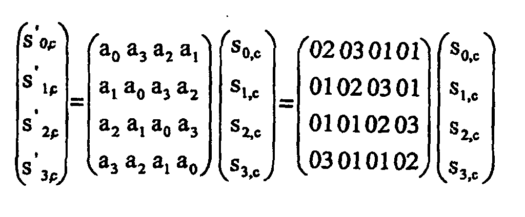
- the 128-bit blocks being processed are conveniently represented as 16 8-bit blocks in a 4 ⁇ 4 matrix, as s row, column , according to the pattern, s 0,0 s 0,1 s 0,2 s 0,3 s 1,0 s 1,1 s 1,2 s 1,3 s 2,0 s 2,1 s 2,2 s 2,3 s 3,0 s 3,1 s 3,2 s 3,3
- the polynomial is co-prime to x 4 + 1 and is therefore invertible.
- the MixColumns transform can therefore be expressed as s r,c ⁇ s' r,c , for each of the columns in s.
- each successive row is a shifted or rotated version of the preceding row.
- each element in a row appears in every row but in a different position in the row, and specifically, for the MixColumns transform matrix the different position of each element for each row constitutes a single position right shift or rotation.
- Figure 2 illustrates an exemplary embodiment of hardware logic 50 adapted for the multiplication of an m ⁇ n matrix by a 1 ⁇ n matrix, in which the relationship between each successive row of n elements of the m ⁇ n matrix is a predetermined row shift.
- the logic 50 comprises four 8-bit multiplication circuits 60 ... 63, four 8-bit XOR gates 70 ... 73 and four feedback / output registers 80 ... 83, shown as MixCol 0 ... MixCol 3 .
- Each multiplication circuit 70 ... 73 is adapted for multiplication of an input by one of the matrix coefficients c 0 , c 1 , c 2 , c 3 .
- Each of the XOR gates 70 ... 73 may be implemented using any appropriate combination of logic elements required to execute the appropriate logical combination of two inputs, as described hereinafter.
- each multiplication circuit 60 ... 63 is coupled to a first input of a corresponding XOR gate 70 ... 73.
- the output of each XOR gate 70 ... 73 is coupled to a corresponding MixCol register 80 ... 83.
- the output of each MixCol register 80 ... 83 is coupled to the second input of one of the XOR gates 70 ... 73 according to a feedback plan 90 ...
- the feedback plan 90 ... 93 implements the right row shift function between successive rows of the matrices a r,c (encryption) and b r,c (decryption) - more generally the matrix c r,c .
- s 0c , s 1c , s 2c , s 3c are sequentially offered to the multiplication logic 60 ... 63 on successive cycles.
- the registers MixCol 0 to MixCol 3 are pre-set to zero.
- the number of rows, m, in the matrix determines the number of cycles required, while the number of columns, n, determines the number of logic groups (multipliers 60 ... 63, XOR gates 70 ... 73, and registers 80 ... 83) required.
- the multiplication logic 60 ... 63 can be implemented using any suitable logic.
- the logic is provided for both encryption and decryption combining certain logic according to the following schedule.
- e 27 s 7 XNOR NAND(d, s 45 )
- e 26 s 6 XNOR NAND(d, s 347 )
- e 25 s 5 XNOR NAND(d, s 236 )
- e 24 s 4 XNOR NAND(d, s 125 )
- e 23 s 3 XNOR NAND(d, s 015 )
- e 22 s 2 XNOR NAND(d, s 0567 )
- e 21 s 1 XNOR NAND(d, s 67 )
- e 20 s 0 XNOR NAND(D, s 56 )
Landscapes
- Engineering & Computer Science (AREA)
- Physics & Mathematics (AREA)
- General Physics & Mathematics (AREA)
- Mathematical Optimization (AREA)
- Theoretical Computer Science (AREA)
- Pure & Applied Mathematics (AREA)
- Computational Mathematics (AREA)
- Mathematical Analysis (AREA)
- Computing Systems (AREA)
- Signal Processing (AREA)
- Computer Networks & Wireless Communication (AREA)
- Mathematical Physics (AREA)
- General Engineering & Computer Science (AREA)
- Computer Security & Cryptography (AREA)
- Complex Calculations (AREA)
- Organic Low-Molecular-Weight Compounds And Preparation Thereof (AREA)
- Saccharide Compounds (AREA)
- Compression, Expansion, Code Conversion, And Decoders (AREA)
- Pharmaceuticals Containing Other Organic And Inorganic Compounds (AREA)
- Storage Device Security (AREA)
- Curing Cements, Concrete, And Artificial Stone (AREA)
Abstract
Description
| s0,0 | s0,1 | s0,2 | s0,3 |
| s1,0 | s1,1 | s1,2 | s1,3 |
| s2,0 | s2,1 | s2,2 | s2,3 |
| s3,0 | s3,1 | s3,2 | s3,3 |
sr,c → s'r,c, for each of the columns in s.

Claims (15)
- A logic circuit for multiplication of an (m × n) matrix by a (1 × n) or by a (m × 1) matrix, where m is a number of rows and n is a number of columns, and wherein each successive row m of n elements is a predetermined row permutation of a preceding row, the circuit characterised in comprising:n multiplication circuits (60...63) each having an input and an output which returns the value of said input multiplied by a predetermined multiplicand;n logic circuits, (70...73) each for executing a predetermined logical combination of a first input and a second input to provide a logical output, the first input being coupled to the output of a corresponding one of the n multiplication circuits;n registers (80...83) for receiving said logical output;feedback logic for routing the contents of each register to a selected one of the second inputs in accordance with a feedback plan that corresponds to the predetermined row permutation; andcontrol means for successively providing as input to each of the n multiplication circuits each element in the (1 × n) or (m × 1) matrix.
- The logic circuit of claim 1 in which the feedback logic provides a feedback plan corresponding to said predetermined row permutation that is a row shift.
- The logic circuit of claim 2 in which the row shift is a single element right shift.
- The logic circuit of claim 1 in which the n logic circuits are each adapted to execute an XOR-combination of said first input and said second input.
- The logic circuit of claim 1 in which each of the predetermined multiplicands corresponds to one of the elements in the AES Rijndael MixColumns transform function.
- The logic circuit of claim 5 in which the number m = 4, the number n = 4, the multiplicand for the first multiplication circuit = 02, the multiplicand for the second multiplication circuit = 03, the multiplicand for the third multiplication circuit = 01, and the multiplicand for the fourth multiplication circuit = 01.
- The logic circuit of claim 5 in which the number m = 4, the number n = 4, the multiplicand for the first multiplication circuit = 0E, the multiplicand for the second multiplication circuit = 0B, the multiplicand for the third multiplication circuit = 0D, and the multiplicand for the fourth multiplication circuit = 09.
- The logic circuit of claim 6 or claim 7 in which the four multiplicands are switchable between the values in claim 6 and the values in claim 7.
- The logic circuit of claim 1 in which the control means is adapted to successively provide as input to each of the n multiplication circuits each successive element in the (1 × n) or (m × 1) matrix over each of n or m cycles of operation respectively.
- The logic circuit of claim 1 in which each of the n multiplication circuits, each of the n logic circuits, and each of the n registers are at least eight bits wide.
- The logic circuit of claim 1 in which the control means further includes means for providing as output from said logic circuit the contents of the n registers after each nth cycle.
- The logic circuit of claim 1 in which the control means further includes means for resetting each of the registers prior to the first calculation cycle.
- The logic circuit of claim 1 in which each successive row m of n elements is a predetermined row permutation of the immediately preceding row.
- An AES MixColumns transform circuit incorporating the logic circuit of any one of claims 1 to 13.
- An AES encryption and/or decryption engine incorporating the logic circuit of any one of claims 1 to 13 for performing the MixColumns transform.
Applications Claiming Priority (3)
| Application Number | Priority Date | Filing Date | Title |
|---|---|---|---|
| GBGB0213242.1A GB0213242D0 (en) | 2002-06-07 | 2002-06-07 | AES MixColumn transform |
| GB0213242 | 2002-06-07 | ||
| PCT/IB2003/002583 WO2003104973A1 (en) | 2002-06-07 | 2003-06-04 | Aes mixcolumn transform |
Publications (2)
| Publication Number | Publication Date |
|---|---|
| EP1514174A1 EP1514174A1 (en) | 2005-03-16 |
| EP1514174B1 true EP1514174B1 (en) | 2005-11-09 |
Family
ID=9938259
Family Applications (1)
| Application Number | Title | Priority Date | Filing Date |
|---|---|---|---|
| EP03732892A Expired - Lifetime EP1514174B1 (en) | 2002-06-07 | 2003-06-04 | Aes mixcolumn transform |
Country Status (9)
| Country | Link |
|---|---|
| US (1) | US7464130B2 (en) |
| EP (1) | EP1514174B1 (en) |
| JP (1) | JP2005529365A (en) |
| CN (1) | CN100541419C (en) |
| AT (1) | ATE309570T1 (en) |
| AU (1) | AU2003239700A1 (en) |
| DE (1) | DE60302249T2 (en) |
| GB (1) | GB0213242D0 (en) |
| WO (1) | WO2003104973A1 (en) |
Cited By (1)
| Publication number | Priority date | Publication date | Assignee | Title |
|---|---|---|---|---|
| US10601582B2 (en) | 2015-07-31 | 2020-03-24 | Joint Stock Company “InfoTeCS” | Method of linear transformation (variants) |
Families Citing this family (2)
| Publication number | Priority date | Publication date | Assignee | Title |
|---|---|---|---|---|
| KR100788902B1 (en) | 2006-12-06 | 2007-12-27 | 한국전자통신연구원 | Mixcolum block device and method of multiplication calculation thereof |
| CN103228593B (en) * | 2010-10-12 | 2015-07-29 | 奥林巴斯株式会社 | Photoconductive fiber glass |
Family Cites Families (3)
| Publication number | Priority date | Publication date | Assignee | Title |
|---|---|---|---|---|
| JPH06149862A (en) * | 1992-11-13 | 1994-05-31 | Sony Corp | Matrix data multiplying method and device |
| US6718465B1 (en) * | 2000-02-25 | 2004-04-06 | The Research Foundation Of State University Of New York | Reconfigurable inner product processor architecture implementing square recursive decomposition of partial product matrices |
| US7209939B2 (en) * | 2002-07-11 | 2007-04-24 | Sun Microsystems, Inc. | Precision improvement method for the Strassen/Winograd matrix multiplication method |
-
2002
- 2002-06-07 GB GBGB0213242.1A patent/GB0213242D0/en not_active Ceased
-
2003
- 2003-06-04 CN CN03813105.6A patent/CN100541419C/en not_active Expired - Lifetime
- 2003-06-04 DE DE60302249T patent/DE60302249T2/en not_active Expired - Lifetime
- 2003-06-04 AT AT03732892T patent/ATE309570T1/en not_active IP Right Cessation
- 2003-06-04 WO PCT/IB2003/002583 patent/WO2003104973A1/en active IP Right Grant
- 2003-06-04 JP JP2004511977A patent/JP2005529365A/en not_active Withdrawn
- 2003-06-04 AU AU2003239700A patent/AU2003239700A1/en not_active Abandoned
- 2003-06-04 EP EP03732892A patent/EP1514174B1/en not_active Expired - Lifetime
- 2003-06-04 US US10/516,846 patent/US7464130B2/en active Active
Cited By (1)
| Publication number | Priority date | Publication date | Assignee | Title |
|---|---|---|---|---|
| US10601582B2 (en) | 2015-07-31 | 2020-03-24 | Joint Stock Company “InfoTeCS” | Method of linear transformation (variants) |
Also Published As
| Publication number | Publication date |
|---|---|
| AU2003239700A1 (en) | 2003-12-22 |
| GB0213242D0 (en) | 2002-07-17 |
| DE60302249T2 (en) | 2006-08-03 |
| US20050182812A1 (en) | 2005-08-18 |
| WO2003104973A1 (en) | 2003-12-18 |
| DE60302249D1 (en) | 2005-12-15 |
| US7464130B2 (en) | 2008-12-09 |
| ATE309570T1 (en) | 2005-11-15 |
| CN100541419C (en) | 2009-09-16 |
| CN1659512A (en) | 2005-08-24 |
| JP2005529365A (en) | 2005-09-29 |
| EP1514174A1 (en) | 2005-03-16 |
Similar Documents
| Publication | Publication Date | Title |
|---|---|---|
| McLoone et al. | High performance single-chip FPGA Rijndael algorithm implementations | |
| US8290148B2 (en) | Encryption processing apparatus, encryption processing method, and computer program | |
| EP1246389B1 (en) | Apparatus for selectably encrypting or decrypting data | |
| US8346839B2 (en) | Efficient advanced encryption standard (AES) datapath using hybrid rijndael S-box | |
| US9515820B2 (en) | Protection against side channels | |
| US20020041685A1 (en) | Data encryption apparatus | |
| EP1257082A2 (en) | A computer useable product for generating data encryption/decryption apparatus | |
| JP2002366029A (en) | Encipherment safe against dpa(differential power analysis) | |
| CA2486713A1 (en) | Advanced encryption standard (aes) hardware cryptographic engine | |
| US20050169463A1 (en) | Hardware cryptographic engine and hardware cryptographic method using an efficient S-BOX implementation | |
| US20240187212A1 (en) | Method & apparatus for an ultra low power vlsi implementation of the 128-bit aes algorithm using a novel approach to the shiftrow transformation | |
| EP1764762B1 (en) | Electronic element and data processing method | |
| EP1514174B1 (en) | Aes mixcolumn transform | |
| Labbé et al. | AES Implementation on FPGA: Time-Flexibility Tradeoff | |
| Bajaj et al. | AES algorithm for encryption | |
| Naidu et al. | Design of high throughput and area efficient advanced encryption system core | |
| El Makhloufi et al. | Novel Approach Implementation of AES Algorithm Based on Radiation-Tolerant FPGA for Secure Mission in Satellite Remote Sensing: LST-SW case | |
| EP1629626B1 (en) | Method and apparatus for a low memory hardware implementation of the key expansion function | |
| Zigiotto et al. | A low-cost FPGA implementation of the Advanced Encryption Standard algorithm | |
| Lai et al. | A novel memoryless AES cipher architecture for networking applications | |
| Shylashree et al. | FPGA implementations of advanced encryption standard: A survey | |
| Socha et al. | Dynamic logic reconfiguration based side-channel protection of aes and serpent | |
| EP2209252B1 (en) | Compact hardware implementation of block ciphers with a MISTY structure | |
| Lanjewar et al. | Implementation of AES-256 Bit: A Review | |
| Hossain et al. | Reconfigurable encryption system: Encrypt digital data |
Legal Events
| Date | Code | Title | Description |
|---|---|---|---|
| PUAI | Public reference made under article 153(3) epc to a published international application that has entered the european phase |
Free format text: ORIGINAL CODE: 0009012 |
|
| 17P | Request for examination filed |
Effective date: 20050107 |
|
| AK | Designated contracting states |
Kind code of ref document: A1 Designated state(s): AT BE BG CH CY CZ DE DK EE ES FI FR GB GR HU IE IT LI LU MC NL PT RO SE SI SK TR |
|
| AX | Request for extension of the european patent |
Extension state: AL LT LV MK |
|
| GRAP | Despatch of communication of intention to grant a patent |
Free format text: ORIGINAL CODE: EPIDOSNIGR1 |
|
| GRAS | Grant fee paid |
Free format text: ORIGINAL CODE: EPIDOSNIGR3 |
|
| GRAA | (expected) grant |
Free format text: ORIGINAL CODE: 0009210 |
|
| AK | Designated contracting states |
Kind code of ref document: B1 Designated state(s): AT BE BG CH CY CZ DE DK EE ES FI FR GB GR HU IE IT LI LU MC NL PT RO SE SI SK TR |
|
| PG25 | Lapsed in a contracting state [announced via postgrant information from national office to epo] |
Ref country code: AT Free format text: LAPSE BECAUSE OF FAILURE TO SUBMIT A TRANSLATION OF THE DESCRIPTION OR TO PAY THE FEE WITHIN THE PRESCRIBED TIME-LIMIT Effective date: 20051109 Ref country code: SK Free format text: LAPSE BECAUSE OF FAILURE TO SUBMIT A TRANSLATION OF THE DESCRIPTION OR TO PAY THE FEE WITHIN THE PRESCRIBED TIME-LIMIT Effective date: 20051109 Ref country code: SI Free format text: LAPSE BECAUSE OF FAILURE TO SUBMIT A TRANSLATION OF THE DESCRIPTION OR TO PAY THE FEE WITHIN THE PRESCRIBED TIME-LIMIT Effective date: 20051109 Ref country code: RO Free format text: LAPSE BECAUSE OF FAILURE TO SUBMIT A TRANSLATION OF THE DESCRIPTION OR TO PAY THE FEE WITHIN THE PRESCRIBED TIME-LIMIT Effective date: 20051109 Ref country code: NL Free format text: LAPSE BECAUSE OF FAILURE TO SUBMIT A TRANSLATION OF THE DESCRIPTION OR TO PAY THE FEE WITHIN THE PRESCRIBED TIME-LIMIT Effective date: 20051109 Ref country code: LI Free format text: LAPSE BECAUSE OF FAILURE TO SUBMIT A TRANSLATION OF THE DESCRIPTION OR TO PAY THE FEE WITHIN THE PRESCRIBED TIME-LIMIT Effective date: 20051109 Ref country code: FI Free format text: LAPSE BECAUSE OF FAILURE TO SUBMIT A TRANSLATION OF THE DESCRIPTION OR TO PAY THE FEE WITHIN THE PRESCRIBED TIME-LIMIT Effective date: 20051109 Ref country code: CZ Free format text: LAPSE BECAUSE OF FAILURE TO SUBMIT A TRANSLATION OF THE DESCRIPTION OR TO PAY THE FEE WITHIN THE PRESCRIBED TIME-LIMIT Effective date: 20051109 Ref country code: CH Free format text: LAPSE BECAUSE OF FAILURE TO SUBMIT A TRANSLATION OF THE DESCRIPTION OR TO PAY THE FEE WITHIN THE PRESCRIBED TIME-LIMIT Effective date: 20051109 Ref country code: BE Free format text: LAPSE BECAUSE OF FAILURE TO SUBMIT A TRANSLATION OF THE DESCRIPTION OR TO PAY THE FEE WITHIN THE PRESCRIBED TIME-LIMIT Effective date: 20051109 Ref country code: IT Free format text: LAPSE BECAUSE OF FAILURE TO SUBMIT A TRANSLATION OF THE DESCRIPTION OR TO PAY THE FEE WITHIN THE PRESCRIBED TIME-LIMIT;WARNING: LAPSES OF ITALIAN PATENTS WITH EFFECTIVE DATE BEFORE 2007 MAY HAVE OCCURRED AT ANY TIME BEFORE 2007. THE CORRECT EFFECTIVE DATE MAY BE DIFFERENT FROM THE ONE RECORDED. Effective date: 20051109 |
|
| REG | Reference to a national code |
Ref country code: GB Ref legal event code: FG4D |
|
| REG | Reference to a national code |
Ref country code: CH Ref legal event code: EP |
|
| REG | Reference to a national code |
Ref country code: IE Ref legal event code: FG4D |
|
| REF | Corresponds to: |
Ref document number: 60302249 Country of ref document: DE Date of ref document: 20051215 Kind code of ref document: P |
|
| PG25 | Lapsed in a contracting state [announced via postgrant information from national office to epo] |
Ref country code: SE Free format text: LAPSE BECAUSE OF FAILURE TO SUBMIT A TRANSLATION OF THE DESCRIPTION OR TO PAY THE FEE WITHIN THE PRESCRIBED TIME-LIMIT Effective date: 20060209 Ref country code: GR Free format text: LAPSE BECAUSE OF FAILURE TO SUBMIT A TRANSLATION OF THE DESCRIPTION OR TO PAY THE FEE WITHIN THE PRESCRIBED TIME-LIMIT Effective date: 20060209 Ref country code: DK Free format text: LAPSE BECAUSE OF FAILURE TO SUBMIT A TRANSLATION OF THE DESCRIPTION OR TO PAY THE FEE WITHIN THE PRESCRIBED TIME-LIMIT Effective date: 20060209 Ref country code: BG Free format text: LAPSE BECAUSE OF FAILURE TO SUBMIT A TRANSLATION OF THE DESCRIPTION OR TO PAY THE FEE WITHIN THE PRESCRIBED TIME-LIMIT Effective date: 20060209 |
|
| PG25 | Lapsed in a contracting state [announced via postgrant information from national office to epo] |
Ref country code: ES Free format text: LAPSE BECAUSE OF FAILURE TO SUBMIT A TRANSLATION OF THE DESCRIPTION OR TO PAY THE FEE WITHIN THE PRESCRIBED TIME-LIMIT Effective date: 20060220 |
|
| PG25 | Lapsed in a contracting state [announced via postgrant information from national office to epo] |
Ref country code: PT Free format text: LAPSE BECAUSE OF FAILURE TO SUBMIT A TRANSLATION OF THE DESCRIPTION OR TO PAY THE FEE WITHIN THE PRESCRIBED TIME-LIMIT Effective date: 20060410 |
|
| NLV1 | Nl: lapsed or annulled due to failure to fulfill the requirements of art. 29p and 29m of the patents act | ||
| PG25 | Lapsed in a contracting state [announced via postgrant information from national office to epo] |
Ref country code: HU Free format text: LAPSE BECAUSE OF FAILURE TO SUBMIT A TRANSLATION OF THE DESCRIPTION OR TO PAY THE FEE WITHIN THE PRESCRIBED TIME-LIMIT Effective date: 20060510 |
|
| REG | Reference to a national code |
Ref country code: CH Ref legal event code: PL |
|
| PG25 | Lapsed in a contracting state [announced via postgrant information from national office to epo] |
Ref country code: IE Free format text: LAPSE BECAUSE OF NON-PAYMENT OF DUE FEES Effective date: 20060605 |
|
| PG25 | Lapsed in a contracting state [announced via postgrant information from national office to epo] |
Ref country code: MC Free format text: LAPSE BECAUSE OF NON-PAYMENT OF DUE FEES Effective date: 20060630 |
|
| ET | Fr: translation filed | ||
| PLBE | No opposition filed within time limit |
Free format text: ORIGINAL CODE: 0009261 |
|
| STAA | Information on the status of an ep patent application or granted ep patent |
Free format text: STATUS: NO OPPOSITION FILED WITHIN TIME LIMIT |
|
| 26N | No opposition filed |
Effective date: 20060810 |
|
| REG | Reference to a national code |
Ref country code: GB Ref legal event code: 732E |
|
| REG | Reference to a national code |
Ref country code: IE Ref legal event code: MM4A |
|
| REG | Reference to a national code |
Ref country code: FR Ref legal event code: TP |
|
| PG25 | Lapsed in a contracting state [announced via postgrant information from national office to epo] |
Ref country code: EE Free format text: LAPSE BECAUSE OF FAILURE TO SUBMIT A TRANSLATION OF THE DESCRIPTION OR TO PAY THE FEE WITHIN THE PRESCRIBED TIME-LIMIT Effective date: 20051109 |
|
| PG25 | Lapsed in a contracting state [announced via postgrant information from national office to epo] |
Ref country code: TR Free format text: LAPSE BECAUSE OF FAILURE TO SUBMIT A TRANSLATION OF THE DESCRIPTION OR TO PAY THE FEE WITHIN THE PRESCRIBED TIME-LIMIT Effective date: 20051109 Ref country code: LU Free format text: LAPSE BECAUSE OF NON-PAYMENT OF DUE FEES Effective date: 20060604 |
|
| PG25 | Lapsed in a contracting state [announced via postgrant information from national office to epo] |
Ref country code: CY Free format text: LAPSE BECAUSE OF FAILURE TO SUBMIT A TRANSLATION OF THE DESCRIPTION OR TO PAY THE FEE WITHIN THE PRESCRIBED TIME-LIMIT Effective date: 20051109 |
|
| REG | Reference to a national code |
Ref country code: FR Ref legal event code: PLFP Year of fee payment: 14 |
|
| REG | Reference to a national code |
Ref country code: FR Ref legal event code: PLFP Year of fee payment: 15 |
|
| REG | Reference to a national code |
Ref country code: FR Ref legal event code: PLFP Year of fee payment: 16 |
|
| PGFP | Annual fee paid to national office [announced via postgrant information from national office to epo] |
Ref country code: GB Payment date: 20220519 Year of fee payment: 20 Ref country code: FR Payment date: 20220519 Year of fee payment: 20 Ref country code: DE Payment date: 20220518 Year of fee payment: 20 |
|
| REG | Reference to a national code |
Ref country code: DE Ref legal event code: R071 Ref document number: 60302249 Country of ref document: DE |
|
| REG | Reference to a national code |
Ref country code: GB Ref legal event code: PE20 Expiry date: 20230603 |
|
| P01 | Opt-out of the competence of the unified patent court (upc) registered |
Effective date: 20230725 |
|
| PG25 | Lapsed in a contracting state [announced via postgrant information from national office to epo] |
Ref country code: GB Free format text: LAPSE BECAUSE OF EXPIRATION OF PROTECTION Effective date: 20230603 |