EP1513249A1 - Verfahren zur Symmetrierung eines Gleichspannungskreises einer Umrichterschaltung zur Schaltung von drei Spannungsniveaus - Google Patents
Verfahren zur Symmetrierung eines Gleichspannungskreises einer Umrichterschaltung zur Schaltung von drei Spannungsniveaus Download PDFInfo
- Publication number
- EP1513249A1 EP1513249A1 EP03405653A EP03405653A EP1513249A1 EP 1513249 A1 EP1513249 A1 EP 1513249A1 EP 03405653 A EP03405653 A EP 03405653A EP 03405653 A EP03405653 A EP 03405653A EP 1513249 A1 EP1513249 A1 EP 1513249A1
- Authority
- EP
- European Patent Office
- Prior art keywords
- voltage
- threshold value
- circuit
- dcs1
- phase
- Prior art date
- Legal status (The legal status is an assumption and is not a legal conclusion. Google has not performed a legal analysis and makes no representation as to the accuracy of the status listed.)
- Granted
Links
Images


Classifications
-
- H—ELECTRICITY
- H02—GENERATION; CONVERSION OR DISTRIBUTION OF ELECTRIC POWER
- H02M—APPARATUS FOR CONVERSION BETWEEN AC AND AC, BETWEEN AC AND DC, OR BETWEEN DC AND DC, AND FOR USE WITH MAINS OR SIMILAR POWER SUPPLY SYSTEMS; CONVERSION OF DC OR AC INPUT POWER INTO SURGE OUTPUT POWER; CONTROL OR REGULATION THEREOF
- H02M7/00—Conversion of AC power input into DC power output; Conversion of DC power input into AC power output
- H02M7/42—Conversion of DC power input into AC power output without possibility of reversal
- H02M7/44—Conversion of DC power input into AC power output without possibility of reversal by static converters
- H02M7/48—Conversion of DC power input into AC power output without possibility of reversal by static converters using discharge tubes with control electrode or semiconductor devices with control electrode
- H02M7/483—Converters with outputs that each can have more than two voltages levels
- H02M7/4833—Capacitor voltage balancing
-
- H—ELECTRICITY
- H02—GENERATION; CONVERSION OR DISTRIBUTION OF ELECTRIC POWER
- H02M—APPARATUS FOR CONVERSION BETWEEN AC AND AC, BETWEEN AC AND DC, OR BETWEEN DC AND DC, AND FOR USE WITH MAINS OR SIMILAR POWER SUPPLY SYSTEMS; CONVERSION OF DC OR AC INPUT POWER INTO SURGE OUTPUT POWER; CONTROL OR REGULATION THEREOF
- H02M7/00—Conversion of AC power input into DC power output; Conversion of DC power input into AC power output
- H02M7/42—Conversion of DC power input into AC power output without possibility of reversal
- H02M7/44—Conversion of DC power input into AC power output without possibility of reversal by static converters
- H02M7/48—Conversion of DC power input into AC power output without possibility of reversal by static converters using discharge tubes with control electrode or semiconductor devices with control electrode
- H02M7/483—Converters with outputs that each can have more than two voltages levels
- H02M7/487—Neutral point clamped inverters
Definitions
- the invention relates to the field of power electronics. She starts from one Method for balancing a DC voltage circuit of a converter circuit for Circuit of three voltage levels according to the preamble of the independent claim.
- Today high power voltage converters are used in many applications.
- Such a Inverter usually switches three voltage levels, including a DC voltage circuit is provided by a first capacitor and by a series to the first Capacitor switched second capacitor is formed.
- the DC voltage circuit furthermore has a first main connection on the first condenser, on the second condenser a second main terminal and one connected through the two serially connected Capacitors formed on part.
- the converter comprises the circuit of three voltage levels power semiconductor switch, which interconnects in the usual way are.
- the aforementioned DC voltage difference value is set to a predefinable monitored when the first threshold value is exceeded, wherein when the first threshold value is exceeded, i.e. if the first DC voltage is greater than the second DC voltage, or at Falling below the first threshold, i. if the second DC voltage is greater than the first DC voltage, the three phases after one of the switching state combinations selected switching state combination with the first main terminal, with the second Main connection or to the partial connection.
- the selection of suitable Switching state combination takes place as a function of the preceding switching state combination, the flow direction of a phase current and the overshoot or undershoot the first threshold.
- the object of the invention is therefore a method for balancing a DC voltage circuit an inverter circuit to indicate three voltage levels, by which even at a high modulation, i. at a high degree of modulation, Inequalities in the amounts of DC voltages across capacitors of the DC voltage circuit can be easily compensated.
- each phase of the inverter circuit is powered by power semiconductor switches the converter circuit after each predetermined sequence of switching states within a predetermined period of time with the first main terminal, with the second Main connection or connected to the partial connection, wherein the switching states of the phases are predetermined to each other by switching state combinations.
- the DC voltage difference value is monitored for a predefinable first threshold value is, wherein when exceeding or falling below the first threshold, the phases according to one of the switching state combinations depending on the preceding Switching state combination, the flow direction of a phase current and the crossing or falling below the first threshold selected switching state combination with the first main connection, with the second main connection or with the partial connection get connected.
- the degree of modulation for each phase is continuously determined and monitored for a predefinable modulation level threshold.
- the degree of modulation is according to the invention by selecting a sequence the predetermined sequences for a selectable period reduced.
- the first DC voltage or the second DC voltage are very easily influenced such that inequalities in the amounts between the first and second DC voltage can be compensated and thus a balancing of the DC voltage circuit done in a very simple way.
- the reduction of the degree of modulation by means of a certain predetermined sequence of switching states for a particular selectable period of time also makes it possible with advantage, the desired symmetrization of DC circuit even with a high modulation of the converter circuit, i. to achieve at a high degree of modulation.
- FIG. 1 an embodiment of a three-phase converter circuit for switching three voltage levels is shown.
- the converter circuit according to FIG. 1 has a DC voltage circuit 1 which is formed by a first capacitor C 1 and by a second capacitor C 2 connected in series with the first capacitor C 1 .
- the DC voltage circuit 1 has at the first capacitor C 1 a first main terminal V + , at the second capacitor C 2 a second main terminal V - and a partial terminal NP formed by the two series-connected capacitors C 1 , C 2 .
- each switching group 5, 6 7 is formed by two series-connected power semiconductor switches. Furthermore, in each partial converter system 4, the first switching group 5 is connected to the first main terminal V + and the second switching group 6 is connected to the second main terminal V - . Furthermore, the first switching group 5 is connected in series with the second switching group 6, wherein the connection point of the first switching group 5 with the second switching group 6 forms a phase connection.
- the third switching group 7, which is designed as a terminal switching group, is connected to the first switching group 5, in particular to the connection point of the two series-connected power semiconductor switches of the first switching group 5.
- the third switching group 7 is connected to the second switching group 6, in particular to the connection point of the two series-connected power semiconductor switches of the second switching group 6.
- the third switching group 7, in particular the connection point of the two series-connected power semiconductor switches of the third switching group 7, is connected to the partial connection NP.
- the power semiconductor switches of the first and second switching groups 5, 6 are designed as controllable bidirectional power semiconductor switches, wherein the power semiconductor switches of the third switching group are designed as unidirectional non-controllable semiconductor switches.
- the power semiconductor switches of the third switching group are designed as controllable bidirectional power semiconductor switches.
- a DC voltage U DC1 applied to the first capacitor C 1 and a DC voltage U DC2 applied to the second capacitor C 2 now become a DC voltage difference value U NP educated.
- each phase u, w, v of the converter circuit is connected by the power semiconductor switches after a predetermined sequence PM of switching states within a predetermined period of time to the first main terminal V + , to the second main terminal V - or to the partial terminal NP, the switching states of Phases u, v, w are given to each other by switching state combinations SK.
- FIG. 1 As already mentioned, FIG. 1
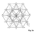
- FIG. 2 a shows a state diagram of these switching state combinations SK, where "+" for a connection of the corresponding phase u, v, w to the first main connection V + , "-" for a connection of the corresponding phase u, v, w with the second main connection V - and "0" for a connection of the corresponding phase u, v, w with the partial connection NP and the lines between the switching state combinations SK represent permissible transitions between the switching state combinations SK.
- FIG. 2 b shows typical time profiles of the phase voltages U u , U v , U w of the converter circuit according to FIG. 1.
- phase voltage U u , U v , U w are formed by the respective sequences PM of switching states, as an example in the phase voltage U u for the phase U a sequence PM for the first half of the period of the phase voltage U u is specially designated as the aforesaid predetermined period of time and a sequence PM for the second half of the period of the phase voltage U u is specified as the aforesaid predetermined time period.
- the phase voltages U v , U w of the phase v and phase w are shown in FIG. 2b from the phase voltage U u by a phase shift of 120 ° or 240 °. Such sequences are commonly referred to as so-called pulse patterns.
- the above-mentioned DC voltage difference value will continue to be used U NP monitored at a predetermined first threshold value U DCS1 out, wherein when exceeding or falling below the first threshold value U DCS1 the phases u, v, w after one of the switching state combinations SK depending on the preceding switching state combination SK, the flow direction of a phase current i u , i v , i w and the exceeding or falling below the first threshold value U DCS1 selected switching state combination SK with the first main terminal V + , with the second main terminal V - are connected to the sub-terminal NP or.
- the degree of modulation m for each phase is continuously determined and monitored for a predefinable modulation degree threshold value S m .
- the degree of modulation m is similar. If the first threshold value U DCS1 is exceeded or undershot and if the modulation degree threshold value S m is exceeded, the degree of modulation m is then reduced according to the invention by selecting a sequence PM from the predetermined sequences PM for a selectable period of time.
- the first DC voltage U DC1 and the second DC voltage U DC2 can be influenced very simply, since the reduction of the degree of modulation m from the first capacitor C 1 or from the second capacitor C 2 related energy is reduced. This is done in such a way that inequalities in the amounts between the first and second DC voltage U DC1 , U DC2 can be compensated and thus a balancing of the DC voltage circuit 1 can be achieved in a very simple manner.
- the reduction of the degree of modulation m by means of a specific predetermined sequence PM of switching states for a certain selectable period of time also makes it possible to achieve the desired balancing of the DC voltage circuit 1 even with a high modulation of the converter circuit, ie at a high degree of modulation m, in particular at m greater than 0, 8, to reach.
- the time course of the phase voltage U u and the associated degree of modulation is exemplified for the case in which the converter circuit is operated by a motor, ie that to the phases u, v, w electrical energy, for example, flows to an electrical load, and at the first threshold value U DCS1 is exceeded at any time, ie when the first DC voltage U DC1 is greater in magnitude than the second DC voltage U DC2 . It should be noted at this point that the time course of the phase voltage U u and the degree of modulation m according to FIG.
- the respective period mentioned above for the individual cases corresponds to the already mentioned first or second half of the period of the corresponding phase voltage U u , U v , U w .
- the first DC voltage U DC1 or the second DC voltage U DC2 case-specific, ie depending on the operating state of the converter circuit are very easily influenced in such a way that inequalities in the amounts between the first and second DC voltage U DC1 , U DC2 can be compensated and thus a balancing of the DC voltage circuit 1 can be achieved in a very simple manner.
- a sequence is selected to reduce the degree of modulation m, which the degree of modulation m in the order of 1% to 2% with respect to the actually too This degree of modulation provided m reduced.
- the phases u, v, w become one of the switching state combinations SK as a function of the preceding switching state combination SK, the flow direction of a Phase current i u , i v , i w and the exceeding or falling below the first threshold value U DCS1 selected switching state combination SK with the first main terminal V + , with the second main terminal V - or connected to the partial connection NP.
- the selected switching state combination SK only a number of phases u, v, w with the first main terminal V + and the remaining number of phases u, v, w with the sub-terminal NP or only a number of phases u, v, w with the second main terminal V - and the remaining part of the phases u, v, w is connected to the sub-terminal NP.
- a positive phase current i u of the phase u flows, ie the flow direction of the phase current i u is like in Fig. 1 for the corresponding phase u, for example, to an electrical load, directed, and is the first threshold U DCS1 exceeded, then is selected according to Fig. 2c as switching state combination SK 10.
- the first threshold value U DCS1 is preferably selected in the order of magnitude between 0 and 0.03, so that occurring inequalities in the amounts between the first and second DC voltage U DC1 , U DC2 by the aforementioned method steps when exceeding and falling below the first threshold value U DCS1 very early and thus can be compensated very quickly.
- the modulation degree threshold value S m is preferably selected in the order of 0.8, so that occurring inequalities in the amounts between the first and second DC voltage U DC1 , U DC2 by the above-mentioned method steps when exceeding and falling below the first threshold value U DCS1 and Exceeding the Modulationsgradschwellwerts S m very early and thus can be compensated very quickly.
- the DC differential value is used U NP also monitored for a predetermined second threshold value U DCS2 out.
- the second threshold value U DCS2 is greater in magnitude than the first threshold value U DCS1 .
- a first voltage reduction device 2 connected in parallel with the first capacitor C 1 is actuated according to FIG.
- a second voltage reduction device 3 connected in parallel with the second capacitor C 2 is actuated.
- the actuation of the first or second voltage reduction 2, 3, the degree of modulation can be carried out both at m under suitsenem Modulationsgradschwellwert S m is exceeded or already Modulationsgradschwellwert S m and the subsequent and above have already been explained in detail reduction.
- Decisive for the actuation of the first or second voltage reduction device 2, 3 is only exceeding or falling below the second threshold value U DCS2 .
- the first and second voltage reducing means 2, 3 are each formed by a resistor and a switch connected in series with the resistor, wherein the first and second voltage reducing means 2, 3 are actuated by closing the associated switch.
- the closure of the first switch takes place immediately when the second threshold value U DCS2 is exceeded and the closure of the second switch occurs immediately when the second threshold value U DCS2 is undershot .
- energy of the associated capacitor C 1 , C 2 is converted into heat in the associated resistor and thus the associated DC voltage U DC1 , U DC2 is reduced simply, quickly and effectively, so that the equalization of the two DC voltages U DC1 , U DC2 in desired mass.
- the actuation of the first and second voltage reduction means takes place in each case for a predetermined period of time. This period of time is preferably predetermined as a function of the thermal capacity of the resistor.
- the inventive method for balancing the DC circuit 1 of the converter circuit for switching three voltage levels is a very simple, efficient and therefore cost-effective solution, inequalities in the amounts of DC voltages U DC1 , U DC2 to the capacitors C 1 , C 2 of the DC circuit 1 to compensate for a high modulation of the converter circuit.
Landscapes
- Engineering & Computer Science (AREA)
- Power Engineering (AREA)
- Dc-Dc Converters (AREA)
- Inverter Devices (AREA)
Abstract
Description
- Fig. 1
- eine Ausführungsform einer dreiphasigen Umrichterschaltung zur Schaltung von drei Spannungsniveaus,
- Fig. 2a
- ein Zustandsdiagramm mit Schaltzustandkombinationen der Phasen der Umrichterschaltung,
- Fig. 2b
- typische Zeitverläufe der Phasenspannungen der Umrichterschaltung nach Fig. 1,
- Fig. 2c
- eine Tabelle mit aus Fig. 2a ausgewählten Schaltzustandskombinationen und
- Fig. 3
- ein Zeitverlauf einer Phasenspannung und zugehörigem Modulationsgrad.
- 1
- Gleichspannungskreis
- 2
- erste Spannungsreduziereinrichtung
- 3
- zweite Spannungsreduziereinrichtung
- 4
- Teilumrichtersystem
- 5
- erste Schaltgruppe
- 6
- zweite Schaltgruppe
- 7
- dritte Schaltgruppe
Claims (9)
- Verfahren zur Symmetrierung eines Gleichspannungskreises einer Umrichterschaltung zur Schaltung von drei Spannungsniveaus, bei dem der Gleichspannungskreis (1) durch einen ersten Kondensator (C1) und durch einen in Serie zum ersten Kondensator (C1) geschalteten zweiten Kondensator (C2) gebildet ist und am ersten Kondensator (C1) einen ersten Hauptanschluss (V+), am zweiten Kondensator (C2) einen zweiten Hauptanschluss (V-) und einen durch die zwei seriell verbundenen Kondensatoren (C1, C2) gebildeten Teilanschluss (NP) aufweist und aus einer am ersten Kondensator (C1) anliegenden ersten Gleichspannung (UDC1) und aus einer am zweiten Kondensator (C2) anliegenden zweiten Gleichspannung (UDC2) ein Gleichspannungsdifferenzwert (
UNP ) gebildet wird, wobei der Gleichspannungskreis (1),
bei dem jede Phase (u, v, w) der Umrichterschaltung durch Leistungshalbleiterschalter der Umrichterschaltung nach jeweils einer vorgegebenen Abfolge (PM) von Schaltzuständen innerhalb einer vorgegebenen Zeitdauer mit dem ersten Hauptanschluss (V+), mit dem zweiten Hauptanschluss (V-) oder mit dem Teilanschluss (NP) verbunden wird, wobei die Schaltzustände der Phasen (u, v, w) zueinander durch Schaltzustandskombinationen (SK) vorgegeben sind,
bei dem der Gleichspannungsdifferenzwert (UNP ) auf einen vorgebbaren ersten Schwellwert (UDCS1) hin überwacht wird, und
bei dem bei Überschreiten oder Unterschreiten des ersten Schwellwertes (UDCS1) die Phasen (u, v, w) nach einer aus den Schaltzustandskombinationen (SK) in Abhängigkeit der vorangehenden Schaltzustandskombination (SK), der Flussrichtung eines Phasenstromes (iu, iv, iw) und des Überschreitens oder des Unterschreitens des ersten Schwellwertes (UDCS1) ausgewählten Schaltzustandskombination (SK) mit dem ersten Hauptanschluss (V+), mit dem zweiten Hauptanschluss (V-) oder mit dem Teilanschluss (NP) verbunden werden, dadurch gekennzeichnet, dass der Modulationsgrad (m) für jede Phase (u, v, w) fortlaufend ermittelt wird und auf einen vorgebbaren Modulationsgradschwellwert (Sm) hin überwacht wird, und
dass bei Überschreiten oder Unterschreiten des ersten Schwellwertes (UDCS1) und bei Überschreiten des Modulationsgradschwellwertes (Sm) der Modulationsgrad (m) durch Auswahl einer Abfolge (PM) aus den vorgegebenen Abfolgen (PM) für einen wählbaren Zeitraum verringert wird. - Verfahren nach Anspruch 1, dadurch gekennzeichnet, dass als Zeitraum für die Verringerung des Modulationsgrades (m) einer jeden Phase (u, v, w) bei motorischem Betrieb der Umrichterschaltung und bei Überschreiten des ersten Schwellwertes (UDCS1) oder bei generatorischem Betrieb der Umrichterschaltung und bei Unterschreiten des ersten Schwellwertes (UDCS1) die negative Halbschwingung der zugehörigen Phasenspannungsgrundschwingung gewählt wird.
- Verfahren nach einem der Ansprüche 1 oder 2 dadurch gekennzeichnet, dass als Zeitraum für die Verringerung des Modulationsgrades (m) einer jeden Phase (u, v, w) bei generatorischem Betrieb der Umrichterschaltung und bei Überschreiten des ersten Schwellwertes (UDCS1) oder bei motorischem Betrieb der Umrichterschaltung und bei Unterschreiten des ersten Schwellwertes (UDCS1) die positive Halbschwingung der zugehörigen Phasenspannungsgrundschwingung gewählt wird.
- Verfahren einem der vorhergehenden Ansprüche, dadurch gekennzeichnet, dass bei der ausgewählten Schaltzustandskombination (SK) nur eine Anzahl der Phasen (u, v, w) mit dem ersten Hauptanschluss (V+) und die restliche Anzahl der Phasen (u, v, w) mit dem Teilanschluss (NP) oder nur eine Anzahl der Phasen (u, v, w) mit dem zweiten Hauptanschluss (V-) und der restliche Teil der Phasen (u, v, w) mit dem Teilanschluss (NP) verbunden wird.
- Verfahren nach einem der vorhergehenden Ansprüche, dadurch gekennzeichnet, dass der erste Schwellwert (UDCS1) in der Grössenordnung von zwischen 0 und 0.03 gewählt wird.
- Verfahren nach einem der vorhergehenden Ansprüche, dadurch gekennzeichnet, dass der Modulationsgradschwellwert (Sm) in der Grössenordnung von 0,8 gewählt wird.
- Verfahren nach einem der vorhergehenden Ansprüche, dadurch gekennzeichnet, dass der Gleichspannungsdifferenzwert (
UNP ) auf einen vorgebbaren zweiten Schwellwert (UDCS2) hin überwacht wird,
bei Überschreiten des ersten Schwellwertes (UDCS1) und bei Überschreiten des zweiten Schwellwertes (UDCS2) eine erste parallel zum ersten Kondensator (C1) geschaltete Spannungsreduziereinrichtung (2) betätigt wird, und
dass bei Unterschreiten des ersten Schwellwertes (UDCS1) und bei Unterschreiten des zweiten Schwellwertes (UDCS2) eine zweite parallel zum zweiten Kondensator (C2) geschaltete Spannungsreduziereinrichtung (3) betätigt wird. - Verfahren nach Anspruch 7, dadurch gekennzeichnet, dass die erste und zweite Spannungsreduziereinrichtung (2, 3) jeweils durch einen Widerstand und einen in Serie zum Widerstand geschalteten Schalter gebildet ist und die erste und zweite Spannungsreduziereinrichtung (2, 3) durch Schliessen des zugehörigen Schalters betätigt wird.
- Verfahren nach Anspruch 7 oder 8, dadurch gekennzeichnet, dass die Betätigung der ersten und zweiten Spannungsreduziereinrichtung (2, 3) jeweils für eine vorgegeben Zeitdauer erfolgt.
Priority Applications (3)
| Application Number | Priority Date | Filing Date | Title |
|---|---|---|---|
| DE50305641T DE50305641D1 (de) | 2003-09-08 | 2003-09-08 | Verfahren zur Symmetrierung eines Gleichspannungskreises einer Umrichterschaltung zur Schaltung von drei Spannungsniveaus |
| EP03405653A EP1513249B1 (de) | 2003-09-08 | 2003-09-08 | Verfahren zur Symmetrierung eines Gleichspannungskreises einer Umrichterschaltung zur Schaltung von drei Spannungsniveaus |
| AT03405653T ATE344983T1 (de) | 2003-09-08 | 2003-09-08 | Verfahren zur symmetrierung eines gleichspannungskreises einer umrichterschaltung zur schaltung von drei spannungsniveaus |
Applications Claiming Priority (1)
| Application Number | Priority Date | Filing Date | Title |
|---|---|---|---|
| EP03405653A EP1513249B1 (de) | 2003-09-08 | 2003-09-08 | Verfahren zur Symmetrierung eines Gleichspannungskreises einer Umrichterschaltung zur Schaltung von drei Spannungsniveaus |
Publications (2)
| Publication Number | Publication Date |
|---|---|
| EP1513249A1 true EP1513249A1 (de) | 2005-03-09 |
| EP1513249B1 EP1513249B1 (de) | 2006-11-08 |
Family
ID=34130409
Family Applications (1)
| Application Number | Title | Priority Date | Filing Date |
|---|---|---|---|
| EP03405653A Expired - Lifetime EP1513249B1 (de) | 2003-09-08 | 2003-09-08 | Verfahren zur Symmetrierung eines Gleichspannungskreises einer Umrichterschaltung zur Schaltung von drei Spannungsniveaus |
Country Status (3)
| Country | Link |
|---|---|
| EP (1) | EP1513249B1 (de) |
| AT (1) | ATE344983T1 (de) |
| DE (1) | DE50305641D1 (de) |
Cited By (8)
| Publication number | Priority date | Publication date | Assignee | Title |
|---|---|---|---|---|
| WO2007028298A1 (fr) * | 2005-09-09 | 2007-03-15 | Changan Zhang | Procede de commande numerique pour onduleurs et conversion de frequence |
| ITCZ20090007A1 (it) * | 2009-05-04 | 2010-11-05 | Univ Calabria | Metodo di conversione di energia elettrica continua in energia elettrica alternata |
| US7916995B2 (en) | 2005-04-15 | 2011-03-29 | Thomson Licensing | Method and device for recording digital data |
| EP2555411A1 (de) * | 2011-08-03 | 2013-02-06 | Ingeteam Technology S.A. | Leistungsumwandler |
| DE102011084473A1 (de) * | 2011-10-13 | 2013-04-18 | Continental Automotive Gmbh | Verfahren zum Symmetrieren von Speicherzellen einer Speichervorrichtung und Speichersystem zum Durchführen des Verfahrens |
| CN111181430A (zh) * | 2020-01-10 | 2020-05-19 | 山东大学 | 低电压穿越条件下三电平逆变器中点平衡控制方法及系统 |
| CN113179040A (zh) * | 2021-04-19 | 2021-07-27 | 安徽建筑大学 | 三相三电平逆变器中点电位平衡及共模电压的抑制方法 |
| WO2023066483A1 (en) * | 2021-10-21 | 2023-04-27 | Huawei Technologies Co., Ltd. | Power conversion system for reducing dc-link capacitor stress |
Families Citing this family (2)
| Publication number | Priority date | Publication date | Assignee | Title |
|---|---|---|---|---|
| US8441820B2 (en) * | 2010-09-29 | 2013-05-14 | General Electric Company | DC-link voltage balancing system and method for multilevel converters |
| CN105305863B (zh) * | 2015-10-10 | 2017-09-19 | 天津大学 | 一种三电平npc逆变器中点电位平衡控制方法 |
-
2003
- 2003-09-08 AT AT03405653T patent/ATE344983T1/de not_active IP Right Cessation
- 2003-09-08 EP EP03405653A patent/EP1513249B1/de not_active Expired - Lifetime
- 2003-09-08 DE DE50305641T patent/DE50305641D1/de not_active Expired - Lifetime
Non-Patent Citations (2)
| Title |
|---|
| ALONSO O ET AL: "Analysis of neutral-point voltage balancing problem in three-level neutral-point-clamped inverters with SVPWM modulation", IECON-2002. PROCEEDINGS OF THE 28TH. ANNUAL CONFERENCE OF THE IEEE INDUSTRIAL ELECTRONICS SOCIETY. SEVILLA, SPAIN, NOV. 5 - 8, 2002, ANNUAL CONFERENCE OF THE IEEE INDUSTRIAL ELECTRONICS SOCIETY, NEW YORK, NY: IEEE, US, vol. 1 OF 4. CONF. 28, 5 November 2002 (2002-11-05), pages 920 - 925, XP010632826, ISBN: 0-7803-7474-6 * |
| QIANG SONG ET AL: "A neutral-point potential balancing algorithm for three-level NPC inverters using analytically injected zero-sequence voltage", APEC 2003. 18TH. ANNUAL IEEE APPLIED POWER ELECTRONICS CONFERENCE AND EXPOSITION. MIAMI BEACH, FL, FEB. 9 - 13, 2003, ANNUAL APPLIED POWER ELECTRONICS CONFERENCE, NEW YORK, NY: IEEE, US, vol. 1 OF 2. CONF. 18, 9 February 2003 (2003-02-09), pages 228 - 233, XP010631516, ISBN: 0-7803-7768-0 * |
Cited By (10)
| Publication number | Priority date | Publication date | Assignee | Title |
|---|---|---|---|---|
| US7916995B2 (en) | 2005-04-15 | 2011-03-29 | Thomson Licensing | Method and device for recording digital data |
| WO2007028298A1 (fr) * | 2005-09-09 | 2007-03-15 | Changan Zhang | Procede de commande numerique pour onduleurs et conversion de frequence |
| ITCZ20090007A1 (it) * | 2009-05-04 | 2010-11-05 | Univ Calabria | Metodo di conversione di energia elettrica continua in energia elettrica alternata |
| EP2555411A1 (de) * | 2011-08-03 | 2013-02-06 | Ingeteam Technology S.A. | Leistungsumwandler |
| DE102011084473A1 (de) * | 2011-10-13 | 2013-04-18 | Continental Automotive Gmbh | Verfahren zum Symmetrieren von Speicherzellen einer Speichervorrichtung und Speichersystem zum Durchführen des Verfahrens |
| DE102011084473B4 (de) | 2011-10-13 | 2022-06-23 | Vitesco Technologies GmbH | Verfahren zum Symmetrieren von Speicherzellen einer Speichervorrichtung und Speichersystem zum Durchführen des Verfahrens |
| CN111181430A (zh) * | 2020-01-10 | 2020-05-19 | 山东大学 | 低电压穿越条件下三电平逆变器中点平衡控制方法及系统 |
| CN113179040A (zh) * | 2021-04-19 | 2021-07-27 | 安徽建筑大学 | 三相三电平逆变器中点电位平衡及共模电压的抑制方法 |
| CN113179040B (zh) * | 2021-04-19 | 2022-03-18 | 安徽建筑大学 | 三相三电平逆变器中点电位平衡及共模电压的抑制方法 |
| WO2023066483A1 (en) * | 2021-10-21 | 2023-04-27 | Huawei Technologies Co., Ltd. | Power conversion system for reducing dc-link capacitor stress |
Also Published As
| Publication number | Publication date |
|---|---|
| DE50305641D1 (de) | 2006-12-21 |
| ATE344983T1 (de) | 2006-11-15 |
| EP1513249B1 (de) | 2006-11-08 |
Similar Documents
| Publication | Publication Date | Title |
|---|---|---|
| EP2348627A1 (de) | Wandlerschaltung sowie Verfahren zum Betreiben einer mehrstufigen Wandlerschaltung | |
| EP1815586B1 (de) | Umrichterschaltung zur schaltung einer vielzahl von schaltspannungsniveaus | |
| EP1544992A1 (de) | Umrichterschaltung mit zwei Teilumrichtern | |
| EP2110939A1 (de) | Wechselrichter und Verfahren zum Steuern eines Wechselrichters mit fliegenden Kapazitäten | |
| EP2180586A1 (de) | Umrichterschaltung sowie Einheit und System mit einer solchen Umrichterschaltung | |
| EP1670135B1 (de) | Verfahren zum Betrieb einer rotierenden elektrischen Maschine | |
| EP1513249B1 (de) | Verfahren zur Symmetrierung eines Gleichspannungskreises einer Umrichterschaltung zur Schaltung von drei Spannungsniveaus | |
| EP3151405A1 (de) | Schaltung zur symmetrierung von kondensatorspannungen an kondensatoren in einem gleichspannungskreis | |
| EP1647089B1 (de) | Umrichterschaltung | |
| EP1870991A1 (de) | Verfahren zum Betrieb einer Umrichterschaltung | |
| EP2034606A1 (de) | Verfahren zum Betrieb einer rotierenden elektrischen Maschine | |
| EP3895312B1 (de) | Elektronischer schalter mit stromregulierung | |
| DE102009054785A1 (de) | Bremschopper | |
| EP1544994B1 (de) | Verbessertes Verfahren zur Symmetrierung eines Gleichspannungskreises einer Umrichterschaltung zur Schaltung von drei Spannungsniveaus | |
| EP3357152B1 (de) | Verfahren zum ansteuern eines multiphasigen synchronwandlers | |
| EP2966769A1 (de) | Betrieb eines modularen Multilevelstromrichters | |
| WO2004105225A2 (de) | Umrichterschaltung | |
| EP2409394B1 (de) | Verfahren zum betrieb einer umrichterschaltung sowie vorrichtung zur durchführung des verfahrens | |
| EP1298781B1 (de) | Stromrichterschaltungsanordnung sowie Verfahren zur Anpassung einer variablen Gleichspannung | |
| EP1198877B1 (de) | Elektrische schaltung, insbesondere für einen mittelspannungsstromrichter | |
| EP1479558A1 (de) | Traktionsumrichterschaltung zur Ankopplung an ein elektrisches Versorgungsnetz | |
| DE102021133245A1 (de) | Verfahren und Vorrichtung zum Kühlen eines oder mehrerer Leistungsbauelemente | |
| EP4254767A1 (de) | Verfahren und system zum modifizieren von trägersignalen bei einer phasenverschobenen pulsweitenmodulation | |
| DE102020003221A1 (de) | Verfahren zum Durchführen einer Pulsweitenmodulation in einem Wechselrichter | |
| EP4329180A1 (de) | Steuerverfahren für einen modularen bremssteller |
Legal Events
| Date | Code | Title | Description |
|---|---|---|---|
| PUAI | Public reference made under article 153(3) epc to a published international application that has entered the european phase |
Free format text: ORIGINAL CODE: 0009012 |
|
| AK | Designated contracting states |
Kind code of ref document: A1 Designated state(s): AT BE BG CH CY CZ DE DK EE ES FI FR GB GR HU IE IT LI LU MC NL PT RO SE SI SK TR |
|
| AX | Request for extension of the european patent |
Extension state: AL LT LV MK |
|
| 17P | Request for examination filed |
Effective date: 20050818 |
|
| AKX | Designation fees paid |
Designated state(s): AT BE BG CH CY CZ DE DK EE ES FI FR GB GR HU IE IT LI LU MC NL PT RO SE SI SK TR |
|
| GRAP | Despatch of communication of intention to grant a patent |
Free format text: ORIGINAL CODE: EPIDOSNIGR1 |
|
| GRAS | Grant fee paid |
Free format text: ORIGINAL CODE: EPIDOSNIGR3 |
|
| GRAA | (expected) grant |
Free format text: ORIGINAL CODE: 0009210 |
|
| AK | Designated contracting states |
Kind code of ref document: B1 Designated state(s): AT BE BG CH CY CZ DE DK EE ES FI FR GB GR HU IE IT LI LU MC NL PT RO SE SI SK TR |
|
| PG25 | Lapsed in a contracting state [announced via postgrant information from national office to epo] |
Ref country code: IT Free format text: LAPSE BECAUSE OF FAILURE TO SUBMIT A TRANSLATION OF THE DESCRIPTION OR TO PAY THE FEE WITHIN THE PRESCRIBED TIME-LIMIT;WARNING: LAPSES OF ITALIAN PATENTS WITH EFFECTIVE DATE BEFORE 2007 MAY HAVE OCCURRED AT ANY TIME BEFORE 2007. THE CORRECT EFFECTIVE DATE MAY BE DIFFERENT FROM THE ONE RECORDED. Effective date: 20061108 Ref country code: SK Free format text: LAPSE BECAUSE OF FAILURE TO SUBMIT A TRANSLATION OF THE DESCRIPTION OR TO PAY THE FEE WITHIN THE PRESCRIBED TIME-LIMIT Effective date: 20061108 Ref country code: RO Free format text: LAPSE BECAUSE OF FAILURE TO SUBMIT A TRANSLATION OF THE DESCRIPTION OR TO PAY THE FEE WITHIN THE PRESCRIBED TIME-LIMIT Effective date: 20061108 Ref country code: IE Free format text: LAPSE BECAUSE OF FAILURE TO SUBMIT A TRANSLATION OF THE DESCRIPTION OR TO PAY THE FEE WITHIN THE PRESCRIBED TIME-LIMIT Effective date: 20061108 Ref country code: CZ Free format text: LAPSE BECAUSE OF FAILURE TO SUBMIT A TRANSLATION OF THE DESCRIPTION OR TO PAY THE FEE WITHIN THE PRESCRIBED TIME-LIMIT Effective date: 20061108 Ref country code: SI Free format text: LAPSE BECAUSE OF FAILURE TO SUBMIT A TRANSLATION OF THE DESCRIPTION OR TO PAY THE FEE WITHIN THE PRESCRIBED TIME-LIMIT Effective date: 20061108 Ref country code: NL Free format text: LAPSE BECAUSE OF FAILURE TO SUBMIT A TRANSLATION OF THE DESCRIPTION OR TO PAY THE FEE WITHIN THE PRESCRIBED TIME-LIMIT Effective date: 20061108 Ref country code: FI Free format text: LAPSE BECAUSE OF FAILURE TO SUBMIT A TRANSLATION OF THE DESCRIPTION OR TO PAY THE FEE WITHIN THE PRESCRIBED TIME-LIMIT Effective date: 20061108 |
|
| REG | Reference to a national code |
Ref country code: GB Ref legal event code: FG4D Free format text: NOT ENGLISH |
|
| REG | Reference to a national code |
Ref country code: CH Ref legal event code: EP |
|
| REG | Reference to a national code |
Ref country code: IE Ref legal event code: FG4D Free format text: LANGUAGE OF EP DOCUMENT: GERMAN |
|
| REF | Corresponds to: |
Ref document number: 50305641 Country of ref document: DE Date of ref document: 20061221 Kind code of ref document: P |
|
| PG25 | Lapsed in a contracting state [announced via postgrant information from national office to epo] |
Ref country code: BG Free format text: LAPSE BECAUSE OF FAILURE TO SUBMIT A TRANSLATION OF THE DESCRIPTION OR TO PAY THE FEE WITHIN THE PRESCRIBED TIME-LIMIT Effective date: 20070208 Ref country code: SE Free format text: LAPSE BECAUSE OF FAILURE TO SUBMIT A TRANSLATION OF THE DESCRIPTION OR TO PAY THE FEE WITHIN THE PRESCRIBED TIME-LIMIT Effective date: 20070208 Ref country code: DK Free format text: LAPSE BECAUSE OF FAILURE TO SUBMIT A TRANSLATION OF THE DESCRIPTION OR TO PAY THE FEE WITHIN THE PRESCRIBED TIME-LIMIT Effective date: 20070208 |
|
| PG25 | Lapsed in a contracting state [announced via postgrant information from national office to epo] |
Ref country code: ES Free format text: LAPSE BECAUSE OF FAILURE TO SUBMIT A TRANSLATION OF THE DESCRIPTION OR TO PAY THE FEE WITHIN THE PRESCRIBED TIME-LIMIT Effective date: 20070219 |
|
| PG25 | Lapsed in a contracting state [announced via postgrant information from national office to epo] |
Ref country code: PT Free format text: LAPSE BECAUSE OF FAILURE TO SUBMIT A TRANSLATION OF THE DESCRIPTION OR TO PAY THE FEE WITHIN THE PRESCRIBED TIME-LIMIT Effective date: 20070409 |
|
| NLV1 | Nl: lapsed or annulled due to failure to fulfill the requirements of art. 29p and 29m of the patents act | ||
| ET | Fr: translation filed | ||
| GBV | Gb: ep patent (uk) treated as always having been void in accordance with gb section 77(7)/1977 [no translation filed] |
Effective date: 20061108 |
|
| REG | Reference to a national code |
Ref country code: IE Ref legal event code: FD4D |
|
| PLBE | No opposition filed within time limit |
Free format text: ORIGINAL CODE: 0009261 |
|
| STAA | Information on the status of an ep patent application or granted ep patent |
Free format text: STATUS: NO OPPOSITION FILED WITHIN TIME LIMIT |
|
| 26N | No opposition filed |
Effective date: 20070809 |
|
| PG25 | Lapsed in a contracting state [announced via postgrant information from national office to epo] |
Ref country code: GB Free format text: LAPSE BECAUSE OF FAILURE TO SUBMIT A TRANSLATION OF THE DESCRIPTION OR TO PAY THE FEE WITHIN THE PRESCRIBED TIME-LIMIT Effective date: 20061108 |
|
| BERE | Be: lapsed |
Owner name: ABB RESEARCH LTD. Effective date: 20070930 |
|
| PG25 | Lapsed in a contracting state [announced via postgrant information from national office to epo] |
Ref country code: GR Free format text: LAPSE BECAUSE OF FAILURE TO SUBMIT A TRANSLATION OF THE DESCRIPTION OR TO PAY THE FEE WITHIN THE PRESCRIBED TIME-LIMIT Effective date: 20070209 Ref country code: MC Free format text: LAPSE BECAUSE OF NON-PAYMENT OF DUE FEES Effective date: 20070930 |
|
| REG | Reference to a national code |
Ref country code: CH Ref legal event code: PL |
|
| PG25 | Lapsed in a contracting state [announced via postgrant information from national office to epo] |
Ref country code: CH Free format text: LAPSE BECAUSE OF NON-PAYMENT OF DUE FEES Effective date: 20070930 Ref country code: LI Free format text: LAPSE BECAUSE OF NON-PAYMENT OF DUE FEES Effective date: 20070930 |
|
| PG25 | Lapsed in a contracting state [announced via postgrant information from national office to epo] |
Ref country code: BE Free format text: LAPSE BECAUSE OF NON-PAYMENT OF DUE FEES Effective date: 20070930 |
|
| PG25 | Lapsed in a contracting state [announced via postgrant information from national office to epo] |
Ref country code: AT Free format text: LAPSE BECAUSE OF NON-PAYMENT OF DUE FEES Effective date: 20070908 |
|
| PG25 | Lapsed in a contracting state [announced via postgrant information from national office to epo] |
Ref country code: EE Free format text: LAPSE BECAUSE OF FAILURE TO SUBMIT A TRANSLATION OF THE DESCRIPTION OR TO PAY THE FEE WITHIN THE PRESCRIBED TIME-LIMIT Effective date: 20061108 |
|
| PG25 | Lapsed in a contracting state [announced via postgrant information from national office to epo] |
Ref country code: LU Free format text: LAPSE BECAUSE OF NON-PAYMENT OF DUE FEES Effective date: 20070908 Ref country code: CY Free format text: LAPSE BECAUSE OF FAILURE TO SUBMIT A TRANSLATION OF THE DESCRIPTION OR TO PAY THE FEE WITHIN THE PRESCRIBED TIME-LIMIT Effective date: 20061108 |
|
| PG25 | Lapsed in a contracting state [announced via postgrant information from national office to epo] |
Ref country code: HU Free format text: LAPSE BECAUSE OF FAILURE TO SUBMIT A TRANSLATION OF THE DESCRIPTION OR TO PAY THE FEE WITHIN THE PRESCRIBED TIME-LIMIT Effective date: 20070509 Ref country code: TR Free format text: LAPSE BECAUSE OF FAILURE TO SUBMIT A TRANSLATION OF THE DESCRIPTION OR TO PAY THE FEE WITHIN THE PRESCRIBED TIME-LIMIT Effective date: 20061108 |
|
| PGFP | Annual fee paid to national office [announced via postgrant information from national office to epo] |
Ref country code: DE Payment date: 20140922 Year of fee payment: 12 |
|
| PGFP | Annual fee paid to national office [announced via postgrant information from national office to epo] |
Ref country code: FR Payment date: 20140919 Year of fee payment: 12 |
|
| REG | Reference to a national code |
Ref country code: DE Ref legal event code: R119 Ref document number: 50305641 Country of ref document: DE |
|
| REG | Reference to a national code |
Ref country code: FR Ref legal event code: ST Effective date: 20160531 |
|
| PG25 | Lapsed in a contracting state [announced via postgrant information from national office to epo] |
Ref country code: DE Free format text: LAPSE BECAUSE OF NON-PAYMENT OF DUE FEES Effective date: 20160401 |
|
| PG25 | Lapsed in a contracting state [announced via postgrant information from national office to epo] |
Ref country code: FR Free format text: LAPSE BECAUSE OF NON-PAYMENT OF DUE FEES Effective date: 20150930 |